Other Parts Discussed in Thread: TPS65224-Q1, TPS65219, , TPS65224, AM62A7, AM62A3, AM62A7-Q1, AM62A3-Q1, USB2ANY, AM6442, TPS22918
Tool/software:
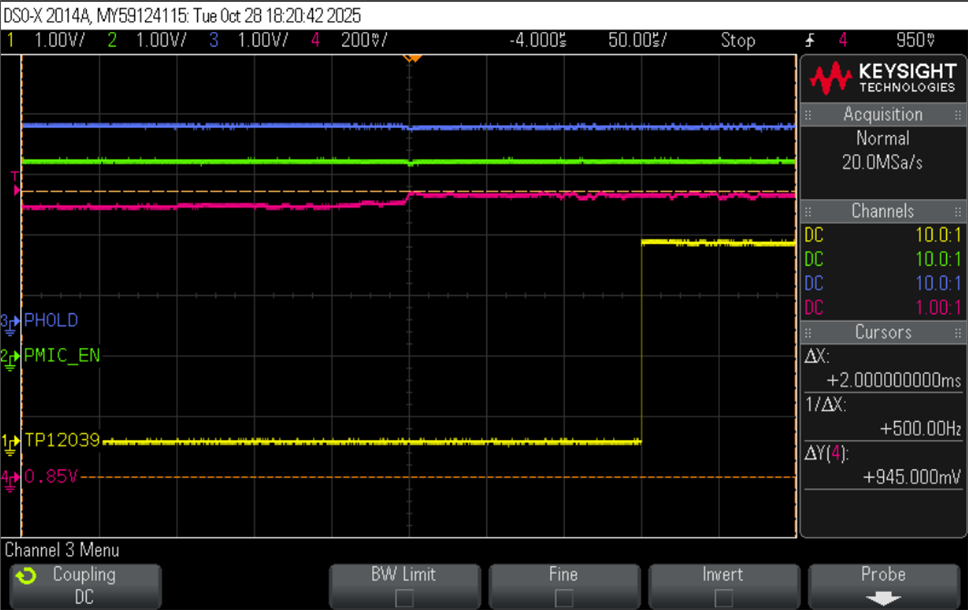
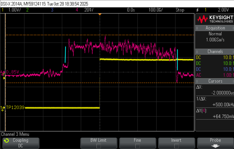
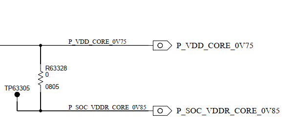
HI Board designers,
I am designing my board using TPS65224-Q1 PMIC
Are there some common recommendation or observations that i should be aware?