AM69: DQS to DQ Skew Issue with LPDDR4 write access

Part Number: AM69

Tool/software:

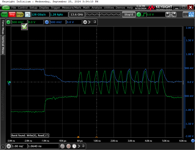
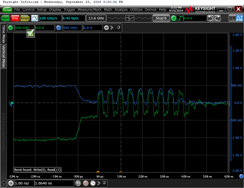
Our customer was performing compliance testing for LPDDR4 on their custom board and found an issue with write access. There is almost no skew between DQS and DQ, and DQS and DQ appear to be in phase. On the other hand, there are no issues with read access.

DQS to DQ Skew with write access:
DQS to DQ Skew with read access:
There are no issues with post-simulation in artwork, so there should be no issues with HW design.

Our customer is concerned that Write DQS2DQ Training did not work correctly.

Can the phase between DQS and DQ be manually adjusted? If so, how?

The syscfg file exported from the DDRSS Register Configuration Tool v0.11.0 is attached:

CUSTUM-AM69_LPDDR4.syscfg.txt
/**
 * These arguments were used when this file was generated. They will be automatically applied on subsequent loads
 * via the GUI or CLI. Run CLI with '--help' for additional information on how to override these arguments.
 * @cliArgs --device "J784S4_TDA4AP_TDA4VP_TDA4AH_TDA4VH_AM69x" --package "ALY" --part "Default" --product "TDA4x_DRA8x_AM67x-AM69x_DDR_Config@0.11.00.0000"
 * @versions {"tool":"1.20.0+3587"}
 */

/**
 * Import the modules used in this configuration.
 */
const DDRSS = scripting.addModule("/DDRSS");

/**
 * Write custom configuration values to the imported modules.
 */
DDRSS.system_cfg_msmc_intlv_size          = 8;
DDRSS.system_cfg_soc_number               = "AM69x";
DDRSS.lpddr4.$name                        = "jacinto_lpddr4_DDRSS_LPDDR40";
DDRSS.lpddr4.config_dram1_mr2_rl_FS2      = 36;
DDRSS.lpddr4.config_dram1_mr3_dbi_rd_FS2  = "Disable";
DDRSS.lpddr4.config_dram2_mr3_dbi_wr_FS2  = "Enable";
DDRSS.lpddr4.config_dram3_mr3_dbi_wr_FS2  = "Enable";
DDRSS.lpddr4.config_dram2_tREFIab_ns      = 1950;
DDRSS.lpddr4.config_dram2_tRASmax_ns      = 17550;
DDRSS.lpddr4.config_dram3_tREFIab_ns      = 1950;
DDRSS.lpddr4.config_dram3_tRASmax_ns      = 17550;
DDRSS.lpddr4.system_cfg_dram_density      = 8;
DDRSS.lpddr4.config_dram_tRFCab_ns        = 280;
DDRSS.lpddr4.config_dram_tRFCpb_ns        = 140;
DDRSS.lpddr4.config_dram_tXSR_ns          = 287.5;
DDRSS.lpddr4.config_dram_mr11_ca_odt_FS2  = "RZQ/5";
DDRSS.lpddr4.config_dram_mr11_dq_odt_FS2  = "RZQ/6";
DDRSS.lpddr4.system_cfg_dram1_density     = 8;
DDRSS.lpddr4.config_dram1_tRFCab_ns       = 280;
DDRSS.lpddr4.config_dram1_tRFCpb_ns       = 140;
DDRSS.lpddr4.config_dram1_tXSR_ns         = 287.5;
DDRSS.lpddr4.config_dram1_mr11_ca_odt_FS2 = "RZQ/5";
DDRSS.lpddr4.system_cfg_dram2_density     = 8;
DDRSS.lpddr4.config_dram2_tRFCab_ns       = 280;
DDRSS.lpddr4.config_dram2_tRFCpb_ns       = 140;
DDRSS.lpddr4.config_dram2_tXSR_ns         = 287.5;
DDRSS.lpddr4.config_dram2_mr11_ca_odt_FS2 = "RZQ/5";
DDRSS.lpddr4.system_cfg_dram3_density     = 8;
DDRSS.lpddr4.config_dram3_tRFCab_ns       = 280;
DDRSS.lpddr4.config_dram3_tRFCpb_ns       = 140;
DDRSS.lpddr4.config_dram3_tXSR_ns         = 287.5;
DDRSS.lpddr4.config_dram3_mr11_ca_odt_FS2 = "RZQ/5";
DDRSS.lpddr4.system_cfg_dram_ranks        = 1;
DDRSS.lpddr4.system_cfg_dram1_ranks       = 1;
DDRSS.lpddr4.system_cfg_dram2_ranks       = 1;
DDRSS.lpddr4.system_cfg_dram3_ranks       = 1;

Best regards,

Daisuke

  • Hello,

    Please expect a response next week due to the US Thanksgiving holidays. Most of our engineers are on vacation for the long weekend.

    Thanks.

  • Hi,

    There is almost no skew between DQS and DQ, and DQS and DQ appear to be in phase

    The LPDDR4 memory uses an un-matched DQS-DQ path (inside the memory); thus during a WRITE, the DQS strobe must arrive at the SDRAM ball prior to the DQ signal by the amount of tDQS2DQ. (which can range anywhere from 200 to 800 ps).

    The DQ is center aligned to the strobe only at the DRAM internal latch, which is not accessible with a scope / probe.

    Regards,
    Kevin

  • Hi Kevin-san,

    Thank you for your reply.

    The LPDDR4 memory uses an un-matched DQS-DQ path (inside the memory); thus during a WRITE, the DQS strobe must arrive at the SDRAM ball prior to the DQ signal by the amount of tDQS2DQ. (which can range anywhere from 200 to 800 ps).

    Does that mean the amount of tDQS2DQ is incorrect in the DDRSS Register Configuration Tool v0.11.0?

    If so, how can the amount of tDQS2DQ be set in the DDRSS Register Configuration Tool v0.11.0?

    Or does that mean the Write DQS2DQ Training did not work correctly?

    If so, why did the Write DQS2DQ Training not work correctly?

    Best regards,

    Daisuke

  • Hi Daisuke-san,

    Does that mean the amount of tDQS2DQ is incorrect in the DDRSS Register Configuration Tool v0.11.0?

    If so, how can the amount of tDQS2DQ be set in the DDRSS Register Configuration Tool v0.11.0?

    No - the timing relationship between DQS and DQ is set through write DQ training, which is performed during the initial boot as well as periodically during mission mode.

    Or does that mean the Write DQS2DQ Training did not work correctly?

    If so, why did the Write DQS2DQ Training not work correctly?

    No, it does not mean that training did not work correctly. The points I was trying to make are:

    1. You cannot probe what the internal latch of the memory observes (and it is at the internal latch where the DQ must be center-aligned to the strobe)
    2. Any WRITE measurement illustrating DQS vs. DQ on the PCB will have some delay offset between 200 to 800 ps which may give the illusion that the DQ and DQS "are in phase". 

    I do not know what data pattern is being transmitted on the bus during the provided waveform, but there seems to be a clear delay between DQS and DQ as the DQ signal is still switching during the DQS postamble phase.

  • Hi Kevin-san,

    Thank you for your reply.

    I understand that there is no abnormality in the waveform during write access attached.

    Our customer was performing compliance testing for LPDDR4 on their custom board and found an issue with write access.

    Could our customer be performing compliance testing incorrectly?

    For example, are inappropriate data patterns being used?

    Best regards,

    Daisuke

  • Hi Kevin-san,

    Could our customer be performing compliance testing incorrectly?

    For example, are inappropriate data patterns being used?

    Is it possible to perform compliance testing for write access?

    If so, how is compliance testing performed for write access?

    For tDQS2DQ measurement, at least in one burst, DQ should have a transition during the first bit; otherwise, the measured value may not be accurate.

    For DQ to transition during the first bit, should the data pattern be written as alternating 1b and 0b?

    I would appreciate it if you could give me some advice.

    Best regards,

    Daisuke

  • Hi Daisuke,

    Usually scope vendors offer compliance software that runs on the scope. There are different parameters which it may measure. Something like measuring the DQ eye size may be meaningful.  (example of compliance software: https://www.keysight.com/us/en/product/SW00DDRV/ddr-validation-license-suite.html ) 

    But if you are trying to compare the timing relationship between DQ and DQS during a WRITE, it needs to be understood that DQS and DQ are not skew matched inside the LPDDR4 memory, so one has to make assumptions as to what tDQS2DQ is, and that the controller appropriately accounts for it. 

    Regards,
    Kevin