Part Number: AM62A7
Other Parts Discussed in Thread: SYSCONFIG
Tool/software:
As mentioned, we’ve wired up our device per figure 2-1 of: AM62Ax/AM62Px LPDDR4 Board Design and Layout Guidelines
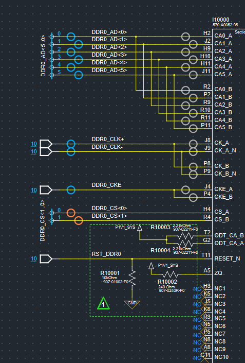
The memory device is dual die but with only one chip select per die, as CS_A and a CA_B.
Here’s the memory side of our schematic:

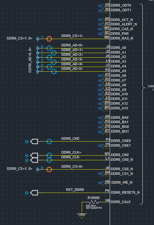
And here’s the processor side:

Essentially:
DDR0_CS0_N -> CS_A
DDR0_RAS_N -> CS_B
My concerns is that note [1] of that same figure indicates that the processor generates identical signals at these two pins, which seems incompatible with Nanya’s statement that “Our Datasheet is defined for separate signal for each x16 inside the package of NT6AN256T32AC-J2H”.
Our questions are:
- Is this the correct wiring configuration for this memory device?
- If so, what is the correct configuration nomenclature (e.g. dual-channel single-rank)?
- If not:
- What is the correct wiring configuration and nomenclature?
- What can we make work with what we have on these boards and how should it be configured?
We can do some rework of the PCB as necessary to get these into an operable state.


