Other Parts Discussed in Thread: TDA4VH-Q1, , TDA4AH-Q1, TDA4AP-Q1
Tool/software:
Hi all,
Looking at your datasheet "TDA4VH-Q1, TDA4AH-Q1, TDA4VP-Q1, TDA4AP-Q1 SPRSP79B – FEBRUARY 2023 – REVISED DECEMBER 2023", with respect to 200MHz HS400:
- Table 6-57:
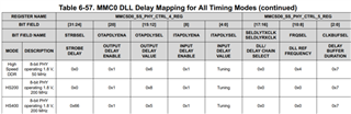
- Can I set the output delay (manually tune) with the mentioned registers? Or those values should be written and relate to the min/max values in the next tables?
If manual delay is optional –- what is the time resolution?
- Can you refer me to an elaborated guide regarding those registers settings
- Strobe delay is input, right? Is it delay relative to input data? If so, what is input delay?
- Can I set the output delay (manually tune) with the mentioned registers? Or those values should be written and relate to the min/max values in the next tables?
- Table 6-58:
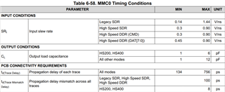
- Is there an SR input limitation for HS400/HS200?
- Is there a "valid window size" for HS400/200?
- What is the reason behind 8ps trace mismatch limitation? It's a lot tighter than other vendors we work with (50ps with another vendor)
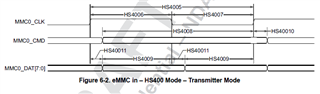
- Table 6-84:
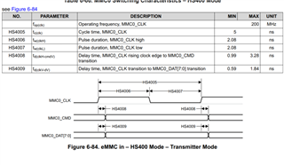
- As far as I know, HS400 is DDR. That doesn't agree with the timing diagram seen here or the numbers.
- Looking at HS4008, which is indeed SDR, like HS200 according to spec -
How can max delay be 3.28ns? UI is 2.5ns (nominal), and device samples at falling edge of clk, leaving negative (2.5-3.25ns) setup time
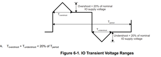
- Regarding Max/Min voltages for over/under shoots (transients) –
- Where can I find max/min allowed voltages for the input CMD/Data/Strobe? Is it under table 6.1?
If so, is it this section:
Or this one: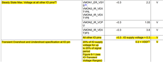
Is the 2.2V relative to PVT corner (i.e. 400mV above VDD) or is it 2.2V absolute, such that in PVT max I'll have 2.2-1.98=0.202V margin??
- Where can I find max/min allowed voltages for the input CMD/Data/Strobe? Is it under table 6.1?
Looking to hear from you,
- Yoel