


Tool/software:
Hi,
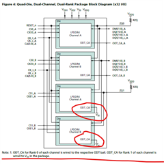
we use Micron: MT53E2G32D4DE-046 AAT:C, as you can see Rank1 ODT_CA connected to VSS, which means no address lines termination?
seems works on our prototype boards:
I noticed that:
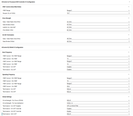
Termination - SOC ODT : RZQ/5
Termination - CA ODT: RZQ/3
Termination - DQ ODT: RZQ/6
Q1: why we have to set CA ODT not same as SOC ODT ?
I think we should set Both CA ODT and DQ ODT same as SOC ODT = RZQ/5 ==> 48 ohm.
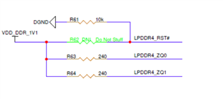
See our schematic:
Q2: can you provide value of MR11 and MR22 registers for each memory channel (A, B)?
Q3: SOC LPDDR4 driver is capable of 40 ohm / 60 ohm with 120 ohm pull-down?
Q4: Rank0 , CLK/CS/CA ODT termination enabled ?
Q5: Rank1, CLK/CS/CA ODT termination disabled ?
thanks
Max
