This thread has been locked.

If you have a related question, please click the "Ask a related question" button in the top right corner. The newly created question will be automatically linked to this question.

AM620-Q1: TI can support this GigaDevice QSPI NAND on AM620-Q1?

Part Number: AM620-Q1
Other Parts Discussed in Thread: SK-AM62-LP

Tool/software:

Dear TI expert.

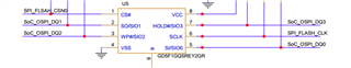
local customer wants to use GigaDevice QSPI FLASH, PN: GD5F1GQ5REY2GR, for their ADAS Application w/ AM620-Q1.

they choose Serial NAND boot mode, connect D0~D3 only as QSPI NAND has only 4 data lines.

and Using SK-AM62-LP EVM, hand work to solder GD5F1GQ5REY2GR  on board instead of W35N01JWTBAG.

they found that, at boot stage, the first command sent by AM6254 to read NAND parameter from address 01. But GigaDevice QSPI NAND need read from address 04. Then AM6254 can not read NAND parameters successfully, so subsequent data read error, Eventually it will not start.

would you please help check if if TI can support this GigaDevice QSPI NAND on AM620-Q1?

as they close to finish schematic design in this week, they wants us to help give quick response on the request ASAP

https://e2e.ti.com/cfs-file/__key/communityserver-discussions-components-files/791/serial_2D00_nand_2D00_1.8V.sal

DS-00845-GD5F1GQ5RExxG-Rev1.0_Automotive.pdf

Thanks a lot!

yong

  • Which of the following read commands did you meant to send?

  • Dear Kumar.

    I think it is 0x13.

    BTW, I sent the parse tool by email w/ TIDRIVER link, it can parse serial-nand-1.8V.sal and show the wave like above.

    thanks a lot!

    yong

  • Hi,

    I will check with the values which you have put forward. Will also confirm with the ROM team if required to get more inputs.

    I would also request to have all our conversation here rather over email to maintain consistency on our discussion.

    Thanks for your patience.

    Regards,

    Vaibhav

  • Dear Vaibhav.

    sure, we can get your support over E2E.

    I really want to ask your great support to highlight the request from customer and give quick response if go or not to go. then customer can move on.

    so may I ask if we can get response before 4/1/2025 IST?

    Thanks a lot!

    yong

  • Dear Vaibhav.

    soft reminder. 

    may I ask for the feedback?

    thanks a lot!

    yong

  • Hi Yong,

    31/03/2025 was a holiday here in TI Bangalore, India.

    I am actively looking at this query now.

    Regards,

    Vaibhav

  • Hi,

    Can you let me know the value of the following two fields?

    Regards,

    Vaibhav

  • Hello Yong,

    Any update on my question?

    I would need the values for bootmode pins 7 and 8 respectively.

    This way I can isolate which of the following is referenced.

    Looking forward to your response.

    Regards,

    Vaibhav

  • Dear Vaibhav.

    Yes, bit 7 and 8 are all 1.

    thanks a lot!

    yong

  • Hi Yong,

    Thanks for your patience.

    I appreciate you putting out this information.

    This means that you want the flash to start in 1S-1S-1S mode hence the following will be effective:

    On this note, for page reads 13h will be sent before the read command 0x0Bh is issued.

    Can you please check with the flash vendor about the following question?

    Q: Is the flash part GD5F1GQ5REY2GR set as BUF=1 or BUF=0? 

    More context, so ROM is set to work for BUF=1.

    BUF=1 is the Buffer Read Mode.

    BUF=0 is the Continuous Read Mode.


    Looking forward to your response.

    Regards,

    Vaibhav

  • Dear Vaibhav.

    please check below response from flash vendor:

    Q: Is the flash part GD5F1GQ5REY2GR set as BUF=1 or BUF=0? 

    • GD5F1GQ5REY2GR only supports buffer read mode but not continuous read mode, hence BUF=1.

    thanks a lot!

    yong

  • Hi Yong,

    Thanks for your response.

    GD5F1GQ5REY2GR only supports buffer read mode but not continuous read mode, hence BUF=1.

    This is ideal.

    So to summarize, you see that the flow is stuck at ROM and is not past ROM right?

    If that is the case, could you tell me if the following has been taken into consideration or not?

    If it is a YES, then I would redirect this thread to an expert who can review your schematics

    Looking forward to your response.

    Regards,

    Vaibhav

  • Dear Vaibhav.

    1. customer used SK-AM62-LP for the verification test, they remove W35N01JWTBAG and mount GD5F1GQ5REY2GR.

    2. HW connection like below as GD5F1GQ5REY2GR has only 4 data lines, D0~D3.

    CS# -> OSPI0_CSn0

    SO/SIO1     ->   OSPI0_D1

    WP#/SIO2   ->  OSPI0_D2

    VSS             -> Ground.

    VCC            -> 1.8V

    HOLD#/SIO3  -> OSPI0_D3

    SCLK           ->   OSPI0_CLK

    SI/SIO0        ->  OSPI0_D0

    3. they reports that the problem is that, "at boot stage, the first command sent by AM6254 to read NAND parameter from address 01. But GigaDevice QSPI NAND need read from address 04". they have asked GigaDevice to upgrade its NAND flash to address 01. then boot up is ok.

    Please let us know if the request is clear.

    thanks a lot!

    yong

  • Hi Yong,

    Thanks for your response.

    I have checked the Winbond flash datasheet and found out that the parameter page is at 0x1, I believe that is why 0x1 is read after 13h is issued.

    Please have a look at the following snippet:

    I have also seen and figured out that the GD flash part is a bit different as parameter page has page address of 0x4, and this is what ROM should be reading as well. I have found this from the datasheet, please see the relevant snippet:

    Allow me sometime to check if this can be modified at our end.

    Thanks for your patience.

    Regards,

    Vaibhav

  • Hi,

    I have checked and confirmed.

    Currently it is hardcoded/configured in ROM that the page address to read is 0x1, so currently it is not configurable.

    Hence, you would need to pick a flash part which has page address from 0x1, or the idea which you proposed as following, will also work.

    they have asked GigaDevice to upgrade its NAND flash to address 01. then boot up is ok.

    NOTE:

    Not my recommendation, but I found few GD flash parts which has page address at 0x1, like GD5F2GM7UE and GD5F2GM7RE.

    Marking the thread closed.

    Regards,

    Vaibhav