Tool/software:
There are some questions regarding the patch comments,
mmc: sdhci_am654: Add sdhci_am654_start_signal_voltage_switch
commit 93493662c0ad6878c8b01ed6d053ae99bc0bb76c upstream.
The sdhci_start_signal_voltage_switch function sets V1P8_SIGNAL_ENA by default after switching to 1v8 signaling. V1P8_SIGNAL_ENA determines whether to launch cmd/data on neg edge or pos edge of clock. Due to some eMMC and SD failures seen across am62x platform, do not set V1P8_SIGNAL_ENA by default, only enable the bit for devices that require this bit in order to switch to 1v8 voltage for uhs modes.
#1. Register HOST_CONTROL2 [V1P8_SIGNAL_ENA] bit description only mentioned control signal voltage. did not mention signal polarity. customer wants to know more details about how polarity related the voltage change? From which point change polarity from below #2 waveform
This bit controls voltage regulator for I/O cell. 3.3V is supplied to
the card regardless of signaling voltage. Setting this bit from 0 to
1 starts changing signal voltage from 3.3V to 1.8V. 1.8V regulator
output shall be stable within 5ms. Host Controller clears this bit if
switching to 1.8V signaling fails. Clearing this bit from 1 to 0 starts
changing signal voltage from 1.8V to 3.3V. 3.3V regulator output
shall be stable within 5ms. Host Driver can set this bit to 1 when
Host Controller supports 1.8V signaling [One of support bits is set to
1: SDR50, SDR104 or DDR50 in the Capabilities register] and the
card or device supports UHS-I. '0' 3.3V Signalling, '1' 1.8V Signalling
Reset Source: vbus_amod_g_rst_n 1 ENABLE 1.8V Signalling 0
DISABLE 3.3V Signalling
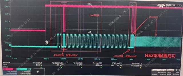
#2. Did not observe voltage change across eMMC initialization, cmd is always 3.3V, data is always 1.8V.
#3. “only enable the bit for devices that require this bit in order to switch to 1v8 voltage for UHS modes.”
How to know if the eMMC device need or not need set SDHCI_CTRL_VDD_180? there are seconds sources on customer side as eMMC is common device. will it cause incompatible。
And actually eMMC standard defined output in positive edge in single edge mode no matter what speed. What is the clock edge to output data/cmd before applying the patch? is it in negative edge?