 Hello Sir/Madam,
I am confused about the Pin VPxCTL0 and VPxCTL1 hookups of DM648 when the video port are configured as dual BT.656 SD inputs.
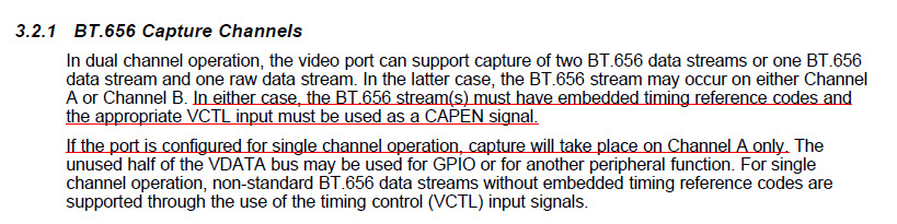
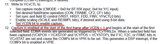
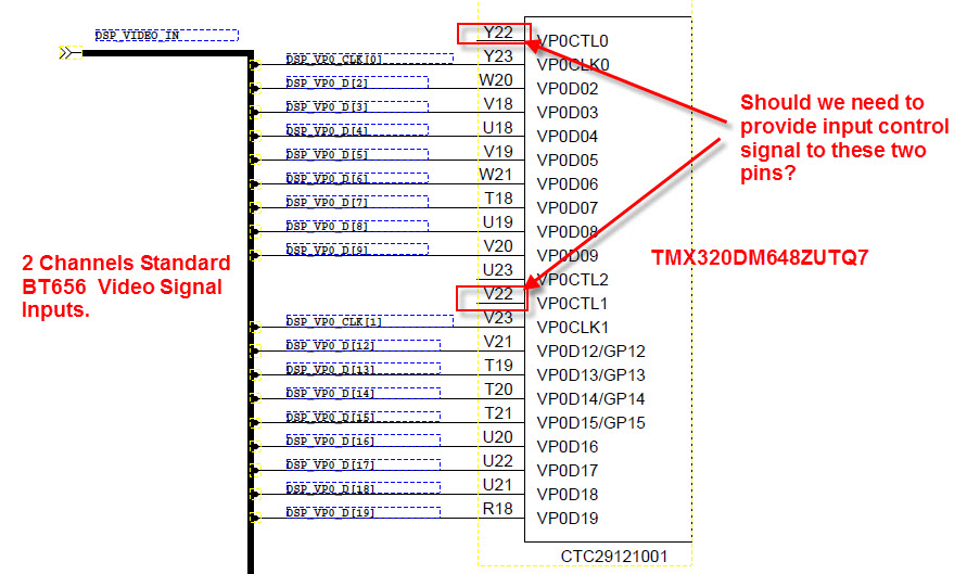
On page 48, Section 3.2.1 BT656 Capture Channels (TI document: spruem1b.pdf), it shows we have to provide a control signal input to VCTL to be functioned as CAPEN to enable the video capture. On page 28, Table 1-1 (TI document: spruem1b.pdf), it also shows we have to provide a control signal input to VPxCTL to be functioned as CAPEN. WHILE: On page 70-71, Capturing Video in BT656, Step 11-12, it shows only need SW to set the VCEN bit of register to enable capture. On page 71-72, Capturing Video in Raw Data Mode, Step 9-10, it shows need both HW (VPxCTL pin active) and SW to set the VCEN bit of register to enable capture. According the two items, it seems that when configuring dual channels BT.656 inputs, we do not need to use VPxCTL0 and VPxCTL1. Also, I did not find any connections for these pins when the video port is configured as dual BT.656 input channels in TI demo board schematic. Please help to clarify it.