This thread has been locked.

If you have a related question, please click the "Ask a related question" button in the top right corner. The newly created question will be automatically linked to this question.

TDA4VH-Q1: TPS6594133&tda4vh board

Part Number: TDA4VH-Q1

Tool/software:

Dear expert: 

     accroding to  Alert J784S4 E5 J742S2 E2 EVM Sys Updates v1.0.pdf

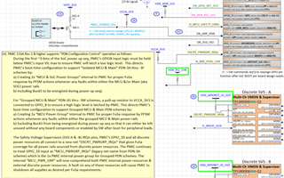
    GPIO 8 is EN_GRP_PDN type,  it will latch before 3ms step of power up seruence.  

     I want to know the 3ms from what time to what time ?

    When i connect it to Vsys_mcuio_3v3 , it seems latch 0 (I test the buck 5's output)

    when i connect it to  vsys_io_3v3 , it seems latch 1 I test the buck 5's output);

  I  am  confused with the result;

  • Latching of GPIO8 is 3ms from the assertion of EN_3V3_VIO control signal (sourced from GPIO9).  This is the 1st signal asserted by PMIC state machine starting execution of an SoC power up sequence.

    GPIO8 should be pulled up to VSYS_3V3 or VCCA_3V3 power rail since these supplies will be stable and are not included in the SoC power up sequence. Please see the snap-shot below taken from "PDN-3G scheme" (Grouped MCU & Main PDN type) that is part of the detailed "J784S4 EVM Single Leo Dual HCPS PDN-3AFGM v0.31" diagram (shown below).

    J784S4 EVM Single Leo Dual HCPS PDN-3AFGM v0.31.pdf

  • concerned :

    I am using PDN-3F ,  the GPIO-8 pin should be connected to where? 

    At proc141E4 : it pulled up to VSYS_MCUIO_3V3 NVM 2  

    AT PROC141E5: it pulled up to VCCA_3V3, but it contrloled by VDA_DLL_0V8    on PROC141E5  page 31 

    I think i will use buck 5 to power VDD_MCU_0V85, and   the GPIO8 should be latched 0 , is that right? 

    additonal question : 

    for my experiment:  3ms start with EN_VIO_3V3 , the VSYS_MCUIO_3V3‘s output is also firtst power, it shuoled latech 1 before 3 3ms, but it latch 0, seems wired?