This thread has been locked.

If you have a related question, please click the "Ask a related question" button in the top right corner. The newly created question will be automatically linked to this question.

DRA821U: GPIO output value change/MCSPI config performance

Expert 3730 points
Part Number: DRA821U

Tool/software:

Hi team,

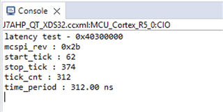
Customer is seeing that writing device registers such as GPIO output value change or configuring MCSPI takes quite a long time, almost 1us. This seems pretty low performance for such a powerful chip.

Couple questions on this:

- What might they be doing wrong that is causing this behavior?

- Is it a correct solution to increase the CBASS clock?

    • They tried to do this in u-boot using the procedure described in paragraph 5.4.5.7.4 (DRA821U TRM rev. D), but writing to PLLDIV1 and PLLDIV2 registers has no effect. They remain with values 24 (0x8017) and 1 (0x8000).
    • They are able to change the value of a PLL0_FREQ_CTRL0 register, but it influences too many other things.

Any advice on how to improve performance is appreciated!

Best,

Luke

  • Hi team, 

    Any update on this one?

    -Luke

  • Luke, 

    Which core did try to access which McSPI in that measurement? 

    Do you know how they did measure the latency? If the measurement had been done only one access, then the overhead of accessing PMU register (if they are using PMU) is not negligible and the code optimization would matter as well. 

    I don't currently have access any J7200 EVM. So, I tried to measure the SPI access in J784S2; Read MCSPI_REVISION register of MCU_MCSPI0_CFG from MCU R5f. Its read latency is 312ns. This value also includes some overhead of PMU register access and code optimization. I think that the actual access latency is less than this. 

    I expect the MCU domain structure should be not much different between J7200 vs J784S2.

    --Junbok 

  • Hi Junbok,

    They measured the latencies using oscilloscope and some other tools like VxWorks system viewer.

    I have to stress that they don’t have a problem with SPI, it works OK. They have a problem with an overhead. Accessing control and status registers take a lot of time. For example, the whole process including CS ON and CS off takes about 8-9 us while the SPI transfer takes only 2.5 us (32-bit transfer 12.5Mhz)

    The have same problem with GPIOs. For example they have a JAM player code from Intel that used JTAG protocol. The player controls GPIO pins that connected to the JTAG clock and data lines. When they used this code on the older chip the process took almost as twice less time.

    Best,

    Luke

  • Hi team,

    I understand there are likely many requests but could we get some feedback on what may be causing the above functionality? 
    - Luke

  • Luke, 

    I will ask SPI experts some help on analyzing SPI initialization latency.

  • Junbok,

    Thank you but the real concern here is the amount of time to toggle a GPIO pin. They have modified the GPIO driver to only access the GPIO pin if the state changes. This masks the problem somewhat but really doesn’t help.

    Best,

    Luke

  • Hello,

    What CPU-CORE and software are you using to control the GPIO?   Is this something like Linux or FreeRTOS or other?  It seems mostly likely that a software stack is in use which probably adds overhead and/or the CPU which is being used might not be clocked fully.  All of the cores do provide a hardware trace feature which jtag tools can make use of. A simple "step-over" the GPIO toggle C/C++ function can result in a complete trace of all the instructions executed and their time to completion.   In the case you describe I suspect you will see a lot of unexpected instructions executing due to SW overhead. 

    In the case of read-writing the GPIO, Junbok mentions the round trip time (launch-request, data, response) 'touch' to an IO space took ~300nS.  If your code is doing multiple accesses to the uncached IO address, an accumulation of instructions to a time of 1uS doesn't seem hard to believe.  A 'heavy' gpio library might read the block to make sure its enabled, then read/write to set the GPIO direction, then read (to get current value, apply a mask) then write out a value.   An ETM trace of what 'exactly' happens will illuminate what is going on. If its an A72, the CPU might be able to retire many instructions @2GHz from a local cache, but if its going across the bus and talking with a IO block which might be running a 20MHz (or even resync to a 32KHz debounce) it will by design take much longer.

    The SW in use, the # of actual instructions and to "where" and the relative clock speeds (soruce <-> interconnect <-> module) all matter.

    Regards,
    Richard W.