[FAQ] AM625 / AM623 / AM620-Q1 / AM62Ax / AM62Px / AM62D-Q1 / AM62L / AM64x / AM243x Design Recommendations / Custom board hardware design - Queries related to RMII interface and RMII TI EPHY

Part Number: AM62A3AM62PAM62A7AM6412AM2431AM620-Q1AM62D-Q1AM62P-Q1AM625-Q1AM2432AM62LAM62A1-Q1AM62A7-Q1AM6441AM6442AM2434AM6411AM625AM62A3-Q1AM6422AM623AM625SIP
Other Parts Discussed in Thread: AM62P, OMAP-L138, AM6442, DP83825I, AM623

Tool/software:

Hi TI experts,

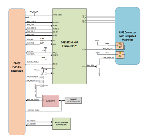
Please provide  guidelines for using RMII interface

Recommendations while using TI EPHY for RMII interface 

  • Hi Board designers,

    Refer below inputs regarding crystal 

    Information related to Crystal

    https://e2e.ti.com/support/processors-group/processors/f/processors-forum/1467149/am625-q1-crystal-accuracy/5629628

    Operating the PHY with a clock that has 100 PPM accuracy would violate the industry standard. Therefore, this is not supported. We only support a reference clock that has 50 PPM accuracy. The 50 PPM limit must include the initial accuracy of the clock source as well as the temperature variation and aging.

    Query relate to allowed SOC clock frequency

    The only crystal frequency supported is 25 MHz and the maximum deviation from that frequency being +/- 50 Parts Per Million (PPM) when using RMII or RGMII Ethernet peripherals. This limit is defined in the datasheet and means the frequency can only vary +/- 1250 Hz from the nominal frequency of 25 MHz for this use case. The limit doubles when not using RMII or RGMII.

    The device datasheet is correct. I do not know the purpose of the TISCI User Guide. I will need to discuss this with the software team. 

    It is very unlikely that something inside the device is causing the issue. Radiated emissions are most likely being generated by one or more of the peripherals signals. The customer needs to determine which peripheral is radiating emissions and look at their PCB layout and connectivity to the attached peripheral device to better understand why they have this issue. These type issues are typically caused when signals are not impedance controlled along its entire path. Radiation occurs when the electric fields generated by the fast signal transitions are allowed to radiate away from the signal where there are impedance discontinuities in the signal path.

    Power supply resonances can also radiate emissions, so they should check for noise on their power supplies.  


    FYI: The TRM content you referenced above has a note saying "Reference clock selections may be limited by the device. Please consult the device specific datasheet to determine which system clock frequencies are valid."

     The SoC has been qualified using a 25MHz Xtal only and TI will not qualify any other frequencies

    AM62P guidelines for using a crystal

    The spec shows that a crystal with 50ppm or less can be used for Ethernet.  TI’s EVM uses an oscillator instead.  Is there a special guideline for using a crystal?  Panasonic is concerned about the characteristics such as jitter when generating clocks from PLL using a crystal.

     The 50 PPM reference clock frequency accuracy requirement represents a limit defined in the RMII specification. Frequency error expressed in PPM is typically based on a long-term average and is completely unrelated to PLL jitter

    Jitter is a parameter that defines short-term frequency error of a PLL output as it attempts to stay locked to the reference clock. Jitter can be defined in many ways.

    Period jitter defines how much variation is seen in a single clock cycle. This definition is commonly used when trying to understand the maximum operating frequency of synchronous circuits, where you must make sure the shortest clock period doesn't over clock any synchronous path. 

    N-cycle jitter defines how much variation is seen over N clock cycles. This definition is typically used to understand how many consecutive fast or slow clock cycles the PLL produces over N clock cycles. This frequency error typically needs to be understood when transmitting data from one clock domain to another to ensure the elastic buffer in the receiver is able to accommodate data entering fast than it is consumed. 

    A crystal circuit typically has very low jitter due to it having a very high-Q resonance. Converting the sinusoid signal from the crystal circuit to a digital reference clock will introduce some jitter. The jitter introduced by the AM62P oscillator has been modeled and taken into account with respect to PLL input requirements. Therefore, you do not need to be concerned with jitter when using a crystal circuit as the reference clock source for AM62P.

    https://e2e.ti.com/support/processors-group/processors/f/processors-forum/1184856/omap-l138-jitter-characteristics/4463861

    We do not publish PLL jitter characteristics in the datasheet because there are many system and implementation specific variables that contribute to PLL jitter.

    We have seen at least one instance of a problem when another TI processors with similar PLLs was used to source the RMII PHY reference clock. In this case, the RMII PHY was not compatible with the PLL output clock. We found the PLL filter in the PHY was inserting a delay, which caused the PHY PLL to be running fast when the processor PLL was running slow, or the PHY PLL to be running slow when the processor PLL was running fast. This delay caused a worst-case operating frequency difference between the MAC clock and the PHY clock, and this delay allowed an elastic buffer in the PHY to be over-run when the MAC was operating at a high clock rate then than the PLL was shifting data out on the wire. The result was CRC errors cause by missing data that occurred when the buffer was over-run.  

    Therefore, your concern is not simply a function of the OMAP-L138 PLL performance. It is a function of how the two devices operate together.

    I recommend using a non-PLL based clock source as your RMII reference clock. If this is not possible, you need to select a clock source with low N-cycle jitter and validate your system performance across all operating conditions to be sure it doesn't cause a problem.

     In our specific case, we wonder if we can use a 24MHz ±50ppm oscillator at OMAP input, then PLL0_PREDIV register set to x1, PLL0_PLLM set to x25 (so 600MHz) and PLL0_PLLDIV7 set to /6 (so 50 MHz).

    In this case, what would be the 50MHz EMAC_RMII  clock jitter?


    As mentioned above, there are many contributors to PLL jitter that is unique to their specific system design. Things like power supply transient response, inductance of PCB power rails, ESR and loop inductance of power supply decoupling capacitors. Therefore, we do not know what the PLL jitter characteristics will be in their system.

    Even if they knew the PLL jitter characteristics, how do they know what level of jitter is acceptable for the RMII PHY? The RMII standard only defines a frequency accuracy parameter of 50 PPM. It does not define a limit for clock jitter. The PLL will lock to the crystal reference clock, so the long-term average frequency error associated with the PLL output will be the same as the crystal reference.  

    They need to validate this use case across all operating conditions using their actual system design to be sure the RMII PHY is compatible with the PLL clock source. There is risk with this approach. We have seen examples where it didn't work with other combinations of TI processors and RMII PHYs.


    AM62A3-Q1: XTAL ±50ppm SPEC OUT

    We use RGMII, but Our XTAL measured value is ±100ppm. So we can't meet ±50ppm. What kind of problems can be expected if this specification is not followed? 

    This parameter and its limits are defined by the Ethernet standards. The device on each end of an Ethernet cable must constrain it's frequency error to ensure there is not too much frequency error between the transmit data rate and the operating frequency of the receiver. It is possible to over-run elastic buffers in the receiver if this difference is greater than the limits defined in the Ethernet specifications. For example, when the transmit rate is greater than the limit and/or the receiver is operating with a frequency that is lower than limit. This could result in data corruption and dropped packets. We recommend selecting a compliant clock source to ensure there is no problem with Ethernet communication.

      Am I correct in assuming that no other functions other than Ether are affected?

     Ethernet is the only function in the AM62Ax device that requires a 50PPM reference clock. All other functions require a 100PPM reference clock.


    https://e2e.ti.com/support/processors-group/processors/f/processors-forum/1398105/faq-am2432-loop-back-clock-for-rgmii-and-mii/5350828#5350828

    AM62P 25MHz XTAL Specifications


    Let me confirm the specifications of the AM62P 25MHz XTAL.

    Many PHY suppliers and SOC manufacturers require an accuracy of +/- 100 ppm for XTAL for GMII.

    Is the AM62P set to +/- 50 ppm for both RGMII and RMII?

    If you use the RGMII interface, I can understand. But why is the RMII specification +/- 50ppm?

    Also, can't this specification be relaxed?


    Both RGMII and RMII standards require a clock accuracy of 50PPM.

    No, the requirement cannot be relaxed. The requirement is 50PPM when using RGMII or RMII.

    If possible, can you tell me which part of the specification is listed?

    For RGMII, you can find the limit defined in the TXC and RXC signal descriptions. 

    TXC - The transmit reference clock will be 125Mhz, 25Mhz, or 2.5Mhz +- 50ppm depending on speed.

    RXC - The continuous receive reference clock will be 125Mhz, 25Mhz, or 2.5Mhz +- 50ppm.

    For RMII, you can find the limit defined in the REF_CLK signal description.

    The REF_CLK frequency shall be 50 MHz +/- 50 ppm with a duty cycle between 35% and 65% inclusive.


    https://e2e.ti.com/support/processors-group/processors/f/processors-forum/1209671/am6442-25mhz-crystal-tolerance-stability/4563920

    I assume Tolerance is the difference in the actual resonance frequency of the crystal vs the expected resonance frequency. The crystal itself will have some error based on manufacturing tolerances, but your crystal circuit implementation could also introduce some error based on how close you match the load capacitance defined in the crystal specification. Applying the proper load capacitance is important to prevent your circuit from pulling the resonant frequency from the desired frequency. We describe what needs to be done to properly calculate load capacitance in the MCU_OSC0 Internal Oscillator Clock Source section of the datasheet.

    I assume Stability includes error introduced by temperature changes and crystal aging.

    You are correct the 50 PPM requirement originates from the RGMII specification, where it says the clocks used to transfer data between the PHY and MAC must have an accuracy of +/-50 PPM. This means the total frequency error, which includes the combination introduced by tolerance and stability. We tell you that in the MCU_OSC0 Internal Oscillator Clock Source section of the datasheet, where we say: When selecting a crystal, the system design must consider temperature and aging characteristics of the crystal based on worst case environment and expected life expectancy of the system.

    https://e2e.ti.com/support/processors-group/processors/f/processors-forum/1179376/faq-am623-clock-outputs/4441725#4441725

    The AM62x device is able to source a 25MHz clock via the CLKOUT0 signal function that is multiplex to the EXT_REFCLK1 pin.  However, software will need to configure the appropriate PLL, internal multiplexing, and the respective PADCONFIG register before this clock will be sourced from the pin. Most RGMII PHYS require a valid clock before reset is released, so you will need design your system to hold the RGMII PHY in reset until the clock is valid.

    The AM62x device will automatically begin sourcing the device reference clock (MCU_OSC0) to the WKUP_CLKOUT0 pin as soon as the device is released from reset (MCU_PORz 0->1).

    I'm not sure if it is possible to generate a 24.576MHz or 22.5792MHz from the AM62x device. I sent an email to our clocking and McASP experts asking if this is possible. I will need to let you know the answer once they reply.

    It is good that you plan to use a 25 MHz crystal on MCU_OSC0 since this is the only reference clock frequency supported by this device.

    I'm not able to address any questions related to your specific software implementation. You need will need to confirm your software configures the device such that it achieves your system function and performance goals.

    Note: TI does not define performance of the AM62x clock outputs because clock performance is influenced by many variables unique to each system implementation. You should plan to validate any clock output is able to meet the appropriate level of performance required by the attached device using your actual system design while operating across all operating conditions.

     Regards,

    Sreenivasa

  • Information related to RMII

    https://e2e.ti.com/support/processors-group/processors/f/processors-forum/1484209/am6421-am64-clocking/5699455#5699455

    could you confirm if SSC from LMK3C0105V33RERR is supported by 50-MHz CLK inputs for both 1V8/3V3 RMII (implemented at AM64x by CPSW3G, RMII-REF_CLK )
    If yes, at which % ranges ? 

     The RMII standard requires the reference clock to be within 50PPM of 50MHz, so SSC is not possible for Ethernet.


    https://e2e.ti.com/support/processors-group/processors/f/processors-forum/1434352/am1808-emac-rmii-communication-failure/5569916

    The signal integrity associated with the original 10 ohm series resistor may have created a condition where the step was occurring very close to the device input switching threshold, such that it was not causing a problem. There may have been a small shift in the device input switching threshold that caused the original implementation to become problematic. The input switching threshold can have a lot of variability and still be compliant to the JEDEC standard logic levels, so it is not something that is tightly controlled. You can try to shift the step such that it occurs above VIH on the low to high transition and below VIL on the high to low transition to be sure it doesn't cause any problems.

    https://e2e.ti.com/support/processors-group/processors/f/processors-forum/1431234/faq-am6442-mcu_osc0-crystal-circuit-requirements/5489637

     You still need to limit maximum frequency error to 50 PPM.

    Both clocks have the same requirement, where they need to operate within the +/-50PPM limit to ensure there is not too much difference in the rate which data is transmitted vs the rate the receiver is operating. If there is too much error the transmit rate from one end may over-run elastic buffers which were only designed to accommodate a maximum difference of 100PPM, which could occur if one end is operating 50PPM fast and the other end is operating 50PPM slow. The Ethernet standard had to draw the line somewhere and they decided to select the limit of +/-50PPM for RMII and RGMII. Note: The limit was +/-100PPM for the MII standard but was reduced to +/-50PPM when they defined the RMII and RGMII standards.

    The Ethernet data must be moved to/from the RGMII/RMII side of the Ethernet MAC to/from the other side of the Ethernet MAC that is communicating with other internal logic functions operating from a different clock domain. The elastic buffers that span across the clock domains were only design to accommodate the maximum frequency difference allowed by the Ethernet standard. Increasing the elastic buffer size to allow for a larger frequency difference than defined by the Ethernet standard would unnecessarily increase the elastic buffer size and increase silicon cost.


    https://e2e.ti.com/support/processors-group/processors/f/processors-forum/1415577/faq-am625-am623-am620-q1-am625-q1-am625sip-ethernet-phy-rgmii-synchronous-clock/5422984#5422984

    This clocking topology was introduced on the AM64x EVM to satisfy an industrial application that uses Time Sensitive Networking (TSN). The clocking topology has been carried over to newer EVMs. The person that included the comments in the schematic check list may not have fully understood the reason this was done. I will try to get this clarified in the next revision.

    Most applications do not require the SoC and Ethernet PHY to operate from the same clock source.  This is only a requirement for a few industrial applications using Time Sensitive Networking (TSN). The TSN application doesn’t require phase aligned clocks, but it does require all of the devices to be operating at the same frequency. This clocking topology was used to ensuring each device on the AM64x EVM is operating at the same frequency, without the small PPM error that would be introduced from multiple clock sources.  

    In some cases, a customer may want to use a single 25MHz clock source for multiple devices and their application doesn't require a specific clock relationship across the devices. They may be buying a single LVCMOS clock source and using it for multiple devices because it offers a lower cost solution then buying multiple LVCMOS oscillators or crystals. In this case they should use a 1-input to n-output buffer to ensure appropriate signal quality on each clock signal. Branching a clock signal without buffers on each signal path is problematic because the clock signal will be distorted, and the distortion could create glitches on the internal clock tree of the attached devices.

    You will need to determine the best clocking solution for your specific system. Assuming your system is using separate clock sources for each device, you just need to make sure the clock source selected for each device is operating within the limits defined for that device. For example, the AM62x device requires a 25MHz reference clock with a maximum frequency error of 50PPM when using RMII or RGMII. The 50PPM error must be the combination of the initial frequency error and the frequency error introduced by temperature variation and aging of the clock source across the system's entire operating range.


    The 25MHz reference clocks required for the AM62x device and Ethernet PHY does not need to be synchronous because Ethernet data is transferred between the MAC and PHY using the source synchronous clocks that are part of RGMII. Each device has a maximum frequency error that is allowed for their reference clock to ensure data flowing from one device to the other never over-runs an elastic buffer that spans the two clock domains.

    Connecting multiple loads to a single clock output is a bad design practice because this creates signal distortion that can be problematic on clock signals.

    https://e2e.ti.com/support/processors-group/processors/f/processors-forum/1415096/faq-sk-am64b-why-the-ethernet-phy-use-the-same-clock-buffer/5421503#5421503

    A single clock source topology was implemented on the EVM to support industrial applications that needed the Ethernet PHYs to operate at the exact same frequency as the AM64x device, without the small PPM error that would be introduced when using multiple clock sources. This may not be a concern for your application. If not, you can provide a separate clock source to the Ethernet PHY(s). However, you need to make sure each clock source is operating within the valid operating range of the respective devices. For example, the AM64x device requires a reference clock that has a maximum frequency error of 50PPM when using RMII or RGMII. The 50PPM error must include the initial accuracy of the clock source combined with any deviation due to temperature changes and aging. 

    AM64x CPSW3G pin configuration

    I'm not clear how to configure IOSET1 and 2 for each. Is it possible to mix IOSET1 and 2?

    For example, is it possible to use IOSET1 for RMII and IOSET2 for MDIO?

     You must select one of the valid combination of pins (IOSET) defined for a peripheral. For example, you must select the pins defined in RMII IOSET1 or RMII IOSET2 when using one or both of the RMII peripheral ports. Normally each peripheral port has its own IOSETs, but that is not the case for the RMII ports on AM243x because both RMII ports use a common RMII_REF_CLK. The IOSETs associated with any other peripheral is not related. For example, the IOSETs associated with RMII are completely independent of the IOSETs associated with MDIO.

     The two RMII ports on AM64x share a common clock to transfer RMII data between the MAC and PHYs.

    The RMII specification does not define a clocking mode where the PHY sources the clock. The specification assumes the clock is sourced by an external 50MHz clock source. Some PHYs were designed to source this clock, but this is an optional feature that is only provided on a few PHYs.

     https://e2e.ti.com/support/processors-group/processors/f/processors-forum/1228260/am6442-cpsw-3g-rmii_ref_clk-connection-for-2-rmii/4639150

    It is not possible to use the optional PHY master mode when connecting two RMII PHYs to AM64x because you must source the same clock to three inputs (the common clock input on AM64x and each of the two RMII PHYs clock inputs). The clock source needs to be buffered with equal delay that is half of the data path delay connecting the MAC and PHYs. This also means the data path delays to each PHY must be the same.

     https://e2e.ti.com/support/processors-group/processors/f/processors-forum/1355104/faq-am6442-clkout0-feedback-to-rmii_ref_clk-always-necessary/5167774#5167774

    https://e2e.ti.com/support/processors-group/processors/f/processors-forum/984897/am3352-am335x-rmii-ref-clock/3640974


    You should perform a timing analysis of the interface using the Switching Characteristics and Timing Requirement values from each device (AM335x and attached RMII PHY) datasheet along with actual PCB delays. You may find it is necessary to adjust signal trace lengths to optimize trace delays to provide margin for all timing requirements. For example, you may find the 50 MHz reference clock needs to be injected closer to one end of the reference clock signal connecting the two devices.

    You will need to configure the PADCONF register for each AM335x IO that connects to the RMII PHY to make sure you have selected the correct mux mode and turned on the receivers of any IOs that are operating as inputs.

    Some Ethernet PHYs share configuration functions on their RMII IOs. If that is the case for your PHY, you may need to evaluate the effect of AM335x internal pull resistors on the PHYs configuration pins.

     What is the purpose of having a clock input at RMII_REF_CLK pin? Normally this pin is supposed to be an output and if we are using an external clock to the phy, why should we be connecting the same clock to the AM335x? Is it to sync clocks with the phy somehow but isn't the MDCLK for that purpose? What happens if we leave RMII_REF_CLK floating?  

    The Ethernet PHY has two interfaces, MDIO and RMII.

    MDIO is a two signal interface, where one is a clock that originates from the MAC and the other is bi-directional data signal. This interface is used by the MAC to read/write configuration information in the PHY and read status from the PHY. 

    RMII is used to transfer TX and RX Ethernet data between the MAC and PHY. The 50 MHz reference clock is a signal that synchronizes the RMII data transfers. So you need the reference clock for RMII to transfer data. RMII was originally defined to use a separate clock source that would source both MAC and PHY sides of RMII. Some MACs and PHYs may provide enhanced capabilities of sourcing the reference clock to the attached device. However, this may be problematic since the device sourcing the clock will see the clock transition before the attached device sees the clock transition due to propagation delay introduced by the PCB trace. This could reduce or eliminate timing margin necessary to achieve valid data transfers. 

    https://e2e.ti.com/support/processors-group/processors/f/processors-forum/1277513/faq-am6442-use-of-2x-rmii-ephy-for-cpsw/4848973#4848973

    customer wants to use 2x RMII EPHY (DP83826) in slave mode for CPSW. What design/layout challenges does he need to take care? What clock buffer do we recommend to source the common clock for the RMII EPHY and AM64xx?

    is it possible to use the following clock buffer for the RMII-50MHz clock provided by the Sitara? 

    https://www.ti.com/product/LMK1C1103

    One output will be routed back to the Sitara RMII-REF pin used for both RMII-Interfaces of CPSW3G

    The remaining two outputs will be routed to the respective XI-pins of DP83826 and all three outputs need to be length-matched, right? 

    I believe this can be done with the low skew clock buffer mentioned above. However, it will require careful PCB layout to ensure all timing requirements have margin. The tricky one you need to watch is the MAC min output delay of 2ns and the PHY hold time of 2ns. The PCB delay of the MAC to PHY data path will provide some margin, but it needs to be at least 50ps to account for the max clock buffer skew. You could also place the clock buffer closer to the two PHYs, such that the PHYs see the clock before the MAC. This would add additional margin for this parameter. However, this clock delay difference will impact the margin of other timing parameters. You need to do a careful timing analysis that includes all trace and clock path delays and adjust your PCB delays such that all timing requirements have margin.

    Since both AM64x RMII ports use a common clock, you need to make sure the PCB paths between AM64x and both PHYs have matched delays.

    We are working on a very similar setup with the RMII clock provided by the CLKOUT of the AM6442, but with only one PHY.

    Do we actually need a clock buffer in this case or can the CLKOUT of the AM6442 drive both clock pins like in the picture above? The length between CLKOUT->PYH and CLKOUT->MAC should be matched of course.

    Could you also please elaborate on your explanation above regarding the clock skew? Because, to be honest, I can't quite follow your explanation? Why is the low skew of the clock buffer "bad", making the PCB layout more tricky? How is the data path delay connected to the clock buffer skew? The data is set on the falling edge and sampled on the rising edge of the clock:

    So as long as T2 and T3 are "long enough" there should be no problem. The clock period is 20ns, 50ps clock skew should not significantly influence the timing.

    I would not recommend sourcing two loads with a single clock source. There will be an impedance discontinuity when the signal splits into two paths and this will create reflections that distorts the clock signal. The distortion could cause glitches on the internal clocks of the MAC and PHY. There may be tricks you can do on your PCB to minimize the reflections, but you would need to simulate signal integrity of your specific PCB design to be sure the implementation will not cause problems. Adding the low skew clock buffer is the best approach.

    I never said the low skew buffer was a problem. You actually need a low skew buffer to make this work.

    Let's assume you match the length of each clock path. The clock buffer could insert as much as 50ps of skew, so the PHY could receive the clock 50ps after the MAC.  This could be a problem because the PHY has a 2ns hold time requirement and the MAC may only hold the previous data value for 2ns. It takes some time for the MAC output data to reach the PHY because the of the data path delay.  However, this data path delay must be greater than 50ps to ensure the data arriving at the PHY does not violate its hold time requirement. If the data path is not at least 50ps long, you would need to make it longer, or shorten the clock delay to the to the PHY relative to the clock delay to the MAC. This would add additional margin to the PHY hold time requirement. However, it removes setup time margin.

    Setup time is a function of clock period since data is changed on the rising edge of clock and latched on the next rising edge of clock. Hold time is not a function of clock period since data must be held for a specific period of time after the clock edge that latches data.

    Regards,

    Sreenivasa

  • Hi Board designers, 

    Refer below input regarding MDI termination and EPHY supply filtering 

    Ethernet PHY PCB Design Layout Checklist

    DP83822
    www.ti.com/.../snls505

    Figure 9-2. TPI Network Circuit

    Figure 10-1. Power Connections

    DP83826
    https://www.ti.com/lit/pdf/snls64

    Figure 9-2. TPI Network Circui

    Figure 9-6. Power Supply Decoupling Recommendation

    The T1 is the XI/RX_CLK/Master clock frequency and that TI frequency depends on the specific RMII operation. In RMII Master operation, the DP83826 operates from either a 25-MHz CMOS-level oscillator connected to XI pin, a 25-MHz crystal connected across XI and XO pins. A 50-MHz output clock referenced from DP83826 can be connected to the MAC. In RMII Slave operation, the DP83826 operates from a 50-MHz CMOS-level oscillator connected to the XI pin and shares the same clock as the MAC. Alternatively, in RMII slave mode, the PHY can operate from a 50-MHz clock provided by the Host MAC.

    So in the DP83826 datasheet, please see the clock specification below for the TI.

    DP83825
    www.ti.com/.../snls638

    Figure 7-3. TPI Network Circuit

    Figure 7-4. DP83825I Power Supply Decoupling Recommendation

    Regards,

    Sreenivasa

  • Hi Board designers, 

    Inputs related to RMII interface connections

    https://e2e.ti.com/support/interface-group/interface/f/interface-forum/882787/dp83tc811s-q1-difference-between-rmii-slave-and-master-mode

    DP83TC812x-Q1 TC-10 Compliant 100BASE-T1 Automotive Ethernet PHY

    DP83TC811S-Q1: Difference between RMII slave and master mode

    What are the difference between RMII Master and RMII slave besides reference clock?

    Do they have difference in power dissipation or other things?

    How to select whether use slave or master by application?

    The difference between RMII Master and Slave is the type of reference clock being fed into the device and whether or not the clock is being shared between the PHY and MAC (Slave). To select one or the other, you can set it by register or strap options. There is no difference except how to supply the clock and the connections

    https://e2e.ti.com/support/processors-group/processors/f/processors-forum/1509548/am6421-clkout-50mhz-for-cpsw-rmii-interface?tisearch=e2e-sitesearch&keymatch=RMII%252050MHz#

    https://e2e.ti.com/support/interface-group/interface/f/interface-forum/1450654/dp83tc811s-q1-how-to-distribute-50mhz-clock-to-multiple-phys-using-rmii/5565641

    https://e2e.ti.com/support/processors-group/processors/f/processors-forum/1342598/am62a7-rmii-reference-clock-connection-with-both-rmii-using-when-external-clock-source-mode

    https://e2e.ti.com/support/processors-group/processors/f/processors-forum/1066687/tda4vm-q1-connection-between-mcu-domain-ethernet-and-main-domain-ethernet-with-rmii

    https://e2e.ti.com/support/processors-group/processors/f/processors-forum/1005567/am6442-two-phy-s-with-one-clkout/3716062

    https://e2e.ti.com/support/interface-group/interface/f/interface-forum/648893/dp83822h-master-slave

    I saw DP83822 have RMII Master and Slave mode. May I know which application have to use Master mode? the difference is clock routing only?

    I don't understand which application or condition I need to use Slave mode 

    For RMII Master, the PHY will operate off of a 25MHz reference clock.
    This clock can either be a CMOS-level oscillator connected to XI pin or a 25MHz crystal across XI and XO.
    When bootstrapped for RMII Master, the PHY will automatically output a 50MHz reference clock that needs to be fed to the connected MAC.
    When in RMII Slave mode, the PHY will operate off a 50MHz CMOS-level oscillator connected to XI.
    This clock must be shared between the PHY and MAC. That is the only difference between RMII Master and RMII Slave. It is purely how you supply and route the reference clock.

    FAQ for RGMII

    https://e2e.ti.com/support/processors-group/processors/f/processors-forum/1521279/faq-am625-am623-am620-q1-am62ax-am62px-am62d-q1-am62l-am64x-am243x-design-recommendations-custom-board-hardware-design---queries-related-to-rgmii-interface-and-rgmii-ti-ephy

    Regards,

    Sreenivasa

  • Hi Board designers, 

    E2Es for reference:

    (+) AM623: Usage of RMII interface - Processors forum - Processors - TI E2E support forums

    https://e2e.ti.com/support/processors-group/processors/f/processors-forum/1528318/am623-usage-of-rmii-interface

    In our design, there is a network switch IC using RMII without RMII_RX_ER pin connected to AM623,  when we trying with ping action, AM6232 keeps reporting iet_rx_smd_err and can not establish communication with switch, does this related to the pin missing ? is there any way to dismiss this error or disable RX_ER pin?

    So the ER pin is optional. We disabled this pin in SW configuration and now no more SMD error.

    Regards,

    Sreenivasa

  • Hi Board designer

    Refer below inputs related to Ethernet EMI/EMC 

    Optimizing EMC Performance in Industrial Ethernet Application

    https://www.ti.com/lit/an/snla466/snla466.pdf

    https://www.we-online.com/files/pdf1/emc-emi-optimizations-in-single-pair-ethernet-spe-for-industrial-communication.pdf

    Regards,

    Sreenivasa

  • Hi Board designer

    Refer below inputs related to Ethernet MACsec

    Enhancing the Confidentiality and Integrity of Automotive Ethernet Data Using MACsec

    https://www.ti.com/lit/wp/snla462/snla462.pdf

    Regards,

    Sreenivasa