This thread has been locked.

If you have a related question, please click the "Ask a related question" button in the top right corner. The newly created question will be automatically linked to this question.

AM6442: DDR settings

Part Number: AM6442
Other Parts Discussed in Thread: SYSCONFIG, UNIFLASH

Tool/software:

Hello.

I would like to make the following DDR-related settings for the AM6442.

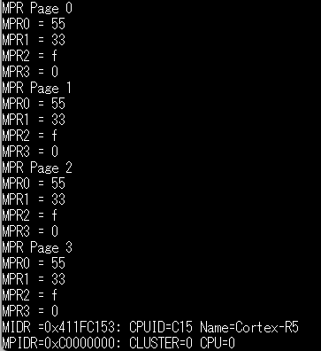
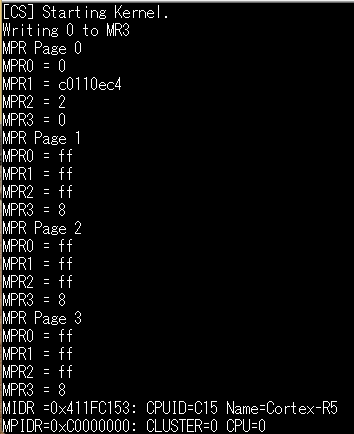
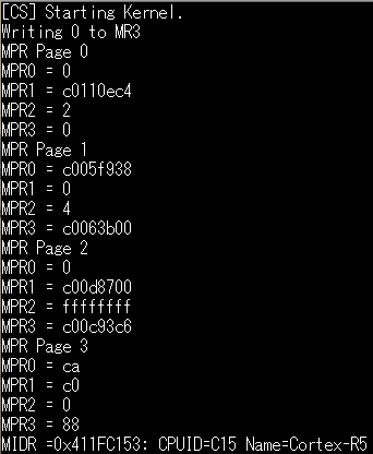
-Get temperature sensor status from the multi-purpose register.
-Process with an interrupt when a CRC error or C/A parity error occurs.
-Set periodic ZQ calibration in DDR.

I checked the AM64x TCR, the AM64x MCU+ SDK documentation, and the DDR4 SDRAM manual, but I can't find a specific method. Please tell me how to do it.

I enabled TCR mode and CA Parity Latency using Sysconfig's DDR Configuration.
Since there is no setting for CRC, I enabled it by directly rewriting the MR2_DATA_F* field of the DDR16SS0_CTL_* register.

I am using Micron DDR4 SDRAM. The model is MT40A1G16TB-062E IT:F.

  • Hello,

    The concerned expert is out of office till June 14th. Please expect a delay in response.

    Regards,

    Nihar Potturu. 

  • These features are currently not supported by the DDR driver or configuration for DDR4.  Are these features a requirement for your product?  I would need some time to investigate if we can enable these.

    Regards,

    James

  • Thank you for your reply.

    All three are requirements, so please investigate.

    Please also let me know how long the investigation will take.

    Also, before investigating, please let me confirm the following three points.

    - Is it not supported to "read values ​​from the multi-purpose register"? Can values ​​other than the temperature sensor status be read from the multi-purpose register?

    - Is there a way to check the ALERT signal from the DDR device (caused by a C/A parity error or CRC error)? (Is this possible by any means other than an interrupt?)

    - Is it not possible to perform "ZQ calibration at any time"?

  • - Is it not supported to "read values ​​from the multi-purpose register"? Can values ​​other than the temperature sensor status be read from the multi-purpose register?

    I believe it should be supported, but this is something outside of normal operation and i just haven't seen anyone try this yet.  Give me some time to try a small test case to ensure it works.

    - Is there a way to check the ALERT signal from the DDR device (caused by a C/A parity error or CRC error)? (Is this possible by any means other than an interrupt?)

    Yes, i believe you should be able to poll an interrupt register.  Again, i have to investigate exactly how to do this.

    - Is it not possible to perform "ZQ calibration at any time"?

    We have periodic ZQ calibration working for LPDDR4, so i believe it should be possible for DDR4 with some configuration changes, we just need time to implement.  

    I will look at these over the next week.  I may need your help to verify some of the implementation.  Do you have a platform to test this out?

    Regards,

    James

  • I have a prototype board for testing.
    The DDR of this prototype board is the same as the EVM board except for the "device shape" and "revision". I confirmed the configuration of the prototype board with the hardware person.

  • A customer has contacted us to confirm the accuracy of the information.
    Please confirm whether the following statements regarding ZQ calibration are correct or incorrect.

    - "Long ZQ calibration" is performed at initialization.
    - Periodic ZQ calibration is "Short ZQ calibration."
    - The default setting is "Perform ZQ calibration at initialization."

  • Yes, these are correct

    Regards,

    James

  • I am able to read the MPR page registers with the following GEL scripts, which should be easily adapted to C code if needed:

    Wait()
    {
        unsigned int i;
        for(i=0;i<10000;i++);
    }
    
    Check_and_Ack_MRW()
    {
        while((HW_RD_REG32(CTL_BASE + DDRSS_CTL_343__SFR_OFFS) & 0x8) == 0x0)
            Wait();
        HW_WR_REG32(CTL_BASE + DDRSS_CTL_351__SFR_OFFS, 0x8); //ack the status mode bit
        Wait();
    }        
            
    hotmenu MPR_read()
    {
        unsigned int mr_addr = 3;
        unsigned int cs = 0;
        unsigned int data,page; 
        unsigned int mpr_bit0,mpr_bit1,mpr_bit2,mpr_bit3,mpr_bit4,mpr_bit5,mpr_bit6,mpr_bit7;
        unsigned int MPR0,MPR1,MPR2,MPR3;
        
        data = 0x24;  //MR3[2] = 1, (Enable MPR data flow)
                      //MR3[12:11] = 0, MPR read format serial
                      //MR3[5] = 1, enable temp sensor
    
        for(page=0;page<3;page++)
        {
            data = (data & ~0x3) | page; //MR3[1:0] = [0-3] MPR page.
    
            //MR write
            HW_WR_REG32(CTL_BASE + DDRSS_CTL_188__SFR_OFFS,((1UL << 23) | (cs << 8) | mr_addr)); 
            Wait();
            HW_WR_REG32(CTL_BASE + DDRSS_CTL_222__SFR_OFFS, data ); 
            //trigger write
            Wait();
            HW_WR_REG32(CTL_BASE + DDRSS_CTL_188__SFR_OFFS, ((1UL << 25) | (1UL << 23) | (cs << 8) | mr_addr)); //set bit 25 to write
            Wait();
            Check_and_Ack_MRW();
            GEL_TextOut("Writing %x to MR%d\n",,,,,data,mr_addr);
    
            
            GEL_TextOut("Reading MPR Page %d Info...\n",,,,,page);
            mpr_bit7 = HW_RD_REG32(0x80000000) & 0x1;
            mpr_bit6 = HW_RD_REG32(0x80000002) & 0x1;
            mpr_bit5 = HW_RD_REG32(0x80000004) & 0x1;
            mpr_bit4 = HW_RD_REG32(0x80000006) & 0x1;
            mpr_bit3 = HW_RD_REG32(0x80000008) & 0x1;
            mpr_bit2 = HW_RD_REG32(0x8000000A) & 0x1;
            mpr_bit1 = HW_RD_REG32(0x8000000C) & 0x1;
            mpr_bit0 = HW_RD_REG32(0x8000000E) & 0x1;
            MPR0 = (mpr_bit7<<7)|(mpr_bit6<<6)|(mpr_bit5<<5)|(mpr_bit4<<4)|(mpr_bit3<<3)|(mpr_bit2<<2)|(mpr_bit1<<1)|(mpr_bit0<<0);
            GEL_TextOut("MPR0 = %x\n",,,,,MPR0);
    
            mpr_bit7 = HW_RD_REG32(0x80001000) & 0x1;
            mpr_bit6 = HW_RD_REG32(0x80001002) & 0x1;
            mpr_bit5 = HW_RD_REG32(0x80001004) & 0x1;
            mpr_bit4 = HW_RD_REG32(0x80001006) & 0x1;
            mpr_bit3 = HW_RD_REG32(0x80001008) & 0x1;
            mpr_bit2 = HW_RD_REG32(0x8000100A) & 0x1;
            mpr_bit1 = HW_RD_REG32(0x8000100C) & 0x1;
            mpr_bit0 = HW_RD_REG32(0x8000100E) & 0x1;
            MPR1 = (mpr_bit7<<7)|(mpr_bit6<<6)|(mpr_bit5<<5)|(mpr_bit4<<4)|(mpr_bit3<<3)|(mpr_bit2<<2)|(mpr_bit1<<1)|(mpr_bit0<<0);
            GEL_TextOut("MPR1 = %x\n",,,,,MPR1);
    
            mpr_bit7 = HW_RD_REG32(0x80002000) & 0x1;
            mpr_bit6 = HW_RD_REG32(0x80002002) & 0x1;
            mpr_bit5 = HW_RD_REG32(0x80002004) & 0x1;
            mpr_bit4 = HW_RD_REG32(0x80002006) & 0x1;
            mpr_bit3 = HW_RD_REG32(0x80002008) & 0x1;
            mpr_bit2 = HW_RD_REG32(0x8000200A) & 0x1;
            mpr_bit1 = HW_RD_REG32(0x8000200C) & 0x1;
            mpr_bit0 = HW_RD_REG32(0x8000200E) & 0x1;
            MPR2 = (mpr_bit7<<7)|(mpr_bit6<<6)|(mpr_bit5<<5)|(mpr_bit4<<4)|(mpr_bit3<<3)|(mpr_bit2<<2)|(mpr_bit1<<1)|(mpr_bit0<<0);
            GEL_TextOut("MPR2 = %x\n",,,,,MPR2);
    
            mpr_bit7 = HW_RD_REG32(0x80002000) & 0x1;
            mpr_bit6 = HW_RD_REG32(0x80002002) & 0x1;
            mpr_bit5 = HW_RD_REG32(0x80002004) & 0x1;
            mpr_bit4 = HW_RD_REG32(0x80002006) & 0x1;
            mpr_bit3 = HW_RD_REG32(0x80002008) & 0x1;
            mpr_bit2 = HW_RD_REG32(0x8000200A) & 0x1;
            mpr_bit1 = HW_RD_REG32(0x8000200C) & 0x1;
            mpr_bit0 = HW_RD_REG32(0x8000200E) & 0x1;
            MPR3 = (mpr_bit7<<7)|(mpr_bit6<<6)|(mpr_bit5<<5)|(mpr_bit4<<4)|(mpr_bit3<<3)|(mpr_bit2<<2)|(mpr_bit1<<1)|(mpr_bit0<<0);
            GEL_TextOut("MPR3 = %x\n",,,,,MPR3);
    
        }
        
        //disable MPR
        data = 0x0;
        
        //MR Write
        HW_WR_REG32(CTL_BASE + DDRSS_CTL_188__SFR_OFFS,((1UL << 23) | (cs << 8) | mr_addr)); 
        Wait();
        HW_WR_REG32(CTL_BASE + DDRSS_CTL_222__SFR_OFFS, data ); 
        //trigger write
        Wait();
        HW_WR_REG32(CTL_BASE + DDRSS_CTL_188__SFR_OFFS, ((1UL << 25) | (1UL << 23) | (cs << 8) | mr_addr)); //set bit 25 to write
        Wait();
        Check_and_Ack_MRW();
        GEL_TextOut("Writing %x to MR%d\n",,,,,data,mr_addr);
    
    }

    The code loops through each of the MPR pages 0-3 (line 27).  The first part of the loop, lines 31-40, writes the appropriate value to MR3 to put the device into MRP access mode.  Then there are four blocks of code to read each of the MPR[0:3] registers as defined in the JEDEC spec.  The temperature sensor status is in MPR Page 2, MPR0.  The access is put into serial mode, so you need to do a series of reads and put the information together as shown on lines 52,63,etc to reveal the register value.  Temp sensor is enabled in the initial write to MR3

    Regards,

    James

  • I rewrote the GEL script into C code and ran it, but it didn't work.

    It seems that writing to MR3 failed because the address is incorrect.

    Please correct the code.

    #include <drivers/hw_include/hw_types.h>
    #include <kernel/dpl/DebugP.h>
    
    #define CTL_BASE 0x0F308000U
    #define DDRSS_CTL_188__SFR_OFFS 0x2F0U
    #define DDRSS_CTL_222__SFR_OFFS 0x378U
    #define DDRSS_CTL_343__SFR_OFFS 0x55CU
    #define DDRSS_CTL_351__SFR_OFFS 0x57CU
    
    void Wait(void)
    {
        unsigned int i;
        for(i=0;i<10000;i++);
    }
    
    void Check_and_Ack_MRW(void)
    {
        while((HW_RD_REG32(CTL_BASE + DDRSS_CTL_343__SFR_OFFS) & 0x8) == 0x0){
            Wait();
    	}
        HW_WR_REG32(CTL_BASE + DDRSS_CTL_351__SFR_OFFS, 0x8); //ack the status mode bit
        Wait();
    } 
    
    void MPR_read(void)
    {
        unsigned int mr_addr = 3;
        unsigned int cs = 0;
        unsigned int data,page; 
        unsigned int mpr_bit0,mpr_bit1,mpr_bit2,mpr_bit3,mpr_bit4,mpr_bit5,mpr_bit6,mpr_bit7;
        unsigned int MPR0,MPR1,MPR2,MPR3;
        
        data = 0x24;  //MR3[2] = 1, (Enable MPR data flow)
                      //MR3[12:11] = 0, MPR read format serial
                      //MR3[5] = 1, enable temp sensor
    
        for(page=0;page<3;page++)
        {
            data = (data & ~0x3) | page; //MR3[1:0] = [0-3] MPR page.
            //MR write
            HW_WR_REG32(CTL_BASE + DDRSS_CTL_188__SFR_OFFS,((1UL << 23) | (cs << 8) | mr_addr)); 
            Wait();
            HW_WR_REG32(CTL_BASE + DDRSS_CTL_222__SFR_OFFS, data ); 
            //trigger write
            Wait();
            HW_WR_REG32(CTL_BASE + DDRSS_CTL_188__SFR_OFFS, ((1UL << 25) | (1UL << 23) | (cs << 8) | mr_addr)); //set bit 25 to write
            Wait();
            Check_and_Ack_MRW();
            DebugP_log("Writing %x to MR%d\n",data,mr_addr);
    
            
            DebugP_log("Reading MPR Page %d Info...\n",page);
            mpr_bit7 = HW_RD_REG32(0x80000000) & 0x1;
            mpr_bit6 = HW_RD_REG32(0x80000002) & 0x1;
            mpr_bit5 = HW_RD_REG32(0x80000004) & 0x1;
            mpr_bit4 = HW_RD_REG32(0x80000006) & 0x1;
            mpr_bit3 = HW_RD_REG32(0x80000008) & 0x1;
            mpr_bit2 = HW_RD_REG32(0x8000000A) & 0x1;
            mpr_bit1 = HW_RD_REG32(0x8000000C) & 0x1;
            mpr_bit0 = HW_RD_REG32(0x8000000E) & 0x1;
            MPR0 = (mpr_bit7<<7)|(mpr_bit6<<6)|(mpr_bit5<<5)|(mpr_bit4<<4)|(mpr_bit3<<3)|(mpr_bit2<<2)|(mpr_bit1<<1)|(mpr_bit0<<0);
            DebugP_log("MPR0 = %x\n",MPR0);
    
            mpr_bit7 = HW_RD_REG32(0x80001000) & 0x1;
            mpr_bit6 = HW_RD_REG32(0x80001002) & 0x1;
            mpr_bit5 = HW_RD_REG32(0x80001004) & 0x1;
            mpr_bit4 = HW_RD_REG32(0x80001006) & 0x1;
            mpr_bit3 = HW_RD_REG32(0x80001008) & 0x1;
            mpr_bit2 = HW_RD_REG32(0x8000100A) & 0x1;
            mpr_bit1 = HW_RD_REG32(0x8000100C) & 0x1;
            mpr_bit0 = HW_RD_REG32(0x8000100E) & 0x1;
            MPR1 = (mpr_bit7<<7)|(mpr_bit6<<6)|(mpr_bit5<<5)|(mpr_bit4<<4)|(mpr_bit3<<3)|(mpr_bit2<<2)|(mpr_bit1<<1)|(mpr_bit0<<0);
            DebugP_log("MPR1 = %x\n",MPR1);
    
            mpr_bit7 = HW_RD_REG32(0x80002000) & 0x1;
            mpr_bit6 = HW_RD_REG32(0x80002002) & 0x1;
            mpr_bit5 = HW_RD_REG32(0x80002004) & 0x1;
            mpr_bit4 = HW_RD_REG32(0x80002006) & 0x1;
            mpr_bit3 = HW_RD_REG32(0x80002008) & 0x1;
            mpr_bit2 = HW_RD_REG32(0x8000200A) & 0x1;
            mpr_bit1 = HW_RD_REG32(0x8000200C) & 0x1;
            mpr_bit0 = HW_RD_REG32(0x8000200E) & 0x1;
            MPR2 = (mpr_bit7<<7)|(mpr_bit6<<6)|(mpr_bit5<<5)|(mpr_bit4<<4)|(mpr_bit3<<3)|(mpr_bit2<<2)|(mpr_bit1<<1)|(mpr_bit0<<0);
            DebugP_log("MPR2 = %x\n",MPR2);
    
            mpr_bit7 = HW_RD_REG32(0x80002000) & 0x1;
            mpr_bit6 = HW_RD_REG32(0x80002002) & 0x1;
            mpr_bit5 = HW_RD_REG32(0x80002004) & 0x1;
            mpr_bit4 = HW_RD_REG32(0x80002006) & 0x1;
            mpr_bit3 = HW_RD_REG32(0x80002008) & 0x1;
            mpr_bit2 = HW_RD_REG32(0x8000200A) & 0x1;
            mpr_bit1 = HW_RD_REG32(0x8000200C) & 0x1;
            mpr_bit0 = HW_RD_REG32(0x8000200E) & 0x1;
            MPR3 = (mpr_bit7<<7)|(mpr_bit6<<6)|(mpr_bit5<<5)|(mpr_bit4<<4)|(mpr_bit3<<3)|(mpr_bit2<<2)|(mpr_bit1<<1)|(mpr_bit0<<0);
            DebugP_log("MPR3 = %x\n",MPR3);
    
        }
        
        //disable MPR
        data = 0x0;
        
        //MR Write
        HW_WR_REG32(CTL_BASE + DDRSS_CTL_188__SFR_OFFS,((1UL << 23) | (cs << 8) | mr_addr)); 
        Wait();
        HW_WR_REG32(CTL_BASE + DDRSS_CTL_222__SFR_OFFS, data ); 
        //trigger write
        Wait();
        HW_WR_REG32(CTL_BASE + DDRSS_CTL_188__SFR_OFFS, ((1UL << 25) | (1UL << 23) | (cs << 8) | mr_addr)); //set bit 25 to write
        Wait();
        Check_and_Ack_MRW();
        DebugP_log("Writing %x to MR%d\n",data,mr_addr);
    
    }

  • Takeshi,

    Did you initialize the memory first?  Your code looks correct, i don't see any issues with it.  Did the code get stuck in one of the loops?  Can you ensure the CTL registers are getting written correctly?

    Regards,

    James

  • DDR_init was not executed during the initialization process, so I corrected the code.
    However, even after making this correction, it still does not work properly.
    The behavior seems to be due to a problem somewhere other than this code, so please advise where I should check.

    Using a debugger, I confirmed that the destination address and value are correct in the following two places.

    Line 41: The value 0x00800003 was written to address 0x0F3082F0.
    Line 43: The value 0x00000024 was written to address 0x0F308378.

    The write on line 46 was not performed correctly.
    When I step through these lines with the debugger, for some reason it jumps to the RTOS code instead of line 47.
    If I continue executing after that, an undefined instruction exception will occur.

  • I believe line 46 may not completely reflect in the register, as i believe the bit will self clear.  What do you mean by "RTOS code"?  Are you landing up in an interrupt service routine?  An interrupt will be triggered by the write if the appropriate mask bits are set correctly.  Can you "step over" line 46 to get through the ISR if that is what it is?

    Regards,

    James

  • The code that reads the MPR from DDR is executed when the main task of a TOPPER RTOS is started.

    "RTOS code" means "assembler code that is part of the RTOS."

    I checked where in this assembler code it was jumping to. When I "Step Into" from line 46, it went to "UndefinedHandler".

  • Oh!  This code needs to be run from internal memory, because the switch over to access the MPR registers takes over the whole data bus.  Memory data will be inaccessible until MPR read mode is disabled.  That's probably why you are getting an UndefinedHandler error.

    Regards,

    James

  • I now understand why the error was occurring.
    The MPR block diagram shows the operation of "changing the mode register to switch the bus to the memory core to the bus to the MPR."
    I understand that the code was executed successfully up to line 46, but as a result, the area where the code is located became inaccessible, causing the error.

    The customer's request is to "obtain the refresh rate for Temperature-Controlled Refresh."
    Is there any way to achieve this other than "accessing the MPR register"?
    I don't think there is, but if there is, I would like to use it, so please let me confirm.

  • No, on DDR4, the only way to get this info is through MPR registers.  LPDDR4 devices have a less intrusive way to control refresh rate.

    Regards,

    James

  • After moving the code to MSRAM, execution is now progressing to a certain extent.

    The current code is as follows.

    I was able to confirm using the debugger that Check_and_Ack_MRW() completes once, but an undefined instruction exception occurs when reading the MPR on line 69.

    I would appreciate some advice on how to resolve this.

    #include <drivers/hw_include/hw_types.h>
    #include <kernel/dpl/DebugP.h>
    #include <kernel/dpl/AddrTranslateP.h>
    
    #define CTL_BASE 0x0F308000U
    #define DDRSS_CTL_188__SFR_OFFS 0x2F0U
    #define DDRSS_CTL_222__SFR_OFFS 0x378U
    #define DDRSS_CTL_343__SFR_OFFS 0x55CU
    #define DDRSS_CTL_351__SFR_OFFS 0x57CU
    
    __attribute__((section(".mpr_sec"))) uint32_t HW_WR_REG32_MPR(uint32_t addr)
    {
    	uint32_t regVal = *(volatile uint32_t *)((uintptr_t)addr);
    	return (regVal);
    }
    
    __attribute__((section(".mpr_sec"))) void HW_WR_REG32_MPR_CHK(uint32_t addr, uint32_t value)
    {
    	*(volatile uint32_t *)((uintptr_t)addr) = value;
    	return;
    }
    
    __attribute__((section(".mpr_sec"))) void Wait(void)
    {
        unsigned int i;
        for(i=0;i<10000;i++);
    }
    
    __attribute__((section(".mpr_sec"))) void Check_and_Ack_MRW(void)
    {
    	//while ((HW_RD_REG32(CTL_BASE + DDRSS_CTL_343__SFR_OFFS) & 0x8) == 0x0)
    	while ((HW_WR_REG32_MPR(0x0F308000U + 0x55CU) & 0x8) == 0x0)
    	{
            Wait();
    	}
    	//HW_WR_REG32(CTL_BASE + DDRSS_CTL_351__SFR_OFFS, 0x8); // ack the status mode bit
    	HW_WR_REG32_MPR_CHK(0x0F308000U + 0x57CU, 0x8); // ack the status mode bit
        Wait();
    } 
    
    __attribute__((section(".mpr_sec"))) void MPR_read(void)
    {
        unsigned int mr_addr = 3;
        unsigned int cs = 0;
        unsigned int data,page; 
        unsigned int mpr_bit0,mpr_bit1,mpr_bit2,mpr_bit3,mpr_bit4,mpr_bit5,mpr_bit6,mpr_bit7;
        unsigned int MPR0,MPR1,MPR2,MPR3;
        
        data = 0x24;  //MR3[2] = 1, (Enable MPR data flow)
                      //MR3[12:11] = 0, MPR read format serial
                      //MR3[5] = 1, enable temp sensor
    
        for(page=0;page<3;page++)
        {
            data = (data & ~0x3) | page; //MR3[1:0] = [0-3] MPR page.
            //MR write
    		HW_WR_REG32(CTL_BASE + DDRSS_CTL_188__SFR_OFFS, ((1UL << 23) | (cs << 8) | mr_addr));
            Wait();
    		HW_WR_REG32(CTL_BASE + DDRSS_CTL_222__SFR_OFFS, data);
            //trigger write
            Wait();
    		HW_WR_REG32(CTL_BASE + DDRSS_CTL_188__SFR_OFFS, ((1UL << 25) | (1UL << 23) | (cs << 8) | mr_addr)); // set bit 25 to write
            Wait();
            Check_and_Ack_MRW();
            //DebugP_log("Writing %x to MR%d\n",data,mr_addr);
    
            
            //DebugP_log("Reading MPR Page %d Info...\n",page);
            mpr_bit7 = HW_WR_REG32_MPR(0x80000000) & 0x1;
            mpr_bit6 = HW_WR_REG32_MPR(0x80000002) & 0x1;
            mpr_bit5 = HW_WR_REG32_MPR(0x80000004) & 0x1;
            mpr_bit4 = HW_WR_REG32_MPR(0x80000006) & 0x1;
            mpr_bit3 = HW_WR_REG32_MPR(0x80000008) & 0x1;
            mpr_bit2 = HW_WR_REG32_MPR(0x8000000A) & 0x1;
            mpr_bit1 = HW_WR_REG32_MPR(0x8000000C) & 0x1;
            mpr_bit0 = HW_WR_REG32_MPR(0x8000000E) & 0x1;
            MPR0 = (mpr_bit7<<7)|(mpr_bit6<<6)|(mpr_bit5<<5)|(mpr_bit4<<4)|(mpr_bit3<<3)|(mpr_bit2<<2)|(mpr_bit1<<1)|(mpr_bit0<<0);
            //DebugP_log("MPR0 = %x\n",MPR0);
    
            mpr_bit7 = HW_WR_REG32_MPR(0x80001000) & 0x1;
            mpr_bit6 = HW_WR_REG32_MPR(0x80001002) & 0x1;
            mpr_bit5 = HW_WR_REG32_MPR(0x80001004) & 0x1;
            mpr_bit4 = HW_WR_REG32_MPR(0x80001006) & 0x1;
            mpr_bit3 = HW_WR_REG32_MPR(0x80001008) & 0x1;
            mpr_bit2 = HW_WR_REG32_MPR(0x8000100A) & 0x1;
            mpr_bit1 = HW_WR_REG32_MPR(0x8000100C) & 0x1;
            mpr_bit0 = HW_WR_REG32_MPR(0x8000100E) & 0x1;
            MPR1 = (mpr_bit7<<7)|(mpr_bit6<<6)|(mpr_bit5<<5)|(mpr_bit4<<4)|(mpr_bit3<<3)|(mpr_bit2<<2)|(mpr_bit1<<1)|(mpr_bit0<<0);
            //DebugP_log("MPR1 = %x\n",MPR1);
    
            mpr_bit7 = HW_WR_REG32_MPR(0x80002000) & 0x1;
            mpr_bit6 = HW_WR_REG32_MPR(0x80002002) & 0x1;
            mpr_bit5 = HW_WR_REG32_MPR(0x80002004) & 0x1;
            mpr_bit4 = HW_WR_REG32_MPR(0x80002006) & 0x1;
            mpr_bit3 = HW_WR_REG32_MPR(0x80002008) & 0x1;
            mpr_bit2 = HW_WR_REG32_MPR(0x8000200A) & 0x1;
            mpr_bit1 = HW_WR_REG32_MPR(0x8000200C) & 0x1;
            mpr_bit0 = HW_WR_REG32_MPR(0x8000200E) & 0x1;
            MPR2 = (mpr_bit7<<7)|(mpr_bit6<<6)|(mpr_bit5<<5)|(mpr_bit4<<4)|(mpr_bit3<<3)|(mpr_bit2<<2)|(mpr_bit1<<1)|(mpr_bit0<<0);
            //DebugP_log("MPR2 = %x\n",MPR2);
    
            mpr_bit7 = HW_WR_REG32_MPR(0x80002000) & 0x1;
            mpr_bit6 = HW_WR_REG32_MPR(0x80002002) & 0x1;
            mpr_bit5 = HW_WR_REG32_MPR(0x80002004) & 0x1;
            mpr_bit4 = HW_WR_REG32_MPR(0x80002006) & 0x1;
            mpr_bit3 = HW_WR_REG32_MPR(0x80002008) & 0x1;
            mpr_bit2 = HW_WR_REG32_MPR(0x8000200A) & 0x1;
            mpr_bit1 = HW_WR_REG32_MPR(0x8000200C) & 0x1;
            mpr_bit0 = HW_WR_REG32_MPR(0x8000200E) & 0x1;
            MPR3 = (mpr_bit7<<7)|(mpr_bit6<<6)|(mpr_bit5<<5)|(mpr_bit4<<4)|(mpr_bit3<<3)|(mpr_bit2<<2)|(mpr_bit1<<1)|(mpr_bit0<<0);
            //DebugP_log("MPR3 = %x\n",MPR3);
    
        }
        
        //disable MPR
        data = 0x0;
        
        //MR Write
        HW_WR_REG32(CTL_BASE + DDRSS_CTL_188__SFR_OFFS,((1UL << 23) | (cs << 8) | mr_addr)); 
        Wait();
        HW_WR_REG32(CTL_BASE + DDRSS_CTL_222__SFR_OFFS, data ); 
        //trigger write
        Wait();
        HW_WR_REG32(CTL_BASE + DDRSS_CTL_188__SFR_OFFS, ((1UL << 25) | (1UL << 23) | (cs << 8) | mr_addr)); //set bit 25 to write
        Wait();
        Check_and_Ack_MRW();
        //DebugP_log("Writing %x to MR%d\n",data,mr_addr);
    
    }

  • You have HW_WR_REG32_MPR() on line 69.  It should be a read function

    Regards,

    James

  • I changed HW_WR_REG32_MPR to HW_RD_REG32_MPR and ran it, but an undefined instruction exception occurs on the same line.

    After tracing the location of the error in detail with a debugger, I found that the undefined instruction exception occurs on the line (line 13) that reads the register in HW_RD_REG32_MPR().

    I would also appreciate some advice on how to resolve this.

    #include <drivers/hw_include/hw_types.h>
    #include <kernel/dpl/DebugP.h>
    #include <kernel/dpl/AddrTranslateP.h>
    
    #define CTL_BASE 0x0F308000U
    #define DDRSS_CTL_188__SFR_OFFS 0x2F0U
    #define DDRSS_CTL_222__SFR_OFFS 0x378U
    #define DDRSS_CTL_343__SFR_OFFS 0x55CU
    #define DDRSS_CTL_351__SFR_OFFS 0x57CU
    
    __attribute__((section(".mpr_sec"))) uint32_t HW_RD_REG32_MPR(uint32_t addr)
    {
    	uint32_t regVal = *(volatile uint32_t *)((uintptr_t)addr);
    	return (regVal);
    }
    
    __attribute__((section(".mpr_sec"))) void HW_WR_REG32_MPR(uint32_t addr, uint32_t value)
    {
    	*(volatile uint32_t *)((uintptr_t)addr) = value;
    	return;
    }
    
    __attribute__((section(".mpr_sec"))) void Wait(void)
    {
        unsigned int i;
        for(i=0;i<10000;i++);
    }
    
    __attribute__((section(".mpr_sec"))) void Check_and_Ack_MRW(void)
    {
    	//while ((HW_RD_REG32(CTL_BASE + DDRSS_CTL_343__SFR_OFFS) & 0x8) == 0x0)
    	while ((HW_RD_REG32_MPR(0x0F308000U + 0x55CU) & 0x8) == 0x0)
    	{
            Wait();
    	}
    	//HW_WR_REG32(CTL_BASE + DDRSS_CTL_351__SFR_OFFS, 0x8); // ack the status mode bit
    	HW_WR_REG32_MPR(0x0F308000U + 0x57CU, 0x8); // ack the status mode bit
        Wait();
    } 
    
    __attribute__((section(".mpr_sec"))) void MPR_read(void)
    {
        unsigned int mr_addr = 3;
        unsigned int cs = 0;
        unsigned int data,page; 
        unsigned int mpr_bit0,mpr_bit1,mpr_bit2,mpr_bit3,mpr_bit4,mpr_bit5,mpr_bit6,mpr_bit7;
        unsigned int MPR0,MPR1,MPR2,MPR3;
        
        data = 0x24;  //MR3[2] = 1, (Enable MPR data flow)
                      //MR3[12:11] = 0, MPR read format serial
                      //MR3[5] = 1, enable temp sensor
    
        for(page=0;page<3;page++)
        {
            data = (data & ~0x3) | page; //MR3[1:0] = [0-3] MPR page.
            //MR write
    		// HW_WR_REG32_MPR(CTL_BASE + DDRSS_CTL_188__SFR_OFFS, ((1UL << 23) | (cs << 8) | mr_addr));
    		HW_WR_REG32_MPR(0x0F308000U + 0x2F0U, ((1UL << 23) | (cs << 8) | mr_addr));
            Wait();
    		// HW_WR_REG32_MPR(CTL_BASE + DDRSS_CTL_222__SFR_OFFS, data);
    		HW_WR_REG32_MPR(0x0F308000U + 0x378U, data);
            //trigger write
            Wait();
    		//HW_WR_REG32(CTL_BASE + DDRSS_CTL_188__SFR_OFFS, ((1UL << 25) | (1UL << 23) | (cs << 8) | mr_addr)); // set bit 25 to write
    		HW_WR_REG32_MPR(0x0F308000U + 0x2F0U, ((1UL << 25) | (1UL << 23) | (cs << 8) | mr_addr)); // set bit 25 to write
            Wait();
            Check_and_Ack_MRW();
            //DebugP_log("Writing %x to MR%d\n",data,mr_addr);
    
            
            //DebugP_log("Reading MPR Page %d Info...\n",page);
    		mpr_bit7 = HW_RD_REG32_MPR(0x80000000) & 0x1;
    		mpr_bit6 = HW_RD_REG32_MPR(0x80000002) & 0x1;
    		mpr_bit5 = HW_RD_REG32_MPR(0x80000004) & 0x1;
    		mpr_bit4 = HW_RD_REG32_MPR(0x80000006) & 0x1;
    		mpr_bit3 = HW_RD_REG32_MPR(0x80000008) & 0x1;
    		mpr_bit2 = HW_RD_REG32_MPR(0x8000000A) & 0x1;
    		mpr_bit1 = HW_RD_REG32_MPR(0x8000000C) & 0x1;
    		mpr_bit0 = HW_RD_REG32_MPR(0x8000000E) & 0x1;
            MPR0 = (mpr_bit7<<7)|(mpr_bit6<<6)|(mpr_bit5<<5)|(mpr_bit4<<4)|(mpr_bit3<<3)|(mpr_bit2<<2)|(mpr_bit1<<1)|(mpr_bit0<<0);
            //DebugP_log("MPR0 = %x\n",MPR0);
    
    		mpr_bit7 = HW_RD_REG32_MPR(0x80001000) & 0x1;
    		mpr_bit6 = HW_RD_REG32_MPR(0x80001002) & 0x1;
    		mpr_bit5 = HW_RD_REG32_MPR(0x80001004) & 0x1;
    		mpr_bit4 = HW_RD_REG32_MPR(0x80001006) & 0x1;
    		mpr_bit3 = HW_RD_REG32_MPR(0x80001008) & 0x1;
    		mpr_bit2 = HW_RD_REG32_MPR(0x8000100A) & 0x1;
    		mpr_bit1 = HW_RD_REG32_MPR(0x8000100C) & 0x1;
    		mpr_bit0 = HW_RD_REG32_MPR(0x8000100E) & 0x1;
            MPR1 = (mpr_bit7<<7)|(mpr_bit6<<6)|(mpr_bit5<<5)|(mpr_bit4<<4)|(mpr_bit3<<3)|(mpr_bit2<<2)|(mpr_bit1<<1)|(mpr_bit0<<0);
            //DebugP_log("MPR1 = %x\n",MPR1);
    
    		mpr_bit7 = HW_RD_REG32_MPR(0x80002000) & 0x1;
    		mpr_bit6 = HW_RD_REG32_MPR(0x80002002) & 0x1;
    		mpr_bit5 = HW_RD_REG32_MPR(0x80002004) & 0x1;
    		mpr_bit4 = HW_RD_REG32_MPR(0x80002006) & 0x1;
    		mpr_bit3 = HW_RD_REG32_MPR(0x80002008) & 0x1;
    		mpr_bit2 = HW_RD_REG32_MPR(0x8000200A) & 0x1;
    		mpr_bit1 = HW_RD_REG32_MPR(0x8000200C) & 0x1;
    		mpr_bit0 = HW_RD_REG32_MPR(0x8000200E) & 0x1;
            MPR2 = (mpr_bit7<<7)|(mpr_bit6<<6)|(mpr_bit5<<5)|(mpr_bit4<<4)|(mpr_bit3<<3)|(mpr_bit2<<2)|(mpr_bit1<<1)|(mpr_bit0<<0);
            //DebugP_log("MPR2 = %x\n",MPR2);
    
    		mpr_bit7 = HW_RD_REG32_MPR(0x80002000) & 0x1;
    		mpr_bit6 = HW_RD_REG32_MPR(0x80002002) & 0x1;
    		mpr_bit5 = HW_RD_REG32_MPR(0x80002004) & 0x1;
    		mpr_bit4 = HW_RD_REG32_MPR(0x80002006) & 0x1;
    		mpr_bit3 = HW_RD_REG32_MPR(0x80002008) & 0x1;
    		mpr_bit2 = HW_RD_REG32_MPR(0x8000200A) & 0x1;
    		mpr_bit1 = HW_RD_REG32_MPR(0x8000200C) & 0x1;
    		mpr_bit0 = HW_RD_REG32_MPR(0x8000200E) & 0x1;
            MPR3 = (mpr_bit7<<7)|(mpr_bit6<<6)|(mpr_bit5<<5)|(mpr_bit4<<4)|(mpr_bit3<<3)|(mpr_bit2<<2)|(mpr_bit1<<1)|(mpr_bit0<<0);
            //DebugP_log("MPR3 = %x\n",MPR3);
    		
        }
        
        //disable MPR
        data = 0x0;
        
        //MR Write
        //HW_WR_REG32(CTL_BASE + DDRSS_CTL_188__SFR_OFFS,((1UL << 23) | (cs << 8) | mr_addr)); 
    	HW_WR_REG32(0x0F308000U + 0x2F0U, ((1UL << 23) | (cs << 8) | mr_addr));
        Wait();
        //HW_WR_REG32(CTL_BASE + DDRSS_CTL_222__SFR_OFFS, data ); 
    	HW_WR_REG32(0x0F308000U + 0x378U, data);
        //trigger write
        Wait();
        //HW_WR_REG32(CTL_BASE + DDRSS_CTL_188__SFR_OFFS, ((1UL << 25) | (1UL << 23) | (cs << 8) | mr_addr)); //set bit 25 to write
    	HW_WR_REG32(0x0F308000U + 0x2F0U, ((1UL << 25) | (1UL << 23) | (cs << 8) | mr_addr)); // set bit 25 to write
        Wait();
        Check_and_Ack_MRW();
        //DebugP_log("Writing %x to MR%d\n",data,mr_addr);
    
    }

  • Does that function work even without switching to MPR mode?  Can you perform a dummy read of 0x80000000 at the very beginning of the test, before you get into MPR mode?  Also, can you read from 0x80000000 in a memory browser in the debugger? It should simply read the value out of address 0x80000000.  If that doesn't work, maybe you are not truly reading from the address.  You might need to step through the assembly code to ensure it is reading from that address.  

    Which processor core are you running this code from?  

    Regards,

    James

  • The results for each of the three checks were as follows.

    >Does this function work without switching to MPR mode? Can you perform a dummy read of 0x80000000 at the beginning of the test, before entering MPR mode?
    →I executed the function HW_RD_REG32_MPR(0x80000000) before entering the for loop, but it does not work properly. A Data Abort Exception occurs.

    >Also, can you read from 0x80000000 in the debugger's memory browser?
    →Immediately after debugging, the memory from 0x80000000 is displayed. However, when the function System_init is executed, this part is displayed as "????".

    >Which processor core is this code running on?
    →It is running on the R5F0-0 core.

  • I'm not sure what your full environment is, but if you are working from the MCU+ SDK, System_Init initializes the DDR. 

    It seems like you added DDR_init earlier, and then System_Init is trying to reinitialize the DDR, which is not allowed.  You should only init the DDR once.

    Step into System_init while the memory browser is open to see which instruction the memory browser starts showing ????

    Regards,

    James

  • DDR_init is currently set to run only once.

    Immediately after launch, I performed step execution to check at which line the display at 0x80000000 changed to "????".
    The display changed when the MPU was enabled. When I checked the MPU settings, I found that the area after 0x80000000 was not defined.
    Adding the MPU settings enabled me to read all of page 0 of the MPR, but I was unable to read pages 1 and beyond.

  • Page 0 vs page 1,2,3 is just a setting in MR3, which is taken care of by the for() loop.  Ensure that is working correctly, so that MR3[1:0] changes from 0,1,2,3 each time through the loop

    Also, maybe put a delay at the end of the for() loop.  There might be some timing issue reading from page to page.

    Regards,

    James

  • By inserting Wait() at the end of the for() loop, I was able to run it without stopping.
    When I checked the change in the page variable in the for() loop, I found that the loop ended before it became 3, so I changed the condition expression to "page<=3".

    #include <drivers/hw_include/hw_types.h>
    #include <kernel/dpl/DebugP.h>
    #include <kernel/dpl/AddrTranslateP.h>
    
    #define CTL_BASE 0x0F308000U
    #define DDRSS_CTL_188__SFR_OFFS 0x2F0U
    #define DDRSS_CTL_222__SFR_OFFS 0x378U
    #define DDRSS_CTL_343__SFR_OFFS 0x55CU
    #define DDRSS_CTL_351__SFR_OFFS 0x57CU
    
    __attribute__((section(".mpr_sec"))) uint32_t HW_RD_REG32_MPR(uint32_t addr)
    {
    	uint32_t regVal = *(volatile uint32_t *)((uintptr_t)addr);
    	return (regVal);
    }
    
    __attribute__((section(".mpr_sec"))) void HW_WR_REG32_MPR(uint32_t addr, uint32_t value)
    {
    	*(volatile uint32_t *)((uintptr_t)addr) = value;
    	return;
    }
    
    __attribute__((section(".mpr_sec"))) void Wait(void)
    {
        unsigned int i;
        for(i=0;i<10000;i++);
    }
    
    __attribute__((section(".mpr_sec"))) void Check_and_Ack_MRW(void)
    {
    	//while ((HW_RD_REG32(CTL_BASE + DDRSS_CTL_343__SFR_OFFS) & 0x8) == 0x0)
    	while ((HW_RD_REG32_MPR(0x0F308000U + 0x55CU) & 0x8) == 0x0)
    	{
            Wait();
    	}
    	//HW_WR_REG32(CTL_BASE + DDRSS_CTL_351__SFR_OFFS, 0x8); // ack the status mode bit
    	HW_WR_REG32_MPR(0x0F308000U + 0x57CU, 0x8); // ack the status mode bit
        Wait();
    } 
    
    __attribute__((section(".mpr_sec"))) void MPR_read(void)
    {
        unsigned int mr_addr = 3;
        unsigned int cs = 0;
        unsigned int data,page; 
        unsigned int mpr_bit0,mpr_bit1,mpr_bit2,mpr_bit3,mpr_bit4,mpr_bit5,mpr_bit6,mpr_bit7;
        unsigned int MPR0,MPR1,MPR2,MPR3;
        
        data = 0x24;  //MR3[2] = 1, (Enable MPR data flow)
                      //MR3[12:11] = 0, MPR read format serial
                      //MR3[5] = 1, enable temp sensor
    
    	mpr_bit7 = HW_RD_REG32_MPR(0x80000000) & 0x1;
    	DebugP_log("mpr_bit7 %d\n" ,data);
    
        for(page=0;page<=3;page++)
        {
            data = (data & ~0x3) | page; //MR3[1:0] = [0-3] MPR page.
            //MR write
    		// HW_WR_REG32_MPR(CTL_BASE + DDRSS_CTL_188__SFR_OFFS, ((1UL << 23) | (cs << 8) | mr_addr));
    		HW_WR_REG32_MPR(0x0F308000U + 0x2F0U, ((1UL << 23) | (cs << 8) | mr_addr));
            Wait();
    		// HW_WR_REG32_MPR(CTL_BASE + DDRSS_CTL_222__SFR_OFFS, data);
    		HW_WR_REG32_MPR(0x0F308000U + 0x378U, data);
            //trigger write
            Wait();
    		//HW_WR_REG32(CTL_BASE + DDRSS_CTL_188__SFR_OFFS, ((1UL << 25) | (1UL << 23) | (cs << 8) | mr_addr)); // set bit 25 to write
    		HW_WR_REG32_MPR(0x0F308000U + 0x2F0U, ((1UL << 25) | (1UL << 23) | (cs << 8) | mr_addr)); // set bit 25 to write
            Wait();
            Check_and_Ack_MRW();
            //DebugP_log("Writing %x to MR%d\n",data,mr_addr);
    
            
            //DebugP_log("Reading MPR Page %d Info...\n",page);
    		mpr_bit7 = HW_RD_REG32_MPR(0x80000000) & 0x1;
    		mpr_bit6 = HW_RD_REG32_MPR(0x80000002) & 0x1;
    		mpr_bit5 = HW_RD_REG32_MPR(0x80000004) & 0x1;
    		mpr_bit4 = HW_RD_REG32_MPR(0x80000006) & 0x1;
    		mpr_bit3 = HW_RD_REG32_MPR(0x80000008) & 0x1;
    		mpr_bit2 = HW_RD_REG32_MPR(0x8000000A) & 0x1;
    		mpr_bit1 = HW_RD_REG32_MPR(0x8000000C) & 0x1;
    		mpr_bit0 = HW_RD_REG32_MPR(0x8000000E) & 0x1;
            MPR0 = (mpr_bit7<<7)|(mpr_bit6<<6)|(mpr_bit5<<5)|(mpr_bit4<<4)|(mpr_bit3<<3)|(mpr_bit2<<2)|(mpr_bit1<<1)|(mpr_bit0<<0);
            //DebugP_log("MPR0 = %x\n",MPR0);
    
    		mpr_bit7 = HW_RD_REG32_MPR(0x80001000) & 0x1;
    		mpr_bit6 = HW_RD_REG32_MPR(0x80001002) & 0x1;
    		mpr_bit5 = HW_RD_REG32_MPR(0x80001004) & 0x1;
    		mpr_bit4 = HW_RD_REG32_MPR(0x80001006) & 0x1;
    		mpr_bit3 = HW_RD_REG32_MPR(0x80001008) & 0x1;
    		mpr_bit2 = HW_RD_REG32_MPR(0x8000100A) & 0x1;
    		mpr_bit1 = HW_RD_REG32_MPR(0x8000100C) & 0x1;
    		mpr_bit0 = HW_RD_REG32_MPR(0x8000100E) & 0x1;
            MPR1 = (mpr_bit7<<7)|(mpr_bit6<<6)|(mpr_bit5<<5)|(mpr_bit4<<4)|(mpr_bit3<<3)|(mpr_bit2<<2)|(mpr_bit1<<1)|(mpr_bit0<<0);
            //DebugP_log("MPR1 = %x\n",MPR1);
    		
    		mpr_bit7 = HW_RD_REG32_MPR(0x80002000) & 0x1;
    		mpr_bit6 = HW_RD_REG32_MPR(0x80002002) & 0x1;
    		mpr_bit5 = HW_RD_REG32_MPR(0x80002004) & 0x1;
    		mpr_bit4 = HW_RD_REG32_MPR(0x80002006) & 0x1;
    		mpr_bit3 = HW_RD_REG32_MPR(0x80002008) & 0x1;
    		mpr_bit2 = HW_RD_REG32_MPR(0x8000200A) & 0x1;
    		mpr_bit1 = HW_RD_REG32_MPR(0x8000200C) & 0x1;
    		mpr_bit0 = HW_RD_REG32_MPR(0x8000200E) & 0x1;
            MPR2 = (mpr_bit7<<7)|(mpr_bit6<<6)|(mpr_bit5<<5)|(mpr_bit4<<4)|(mpr_bit3<<3)|(mpr_bit2<<2)|(mpr_bit1<<1)|(mpr_bit0<<0);
            //DebugP_log("MPR2 = %x\n",MPR2);
    
    		mpr_bit7 = HW_RD_REG32_MPR(0x80002000) & 0x1;
    		mpr_bit6 = HW_RD_REG32_MPR(0x80002002) & 0x1;
    		mpr_bit5 = HW_RD_REG32_MPR(0x80002004) & 0x1;
    		mpr_bit4 = HW_RD_REG32_MPR(0x80002006) & 0x1;
    		mpr_bit3 = HW_RD_REG32_MPR(0x80002008) & 0x1;
    		mpr_bit2 = HW_RD_REG32_MPR(0x8000200A) & 0x1;
    		mpr_bit1 = HW_RD_REG32_MPR(0x8000200C) & 0x1;
    		mpr_bit0 = HW_RD_REG32_MPR(0x8000200E) & 0x1;
            MPR3 = (mpr_bit7<<7)|(mpr_bit6<<6)|(mpr_bit5<<5)|(mpr_bit4<<4)|(mpr_bit3<<3)|(mpr_bit2<<2)|(mpr_bit1<<1)|(mpr_bit0<<0);
            //DebugP_log("MPR3 = %x\n",MPR3);
    
    		Wait();
        }
        
        //disable MPR
        data = 0x0;
        
        //MR Write
        //HW_WR_REG32(CTL_BASE + DDRSS_CTL_188__SFR_OFFS,((1UL << 23) | (cs << 8) | mr_addr)); 
    	HW_WR_REG32_MPR(0x0F308000U + 0x2F0U, ((1UL << 23) | (cs << 8) | mr_addr));
        Wait();
        //HW_WR_REG32(CTL_BASE + DDRSS_CTL_222__SFR_OFFS, data ); 
    	HW_WR_REG32_MPR(0x0F308000U + 0x378U, data);
        //trigger write
        Wait();
        //HW_WR_REG32(CTL_BASE + DDRSS_CTL_188__SFR_OFFS, ((1UL << 25) | (1UL << 23) | (cs << 8) | mr_addr)); //set bit 25 to write
    	HW_WR_REG32_MPR(0x0F308000U + 0x2F0U, ((1UL << 25) | (1UL << 23) | (cs << 8) | mr_addr)); // set bit 25 to write
        Wait();
        Check_and_Ack_MRW();
        DebugP_log("Writing %x to MR%d\n",data,mr_addr);
    
    }

    There is one thing I would like to confirm.
    Is "0x80003000" the correct address value when reading MPR3?

  • Yes, 0x8000300x is correct.  There is a copy/paste error in the original code i sent.

    Regards,

    James

  • The following changes were made to the code.

    - Corrected the address of MPR3

    - Changed the variable that stores the read results to an array

    - Display the read results after the MPR read mode ends

    #include <drivers/hw_include/hw_types.h>
    #include <kernel/dpl/DebugP.h>
    #include <kernel/dpl/AddrTranslateP.h>
    
    #define CTL_BASE 0x0F308000U
    #define DDRSS_CTL_188__SFR_OFFS 0x2F0U
    #define DDRSS_CTL_222__SFR_OFFS 0x378U
    #define DDRSS_CTL_343__SFR_OFFS 0x55CU
    #define DDRSS_CTL_351__SFR_OFFS 0x57CU
    
    __attribute__((section(".mpr_sec"))) uint32_t HW_RD_REG32_MPR(uint32_t addr)
    {
    	uint32_t regVal = *(volatile uint32_t *)((uintptr_t)addr);
    	return (regVal);
    }
    
    __attribute__((section(".mpr_sec"))) void HW_WR_REG32_MPR(uint32_t addr, uint32_t value)
    {
    	*(volatile uint32_t *)((uintptr_t)addr) = value;
    	return;
    }
    
    __attribute__((section(".mpr_sec"))) void Wait(void)
    {
        unsigned int i;
        for(i=0;i<10000;i++);
    }
    
    __attribute__((section(".mpr_sec"))) void Check_and_Ack_MRW(void)
    {
    	//while ((HW_RD_REG32(CTL_BASE + DDRSS_CTL_343__SFR_OFFS) & 0x8) == 0x0)
    	while ((HW_RD_REG32_MPR(0x0F308000U + 0x55CU) & 0x8) == 0x0)
    	{
            Wait();
    	}
    	//HW_WR_REG32(CTL_BASE + DDRSS_CTL_351__SFR_OFFS, 0x8); // ack the status mode bit
    	HW_WR_REG32_MPR(0x0F308000U + 0x57CU, 0x8); // ack the status mode bit
        Wait();
    } 
    
    __attribute__((section(".mpr_sec"))) void MPR_read(void)
    {
        unsigned int mr_addr = 3;
        unsigned int cs = 0;
        unsigned int data,page; 
        unsigned int mpr_bit0,mpr_bit1,mpr_bit2,mpr_bit3,mpr_bit4,mpr_bit5,mpr_bit6,mpr_bit7;
    	unsigned int MPR0[4], MPR1[4], MPR2[4], MPR3[4];
        
        data = 0x24;  //MR3[2] = 1, (Enable MPR data flow)
                      //MR3[12:11] = 0, MPR read format serial
                      //MR3[5] = 1, enable temp sensor
    
    	mpr_bit7 = HW_RD_REG32_MPR(0x80000000) & 0x1;
    
        for(page=0;page<=3;page++)
        {
            data = (data & ~0x3) | page; //MR3[1:0] = [0-3] MPR page.
            //MR write
    		// HW_WR_REG32_MPR(CTL_BASE + DDRSS_CTL_188__SFR_OFFS, ((1UL << 23) | (cs << 8) | mr_addr));
    		HW_WR_REG32_MPR(0x0F308000U + 0x2F0U, ((1UL << 23) | (cs << 8) | mr_addr));
            Wait();
    		// HW_WR_REG32_MPR(CTL_BASE + DDRSS_CTL_222__SFR_OFFS, data);
    		HW_WR_REG32_MPR(0x0F308000U + 0x378U, data);
            //trigger write
            Wait();
    		//HW_WR_REG32(CTL_BASE + DDRSS_CTL_188__SFR_OFFS, ((1UL << 25) | (1UL << 23) | (cs << 8) | mr_addr)); // set bit 25 to write
    		HW_WR_REG32_MPR(0x0F308000U + 0x2F0U, ((1UL << 25) | (1UL << 23) | (cs << 8) | mr_addr)); // set bit 25 to write
            Wait();
            Check_and_Ack_MRW();
            //DebugP_log("Writing %x to MR%d\n",data,mr_addr);
    
            
            //DebugP_log("Reading MPR Page %d Info...\n",page);
    		mpr_bit7 = HW_RD_REG32_MPR(0x80000000) & 0x1;
    		mpr_bit6 = HW_RD_REG32_MPR(0x80000002) & 0x1;
    		mpr_bit5 = HW_RD_REG32_MPR(0x80000004) & 0x1;
    		mpr_bit4 = HW_RD_REG32_MPR(0x80000006) & 0x1;
    		mpr_bit3 = HW_RD_REG32_MPR(0x80000008) & 0x1;
    		mpr_bit2 = HW_RD_REG32_MPR(0x8000000A) & 0x1;
    		mpr_bit1 = HW_RD_REG32_MPR(0x8000000C) & 0x1;
    		mpr_bit0 = HW_RD_REG32_MPR(0x8000000E) & 0x1;
    		MPR0[page] = (mpr_bit7 << 7) | (mpr_bit6 << 6) | (mpr_bit5 << 5) | (mpr_bit4 << 4) | (mpr_bit3 << 3) | (mpr_bit2 << 2) | (mpr_bit1 << 1) | (mpr_bit0 << 0);
            //DebugP_log("MPR0 = %x\n",MPR0);
    
    		mpr_bit7 = HW_RD_REG32_MPR(0x80001000) & 0x1;
    		mpr_bit6 = HW_RD_REG32_MPR(0x80001002) & 0x1;
    		mpr_bit5 = HW_RD_REG32_MPR(0x80001004) & 0x1;
    		mpr_bit4 = HW_RD_REG32_MPR(0x80001006) & 0x1;
    		mpr_bit3 = HW_RD_REG32_MPR(0x80001008) & 0x1;
    		mpr_bit2 = HW_RD_REG32_MPR(0x8000100A) & 0x1;
    		mpr_bit1 = HW_RD_REG32_MPR(0x8000100C) & 0x1;
    		mpr_bit0 = HW_RD_REG32_MPR(0x8000100E) & 0x1;
    		MPR1[page] = (mpr_bit7 << 7) | (mpr_bit6 << 6) | (mpr_bit5 << 5) | (mpr_bit4 << 4) | (mpr_bit3 << 3) | (mpr_bit2 << 2) | (mpr_bit1 << 1) | (mpr_bit0 << 0);
            //DebugP_log("MPR1 = %x\n",MPR1);
    		
    		mpr_bit7 = HW_RD_REG32_MPR(0x80002000) & 0x1;
    		mpr_bit6 = HW_RD_REG32_MPR(0x80002002) & 0x1;
    		mpr_bit5 = HW_RD_REG32_MPR(0x80002004) & 0x1;
    		mpr_bit4 = HW_RD_REG32_MPR(0x80002006) & 0x1;
    		mpr_bit3 = HW_RD_REG32_MPR(0x80002008) & 0x1;
    		mpr_bit2 = HW_RD_REG32_MPR(0x8000200A) & 0x1;
    		mpr_bit1 = HW_RD_REG32_MPR(0x8000200C) & 0x1;
    		mpr_bit0 = HW_RD_REG32_MPR(0x8000200E) & 0x1;
    		MPR2[page] = (mpr_bit7 << 7) | (mpr_bit6 << 6) | (mpr_bit5 << 5) | (mpr_bit4 << 4) | (mpr_bit3 << 3) | (mpr_bit2 << 2) | (mpr_bit1 << 1) | (mpr_bit0 << 0);
            //DebugP_log("MPR2 = %x\n",MPR2);
    
    		mpr_bit7 = HW_RD_REG32_MPR(0x80003000) & 0x1;
    		mpr_bit6 = HW_RD_REG32_MPR(0x80003002) & 0x1;
    		mpr_bit5 = HW_RD_REG32_MPR(0x80003004) & 0x1;
    		mpr_bit4 = HW_RD_REG32_MPR(0x80003006) & 0x1;
    		mpr_bit3 = HW_RD_REG32_MPR(0x80003008) & 0x1;
    		mpr_bit2 = HW_RD_REG32_MPR(0x8000300A) & 0x1;
    		mpr_bit1 = HW_RD_REG32_MPR(0x8000300C) & 0x1;
    		mpr_bit0 = HW_RD_REG32_MPR(0x8000300E) & 0x1;
    		MPR3[page] = (mpr_bit7 << 7) | (mpr_bit6 << 6) | (mpr_bit5 << 5) | (mpr_bit4 << 4) | (mpr_bit3 << 3) | (mpr_bit2 << 2) | (mpr_bit1 << 1) | (mpr_bit0 << 0);
            //DebugP_log("MPR3 = %x\n",MPR3);
    
    		Wait();
        }
        //disable MPR
        data = 0x0;
        
        //MR Write
        //HW_WR_REG32(CTL_BASE + DDRSS_CTL_188__SFR_OFFS,((1UL << 23) | (cs << 8) | mr_addr)); 
    	HW_WR_REG32_MPR(0x0F308000U + 0x2F0U, ((1UL << 23) | (cs << 8) | mr_addr));
        Wait();
        //HW_WR_REG32(CTL_BASE + DDRSS_CTL_222__SFR_OFFS, data ); 
    	HW_WR_REG32_MPR(0x0F308000U + 0x378U, data);
        //trigger write
        Wait();
        //HW_WR_REG32(CTL_BASE + DDRSS_CTL_188__SFR_OFFS, ((1UL << 25) | (1UL << 23) | (cs << 8) | mr_addr)); //set bit 25 to write
    	HW_WR_REG32_MPR(0x0F308000U + 0x2F0U, ((1UL << 25) | (1UL << 23) | (cs << 8) | mr_addr)); // set bit 25 to write
        Wait();
        Check_and_Ack_MRW();
        DebugP_log("Writing %x to MR%d\n",data,mr_addr);
    
    	for (page = 0; page <= 3; page++)
    	{
    		DebugP_log("MPR Page %d\n", page);
    		DebugP_log("MPR0 = %x\n",MPR0[page]);
    		DebugP_log("MPR1 = %x\n",MPR1[page]);
    		DebugP_log("MPR2 = %x\n",MPR2[page]);
    		DebugP_log("MPR3 = %x\n",MPR3[page]);
    	}
    
    }

    This is a screenshot of the results.

    The same content is being read out on all pages.

    The DDR manual says that "page 0 is the default value."

    Is this the result of being read out correctly?

  • It appears you are only reading page 0 each time. 

    This doesn't happen on my board, but i am accessing using GEL scripts, which inherently run much slower.  The only think i can think of is to add more Wait() functions.  Maybe at line 72, after the MR command has been sent.  Or also in between (line 84, 95, 106).

    Another debug idea: start the for() loop at 1,2 or 3, just to see if you can read those pages the first time through the loop.  If you can , then it is most likely some sort of timing issue changing from one page to the next, which is where adding more Wait() functions may help.

    Regards,

    James

  • I added Wait() to lines 72, 84, 95, and 106 and executed them.
    I checked the results of running Wait() once and twice, but there was no difference from before the change.

    We also checked the results when starting the for() loop with page=1,2,3.
    It appears that the first page specified can be read.
    There's no problem with this code if we're just reading page 2 to get the refresh rate.

  • OK, it sounds like you've got what you need for the MPR read.  I can't explain the behavior you are seeing when trying to execute the loop.  I'll have to look into it.

    I'm still working on getting you the changes for the periodic ZQ calibration

    Regards,

    James

  • I understand about periodic ZQ calibration.

    Is the interrupt when a CRC error or C/A parity error occurs in the same state?

  • Is the interrupt when a CRC error or C/A parity error occurs in the same state?

    I'm not sure i understand this question.  The memory will issue an alert signal for either a CRC error or a CA parity error.  The DDR PHY receives that signal and sends it to the controller as a DFI error, which can be used to generate an interrupt.  Does that answer your question?  

    Regards,

    James

  • I was able to read from the manual that "interrupts are generated in response to CRC errors and C/A parity errors."

    I would like to know "which interrupts are generated" and "how to set the interrupts."

  • Ok, the PHY will report the error to the controller using the dfi_error internal signal.  This signal is represented in the controller in the int_status_dfi[2], which can be used to generate an interrupt.

    Note that the current DDR configuration tool does not support CRC or CA parity interrupt generation.  The DDR configuration files may need to be updated to ensure the alert signal can go all the way through to generate an interrupt.  Also, i don't think our SDKs support this functionality (ie, it doesn't have any code to process these types of errors)

    Customers typically use the ECC feature of the DDR subsystem to handle error correction.  Is CRC or CA parity a requirement for you?  If so, i will have to do some small tests here to ensure basic functionality.

    Can ECC be used instead? 

    Regards,

    James

  • I asked the person in charge about their policy regarding the use of ECC.
    He said, "We would like to use interrupt rather than ECC."

    I also asked them why.
    They were concerned about the reduction in usable RAM capacity and the large overhead involved when using ECC.
    Their policy was, "As long as we can know when there is a failure, that's fine," so they chose to use interrupts rather than the more demanding ECC.

    e2e.ti.com/.../processor-sdk-am64x-ddr-ecc-overhead

    If there is an error in the recognition and the processing load and overhead of ECC is smaller than when using interrupts, then it is OK to use ECC.

  • ECC definitely comes with a cost (less memory and some overhead), but you do get the error correction with it, which is better than just CRC.  

    If they are just looking for detection, I agree CRC should suffice.  We don't have support for the interrupt handling of this in the SDK, but i can look to at least get the interrupt generation setup in the DDR configuration tool.

    Regards,

    James

  • I asked about the policy again.
    The answer was that "cost is more important than the quality of error correction." A method with faster processing speed and lighter load would be preferable.
    Please tell me how to generate interrupts from CRC and CA parity.

  • Ok, this will require some changes in the configuration file that the tool generates.  Let me look into it.  Much like the MPR registers, i will need your assistance to test out the changes.

    Regards,

    James

  • I've been working on other things so it's been a while since I last replied.

    What kind of tests should I perform?

  • sorry, i still need to look into the changes into the configuration file for you.  Please give me till the end of the week.

    James

  • Earlier in the thread, you mentioned you needed periodic ZQ calibration for DDR4.  If you implement these changes:

    -#define DDRSS_CTL_300_DATA 0x00000000
    -#define DDRSS_CTL_301_DATA 0x00000000
    +#define DDRSS_CTL_300_DATA 0x61A80000
    +#define DDRSS_CTL_301_DATA 0x0000FFFF

    -#define DDRSS_CTL_315_DATA 0x00000100
    +#define DDRSS_CTL_315_DATA 0x01010100

    This should give you a periodic ZQ calibration every 256ms.  Please give this a try.  If successfully, i can integrate this into the DDR Register Configuration Tool.

    I still need time to look into interrupt for CRC and CA parity.


    Regards,

    James

  • I updated the SBL DDR settings and confirmed that it worked without any issues.
    Thank you.

    I have two questions.

    - If I want to change the ZQ calibration period, how do I calculate the value to set in the register from the period?

    - Please let me know if there are any errors in the following information.
    "In the TRM register description, FC refers to Frequency set, and CS refers to Chip select."
    "The number at the end of the field (F2 in 'ZQ_CALLATCH_HIGH_THRESHOLD_F2', 0 in 'ZQ_CAL_START_MAP_0') refers to the FC and CS setting values."
    "There is a field used to set the mode register for each FC and CS setting value. 'MR4_DATA_F0_0' is the setting value for mode register 4 when FC=0 and CS=0."

    We appreciate your continued support for CRC and CA parity interrupts.

  • Hi Takeshi-san,

    I realized that i gave you the wrong addresses to get this operational for DDR4.  The registers should be:

    -#define DDRSS_CTL_291_DATA 0x00000000
    -#define DDRSS_CTL_292_DATA 0x00000000
    +#define DDRSS_CTL_291_DATA 0x61A80000
    +#define DDRSS_CTL_292_DATA 0x0000FFFF

    -#define DDRSS_CTL_315_DATA 0x00000100
    +#define DDRSS_CTL_315_DATA 0x01010100

    Are you checking to see if the ZQ Cal command are being sent periodically?

    - If I want to change the ZQ calibration period, how do I calculate the value to set in the register from the period?

    I think my original thought of 256ms is incorrect.  The formula is

    Controller clock period * 1024 * CTL_300[31:16] = ZQ calibration period

    So when operating memory clock at 800MHz (Controller clock is always half the memory clock rate)

    1/400,000,000 * 1024 * 0x61A8 = 64ms

    Are you able to double check the ZQ calibration rate to verify this?  I won't be able to check here anytime soon.

    So to change the rate, you just need to change CTL_300[31:16] appropriately

    "In the TRM register description, FC refers to Frequency set, and CS refers to Chip select."
    "The number at the end of the field (F2 in 'ZQ_CALLATCH_HIGH_THRESHOLD_F2', 0 in 'ZQ_CAL_START_MAP_0') refers to the FC and CS setting values."
    "There is a field used to set the mode register for each FC and CS setting value. 'MR4_DATA_F0_0' is the setting value for mode register 4 when FC=0 and CS=0."

    Yes, F0/F1/F2 define the registers for each frequency set.  This is applicable for LPDDR4 only.  For DDR4 operation, only F0 is used.  This is why i realized i gave you the wrong registers above.  

    In general, yes.  As you have shown, MR4_DATA_F0_0 is the setting for Freq 0, CS 0.  Most other registers are similar. 

    However, for ZQ_CAL_START_MAP_x specifically,  the 'x' refers to the iteration of ZQ cal command.  There are up to 2 iterations of ZQ cal command.  With the registers i gave you, you are only affecting iteration 0.  The CS that is affected is defined in each register:  Bit [0] controls CS0, bit [1] controls CS1, etc.

    Regards,

    James

  • Currently, I do not have an environment to verify the execution of ZQ calibration.
    When I verified using the incorrect address, I confirmed that SBL and debug execution worked without any problems.

    When I wrote the SBL set to the correct address, it did not work properly and the SBL rewrite did not complete successfully.
    (My current environment does not allow SBL changes via UART, so I am rewriting it using "SBL JTAG Uniflash.")
    Even when I enter 1 after "AFTER the file load is done, enter '1' to continue...", the message "[FLASH WRITER] Flashing success!!..." does not appear.

    I would appreciate any advice on resolving this issue.
    For now, I am thinking of trying the "Flash SOC Initialization Binary" procedure.

    I understand how to calculate the period and understand the frequency and chip select.

  • I'm still investigating the DDR4 periodic ZQ calibration.  Since this controller supports both LPDDR4 and DDR4, it is not straightforward for how to get it working for DDR4.   Please wait until next week.

    Regards,

    James

  • What is the current status of the investigation into ZQ calibration?

    The application has been behaving strangely since the settings were changed, so we have checked its operation here as well. A bus error occurs when writing to DDR, preventing it from writing normally.

    Please let me know if you have found anything.

  • Takeshi, i apologize for the delay here.  Will get you status early next week.

    Regards,

    James

  • Please tell us about the current progress.

  • Hi Takeshi,

    i appreciate the patience here.  

    To get periodic ZQ calibration for DDR4, you would need to make the following changes to the configuration file

    -#define DDRSS_CTL_293_DATA 0x00000000

    +#define DDRSS_CTL_293_DATA 0xFFFF61A8

    -#define DDRSS_CTL_315_DATA 0x00000100
    +#define DDRSS_CTL_315_DATA 0x00000000

    I am not able to test to ensure the 256ms periodic rate of the calibration, however, i believe this should enable the periodic calibration for DDR4.

    Regards,

    James

  • Before I begin testing, let me confirm one thing.

    After applying the following settings to the SBL you instructed me to last time, I was unable to rewrite the SBL from JTAG or write applications to the DDR. (The SBL cannot be rewritten from UART due to the design.)

    -#define DDRSS_CTL_291_DATA 0x00000000
    -#define DDRSS_CTL_292_DATA 0x00000000
    +#define DDRSS_CTL_291_DATA 0x61A80000
    +#define DDRSS_CTL_292_DATA 0x0000FFFF

    -#define DDRSS_CTL_315_DATA 0x00000100
    +#define DDRSS_CTL_315_DATA 0x01010100

    I replaced the test board and am now able to perform the test. In this case, it is also possible to rewrite the SBL via UART.
    If the same state occurs when these settings are reflected, there will be no boards available for testing.

    Are there any other ways to rewrite the SBL besides "rewriting the SBL via JTAG" and "rewriting the SBL via UART"?