This thread has been locked.

If you have a related question, please click the "Ask a related question" button in the top right corner. The newly created question will be automatically linked to this question.

AM5728:[AM5728] MCSPI1 receives only 0x00 on MISO (SPI1_D1) despite valid waveform observed

Part Number: AM5728

Tool/software:

Hello,

I'm working with the AM5728 and facing an issue where MCSPI1 always reads 0x00 from the MISO pin (SPI1_D1), even though the slave device is sending data correctly.


1. PAD Configuration

CTRL_CORE_PAD_SPI1_D1 (F16) = 0x00040000

CTRL_CORE_PAD_SPI1_D0 (B25) = 0x00010000

CTRL_CORE_PAD_SPI1_CLK (A25) = 0x00010000

CTRL_CORE_PAD_SPI1_CS0 (A24) = 0x00010000

2. MCSPI Register Settings

MCSPI_MODULCTRL = 0x00000001

MCSPI_CHxCONF = 0x181E0FC0

Observations

  • The slave correctly receives data via MOSI.

  • An oscilloscope shows valid data on the MISO line.

  • However, when I read from MCSPI1 RX register, all values are 0x00.

Could you please help me understand what might be missing or misconfigured?

Thanks in advance.

e2e.ti.com/.../am5728-am5728-mcspi1-receives-only-0x00-on-miso-spi1_d1-despite-valid-waveform-observed

  • Hello DaeWon,

    Could you please let me know what SDK you are using?

    -Josue

  • Hello,

    The SDK I'm using is processor_sdk_rtos_am57xx_09_03_00_00.
    However, the SPI driver is implemented in bare-metal, not using the SDK-provided driver.

    Thank you.

  • DaeWon,

    Unfortunately, custom driver implementations are not supported in this forum. You can compare and contrast the SPI driver included with the RTOS SDK  to make sure your configuration is correct. I will tell you that the one time I have seen this issue happen it was because there was a conflict with another piece of software trying to use the same pin, from a Linux implementation.

    Best of luck,

    Josue

  • I tried the same setup in the TI-RTOS environment, as you suggested,
    but unfortunately, the same issue still occurs — the RX register always reads 0x00.

    Also, please note that only the A15_0 core is running; all other cores are currently inactive.

    Below is a simplified version of the code I’m using:

    MCSPI_Handle gMcSpiHandle;

    uint8_t mcspiInit()
    {
    MCSPI_Params spiParams;

    *(volatile uint32_t *)0x4A0097F0 = (uint32_t)0x00000002; // Clock Enable
    while(((*(volatile uint32_t *)0x4A0097F0) >> 16) != 0);

    *(volatile uint32_t *)0x4A0037A4 = (uint32_t)0x00010000; // SCLK
    *(volatile uint32_t *)0x4A0037A8 = (uint32_t)0x00040000; // D1
    *(volatile uint32_t *)0x4A0037AC = (uint32_t)0x00010000; // D0
    *(volatile uint32_t *)0x4A0037B0 = (uint32_t)0x00010000; // CS0

    /* Initialize SPI driver */
    MCSPI_init();

    /* Default SPI configuration parameters */
    MCSPI_Params_init(&spiParams);

    spiParams.bitRate = 48000000; // 48MHz
    spiParams.dataSize = 32;

    /* Open QSPI driver */
    gMcSpiHandle = MCSPI_open(0, 0, &spiParams);

    if (!(gMcSpiHandle))
    {
    return -1;
    }
    return 0;
    }

    int mcspiTransfer(uint32_t* txData, uint32_t* rxData, uint32_t size)
    {
    SPI_Transaction spiTransaction;

    memset(&spiTransaction, 0, sizeof(SPI_Transaction));
    spiTransaction.count = size;
    spiTransaction.txBuf = (void*)txData;
    spiTransaction.rxBuf = (void*)rxData;

    bool status = MCSPI_transfer(gMcSpiHandle, &spiTransaction);
    if(!status)
    return -1;

    return 0;
    }

  • I’m out of office for holiday. 

    Best,

    Josue

  • Hello DaeWon,

    I have reassigned your thread to our RTOS engineer.

    -Josue

  • Hi DaeWon,

    Could you please try the same SPI test using the following PAD and register configurations, and let us know if you're able to receive the Rx value?

    CHxCONF  (0x4809812C)        : 0x200403FC
    MODULCTRL (0x48098128)    : 0x00000001
    CLK_EN (0x4A0097F0)            : 0x00000002
    SCLK (0x4A0037A4)                : 0x000C0000
    D1 (0x4A0037A8)                     : 0x000C0000
    D0 (0x4A0037AC)                    : 0x000C0000
    CS0 (0x4A0037B0)                  : 0x00060000

    Regards,

    Karthik

  • Hello,
    I have applied the configuration you suggested and confirmed that the loopback test is now running successfully.
    Based on this configuration, I plan to conduct a few additional tests to further verify the results.
    Would it be possible for you to explain which part of the configuration had an impact on the behavior?
    Thank you again for your support.

  • Hi DaeWon,

    Thank you for the update.

    Would it be possible for you to explain which part of the configuration had an impact on the behavior?

    Could you please refer to the register values mentioned above for both the working and non-working scenarios in the TRM.

    Regards,

    Karthik

  • Hello,

    We are currently conducting the test using the configuration you provided, and we will post the results in this thread.

    First, the pad settings are as follows:

    CTRL_CORE_PAD_SPI1_SCK = 0x00000000
    CTRL_CORE_PAD_SPI1_CS0 = 0x00000000
    CTRL_CORE_PAD_SPI1_D0 = 0x00000000
    CTRL_CORE_PAD_SPI1_D1 = 0x00040000

    According to the datasheet, the MUX value was set to 0. Among the four SPI1 pins, we configured all except D1 as output, since they serve output functions. D1 (MISO) was configured as input.

    Additionally, since the initial settings did not work properly, we tried switching internal pull-up and pull-down settings during further tests. However, the issue persisted and it still didn’t operate correctly.

    As for the clock configuration, it was already set as you described, so we skipped further changes.

    The subsequent McSPI register configuration is as follows:

    MCSPI1_MODULECTRL = 0x00000001
    MCSPI1_CH0CONF = 0x181E0FC0
    - Using Read/Write FIFO
    - Manual control of CS pin
    - TURBO mode enabled
    - IS = 1 (D0: MOSI, D1: MISO)
    - DPE1 = 1
    - DPE0 = 0
    - TRM = 0 (Transmit and receive mode)
    - WL = 1F (32 bits)
    - EPOL = CS pin active low
    - CLKD = 0 (48 MHz)
    - POL/PHA = 0

    With the above settings applied, the McSPI was executed. However, we continued to observe that serial input through the MISO line was not functioning correctly.

    Afterward, based on the pad and register settings you provided, we reconfigured as follows:

    CTRL_CORE_PAD_SPI1_SCK = 0x000C0000
    CTRL_CORE_PAD_SPI1_CS0 = 0x00060000
    CTRL_CORE_PAD_SPI1_D0 = 0x000C0000
    CTRL_CORE_PAD_SPI1_D1 = 0x000C0000

    MCSPI1_CH0CONF = 0x381C0FC0

    After applying these settings and physically connecting MOSI and MISO for a loopback test, the communication was successfully verified.

    Thank you.


  • We then continued testing with these settings.
    However, with this configuration, we were unable to receive SPI signals from the FPGA connected to the actual MCU.

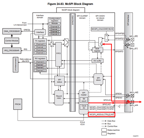
    While further reviewing the register configuration, we examined the McSPI Block Diagram and came to a plausible inference:

    We believe the reason McSPI is not functioning correctly under this configuration is as follows.
    Referencing the McSPI Block Diagram, it shows that the Shift Register uses an internal clock when transmitting data.
    However, for receiving data, the clock source comes from the SCLK pin input.

    This suggests that the SCLK pin is not controlled by the DPE0/DPE1 (data line selection) settings.
    Instead, its direction (input/output) is determined by the MS (Master/Slave) bit field in the Module Control Register.
    As a result, it is possible to configure the SCLK pin to allow both input and output (e.g., pad configured as input, MS bit set for master mode to output SCLK).

    In this configuration, the SCLK signal output from the SPI master can be immediately looped back into the input buffer and used as the receive clock for the RX buffer.

    Consequently, we found that all other settings could remain as before, and enabling just the Receive Enable bit field in CTRL_CORE_PAD_SPI1_SCK was sufficient to make the SPI communication function correctly.

    Thank you.

  • Hi DaeWon,

    Thank you for the detailed explanation. Is any further support required on this issue? If not, could you please close the thread?

    Regards,

    Karthik