

Other Parts Discussed in Thread: TMUXHS4412, TPS65950, AM62L, TDA4VH, TDA4VM, SYSCONFIG, DRA829, EVMK2GX, TIDEP-0100
Tool/software:
Hi TI experts,
Please share links for Standard layout practices or Board Layout recommendations

Tool/software:
Hi TI experts,
Please share links for Standard layout practices or Board Layout recommendations
Hi Board designers.
Please refer below for Standard layout practices and Board Layout Guidelines:
High-Speed Interface Layout Guidelines
https://www.ti.com/lit/pdf/spraar7
Jacinto7 AM6x, TDA4x, and DRA8x High-Speed Interface Design Guidelines
https://www.ti.com/lit/pdf/spracp4
https://www.ti.com/lit/pdf/SPRAC76
AM62x, AM62Lx DDR Board Design and Layout Guidelines
https://www.ti.com/lit/an/sprad06c/sprad06c.pdf
AM62Ax, AM62Px, AM62Dx LPDDR4 Board Design and Layout Guidelines
https://www.ti.com/lit/pdf/sprad66
Jacinto7 AM6x/TDA4x/DRA8x LPDDR4 Design Guidelines
https://www.ti.com/lit/pdf/spracn9
High-Speed Layout Guidelines
https://www.ti.com/lit/pdf/scaa082
High Speed PCB Layout Techniques
https://www.ti.com/lit/pdf/slyp173
High-Speed Layout Guidelines for Signal Conditioners and USB Hubs
https://www.ti.com/lit/pdf/slla414
High-Speed PCB Layout for PCIe
https://www.ti.com/lit/pdf/snla426
https://www.ti.com/video/6287846626001
Layout Guidelines of PCIe® Gen 4.0 Application With the TMUXHS4412 Multiplexer
https://www.ti.com/lit/pdf/slaae45
PCB Design Guidelines For Reduced EMI
https://www.ti.com/lit/pdf/szza009
Understanding TI’s PCB Routing Rule-Based DDR Timing Specification
https://www.ti.com/lit/pdf/spraav0
General High Speed Layout Guidelines
https://www.ti.com/lit/pdf/sllu149
LVDS
https://www.ti.com/video/5966407187001
https://www.ti.com/video/6195144570001
High Speed Clock Distribution Design Techniques for CDC 509/516/2509/2510/2516
https://www.ti.com/lit/pdf/slma003
TPS65950 Layout Guide
https://www.ti.com/lit/pdf/swcu055
Useful links
The FAQ is being updates.
Please review the FAQ frequently for updates.
Regards,
Sreenivasa

Hi Board designers.
Please refer below E2E links:
(+) SK-AM62A-LP: Board layout - Processors forum - Processors - TI E2E support forums
The timing characteristics are provided in the datasheet.
Recommendation is to follow general high speed routing guidelines.
Additionally for relevant peripherals, trace length and matching requirements are defined in the respective Timing Conditions table found in the timing sections of the datasheet.
There is no relationship between CK and Data groups, so it is not necessary to maintain any length differences.
(+) SK-AM62: LPDDR4 HDI Layout guideline - Processors forum - Processors - TI E2E support forums
We do not require VTT termination for point to point designs with only one DDR4 device. This is what the AM62x SK EVM demonstrates
Maybe they are they looking for package delays? This is in the DDR layout guidelines: https://www.ti.com/lit/pdf/sprad06 in section 5
What the customer wants to know is below parameters.
a) CMD/ADD/CTRL signal delay(min/max) against CLK signal
b) DQS signal delay(min/max) against CLK signal
c) DQ signal delay(min/max) against DQS signal
The background of the question is;
The customer thinks total delay consist of (delay of PCB) + (package delay) + (above parameters a/b/c)
The signal delays are optimized during training and will most likely be different with every initialization cycle. The hardware training algorithms will adjust the relative skews of the signals for optimal timing. As long as you provide the correct DDR configuration using the DDR Register Configuration tool, https://dev.ti.com/sysconfig/?product=Processor_DDR_Config&device=AM62x, the controller/PHY training procedure will generate optimal skews across the signals in question. Signal delay values that are applied as calculated during training are only available as encoded values and do not represent anything the customer can use.
Note that if you only have one DDR4 device with only one load on the addr/ctrl signals, then VTT termination is not required (an update to the app note to reflect this is pending). Thus you wouldn't need to worry about AT length.
The document states that when using a single DDR4 chip, VTT termination is optional. So, could you please explain what the differences are between having VTT and not having it, and whether this has any impact on the performance of DDR? Would there be any potential problems if the VTT connector is not designed?
VTT termination is mainly for signal integrity, it does not affect functional performance of DDR in regards to bandwidth or latency. If you're meaningfully concerned about signal integrity for your board, you should follow the document you referenced (DDR layout guidelines for AM62L https://www.ti.com/lit/pdf/sprad06) and consider performing board level simulations to verify signal integrity. You can also reach out to the memory vendor of your DRAM to seek additional recommendations as well.
But I also like to know if the pin package delay can be ignored without issues?
Also, should the pin package delay of the DDR chip in use be considered as well?
Pin package delay consideration should not be necessary. During the training process, there is per-bit deskew which can compensate for package length mismatches. As long as you match pin to pin on board according to the skews in the appnote, the training will take care of optimizing skews across byte lanes and ctrl/addr signals
The document states that when using a single DDR4 chip, VTT termination is optional. So, could you please explain what the differences are between having VTT and not having it, and whether this has any impact on the performance of DDR? Would there be any potential problems if the VTT connector is not designed?
VTT termination is mainly for signal integrity, it does not affect functional performance of DDR in regards to bandwidth or latency. If you're meaningfully concerned about signal integrity for your board, you should follow the document you referenced (DDR layout guidelines for AM62L https://www.ti.com/lit/pdf/sprad06) and consider performing board level simulations to verify signal integrity. You can also reach out to the memory vendor of your DRAM to seek additional recommendations as well.
(+) AM6412: Layout Review of AM6412 and DDR - Processors forum - Processors - TI E2E support forums
No, sorry, we don't get into layout reviews or simulations with customers. We can do a schematic review if needed. Please refer to the following for layout guidelines: https://www.ti.com/lit/pdf/sprad06
For simulation, you can check section 3 of this app note. Although it is for a different device, a lot of the information in section 3 will apply to AM62x: https://www.ti.com/lit/pdf/sprad66
increasing trace impedances to 50/100 should be ok, there may be some adjustment that need to be made to the drive strength or termination values, but those are software configurable. Board SI simulations are encouraged to ensure proper signal integrity and come up with those optimized values. Be sure to follow all the guidelines in AM62x DDR Layout Guidelines app note: https://www.ti.com/lit/pdf/sprad06
(+) DRA821U: LPDDR4 layout simulation - Processors forum - Processors - TI E2E support forums
As mentioned in the application note - the S-param inspection is not pass/fail, but rather a guide to help identify possible issues. The pass fail simulations are the eye diagrams.
MCASP is a standard interface provided on multiple family of TI devices. Please refer below. Only requirement is to add series resistor for the clock and other signals.
https://www.ti.com/lit/an/sprack0/sprack0.pdf
https://www.ti.com/lit/an/sprace0a/sprace0a.pdf
No - we do not have any layout guide for the interfaces mentioned. We have 2 hardware references you can use for guidance: SKAM69 and J784S4XEVM. I also recommend reviewing the Jacinto7 High Speed Guidelines application note (Link). It includes some good general recommendations for PCB routing.
Section 1 of the previously reference document (Jacinto7 High Speed Guidelines) provides general PCB routing recommendations for all high speed signals - including the interfaces you mentioned. Recommendations include impedance control, use of solid GND planes, via suggestions, etc.
VOUT, RGMII, eMMC, and SD interfaces are sourced from LVCMOS drivers. They are recommended to be routed with 50-ohms SE traces. The processor web page includes IBIS models to simulate these interfaces with your PCB to determine any possible signal integrity/coupling issues (dependent on you PCB board materials, via plan, and overall trace lengths)
(+) TDA4VE-Q1: MMC layout guidelines - Processors forum - Processors - TI E2E support forums
The SD and JEDEC industrial specifications provide guidelines on electrical and mechanical connections of the card
and controller for reliable operation. You must follow these guidelines to ensure proper functionality.
TI offers a schematic checklist as well. For more information on the checklist – or to submit your board layout
files for review with TI – approach your local Field Application Engineer to understand the review submission
process.
A few of the recommended signal integrity best practices include:
• Separate routing layers with GND layers.
• Avoid gaps in ground plane between source and load.
• Wherever a signal goes through a via, have a return GND via very close (within a few mm).
• Avoid cross-talk/coupling. Do not route two signals directly above or below each other.
• Avoid cross-talk/coupling. Route traces with spaces between traces that are 2-3X the trace width.
• Avoid stubs. Have zero stubs on traces.
• Ensure signals are monotonic at inputs
• Ensure impedance match
That is my design - "the other pair's" bulge is comming outside of the picture (due to the via's space constraint)
2.) Could I finally repeat if I got you right:
a.) All high speed signals (e.g. PCIe, CSI/DPHY) have no "internal" (within chip package) skew and hence start at the balls with zero skew.
b.) If I want to address TI's recommendations I've to add the length on the pcb as of spraar7i:
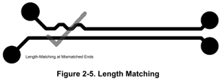
2a) Correct - assume package has zero skew
2b) Correct - minimize impedance discontinuity by adjusting skew mismatches at single/few locations.
https://www.ti.com/lit/an/sprac76g/sprac76g.pdf
High-Speed Interface Layout Guidelines
https://www.ti.com/lit/an/spraar7j/spraar7j.pdf
Jacinto7 AM6x, TDA4x, and DRA8x High-Speed Interface Design Guidelines
https://www.ti.com/lit/an/spracp4a/spracp4a.pdf
AM62Ax, AM62Px, AM62Dx LPDDR4 Board Design and Layout Guidelines
https://www.ti.com/lit/an/sprad66b/sprad66b.pdf
Jacinto7 AM6x/TDA4x/DRA8x LPDDR4 Design Guidelines
https://www.ti.com/lit/an/spracn9f/spracn9f.pdf
(+) TDA4VH-Q1: LPDDR4 layout - Processors forum - Processors - TI E2E support forums
1) The table showing the performance impacts from different PCB stack-ups was originally done from TDA4VM. However - TDA4VH uses same/similar LPDDR4 IP and thus should expect similar results.
2) TI EVMs targeted a slightly lower impedance (33-ohms vs 35-ohms) due to the difficulty achieving the 2x impedance for the T-branches (66-ohms vs 70-ohms). Depending on the specific PCB trace width restrictions, it can be difficult to achieve the higher impedances. The recommendation is to get as close as the design allows (to 2x the base impedance), and the simulations will confirm if it is close enough. Lowering the base impedance lowers the T-branch impedance - allowing the achieved impedance closer to target.
Jacinto 7 High-Speed Interface Layout Guidelines
Then higher impedance is okay.
In lightly loaded signals, such as point-to-point signaling; 50 to 60 ohm single-ended and 80 to 100 ohm differential are common.
Keep in mind tolerance of manufacture may add or subtract 10% to the actual impedance.
It is easier to lower trace impedance by using wider traces than make traces thinner as they sometimes become too thin for manufacture. Dielectric thickness in the stack-up (distance from reference plane) is the other way to change impedance.
Additional inputs
If there are multiple DRAMs and the command/address hit multiple loads, then it may be required to use lower impedance - 35 to 45 ohm single-ended and 70 to 100 ohm differential.
(+) AM6442: DDR Design and Layout Questions - Processors forum - Processors - TI E2E support forums
The requirements are from pin to pin. You do not need to consider the package pin delays, as the training algorithm will compensate for any further mismatch caused by the package
(+) AM6412: DDR4 unused pins - Processors forum - Processors - TI E2E support forums
(+) AM6442: DDR board design - Processors forum - Processors - TI E2E support forums
We typically don't provide that information as the IBIS model should include coupled package RLC parasitics which are far more accurate than delay estimates.
(+) AM4378: AM4378 Layout Guidelines - Processors forum - Processors - TI E2E support forums
DDR layout guidelines are available in the AM437x device datasheet in the TIming and Switching Characteristics section, and RGMII details are available in the High-Speed Interface Layout Guidelines (SPRAAR7). We do not provide any specific layout guides for the other interfaces. Standard layout practices should be followed.
(+) AM5706: Layout to minimize layers - Processors forum - Processors - TI E2E support forums
Hi Brian, you connection looks correct. We have shared address/CKE/CK signals for the two channels, so those signals need to be t-branched on the board to each channel on the memory. The CS signals, however, are point to point. I think this still meets Nanya datasheet statement, as i think the statement is just requiring a separate signal for each channel (ie, you don't need to t-branch the CS signal).
It looks like your device is dual-die, dual channel, single rank. So each channel is in a separate die
What you have designed should be operational. You would need to use the DDR register configuration tool: https://dev.ti.com/sysconfig/?product=Processor_DDR_Config&device=AM62Ax to configure the DDR appropriately.
Based on this configuration, should the customer be configuring 1 or 2 chip selects in Sysconfig? It's a little confusing based off of the terminology shared in the Nanya datasheet, which I can share offline if needed.
it is single rank, so you should configure for 1 chip select
The PCB design is CRITICAL to achieve full data rate of the LPDDR4 interface. Yes - the guidelines provide an example stack-up including which layers to route power and signals. This recommendation is to help improve both signal and power integrity - both of which are critical for LPDDR4. All of the guidelines sections are important - including the simulation section. We strongly recommend 3D simulations be run on PCB design to help ensure successful design.
The data bytes are routed at 40SE and 80DIFF. The clock and control interfaces are routed at lower impedances due to the T-branch portions of the traces.
The recommendation is to double the impedance at the branch location, meaning this requires impedances of 80SE and 160DIFF - likely not supported by your PCB stack-up. For this reason, we recommend your T-branch segments get as close as possible to the desired impedance and then perform simulations to see the impact. For our designs, we lowered the the traces to 33SE and 66DIFF. The T-branch segments targets are now 66SE and 132DIFF. Again - our PCB stackup can reach those targets either, but the difference from target to actual is less using the lower impedances.
(+) TDA4VE-Q1: processor layout design - Processors forum - Processors - TI E2E support forums
The Jacinto7 LPDDR4 Layout Guidelines (link) includes some simulation results for with and without back-drill. Those simulations show that the longer via stubs can impact maximum frequency of interface. There are other mechanism - like board thickness - that can also impact the length of via stubs. Our recommendation is to limit the via stub lengths and back-drilled vias is one approach to doing that.
i would say if they can pass simulations with a certain impedance, then they should use that for silicon. They should still perform memory stress tests across temp to ensure robustness.
Since memories only have one setting for CA/CS, we choose 80ohm. Then since CS is point to point, CS driver is set to 80ohm. Since CA signals are T-branched, CA driver is set to 40ohm, and because of the T-branch, each branch would then be 80ohm. This combination provides the best chance for impedance matching.
(+) AM62P-Q1: PCB material for LPDDR4 usage - Processors forum - Processors - TI E2E support forums
standard PCB material can be used. Please follow the guidelines here: https://www.ti.com/lit/pdf/sprad66
T-branching is required for the CA lines. Please follow the guidelines in the app note. Fly-by topology is not allowed.
Regarding the LPDDR4 connection, see
The [AM62x data sheet] (P1/263) states 4GBytes with LPDDR4, but the [AM62x, AM62Lx DDR Board Design and Layout Guidelines] (P22/44) states Max2GBytes. Which is correct?
[AM62x, AM62Lx DDR Board Design and Layout Guidelines] (P22/44) states that it is possible to connect the Dual specification with Single.
In this case, is it necessary to process the pins of the other memory area of LPDDR4?
it is technically possible to get 4GB of LPDDR4 with AM62x, however, as noted in the Layout guidelines, you would have to use a dual rank, dual channel LPDDR4 and only connect 1 rank to avoid splitting the data bus on the board. Thus, you would not be able to access half of the memory.
So the layout guidelines suggests that if you are needing more than 2GB of memory, you should use DDR4.
When using 4GB(Dual) of LPDDR4, do I need to process unused pins?
you can leave most of the unused pins unconnected. The unused DQS signals on the memory should be pulled to opposite polarity (ie, DQS_t pulled low, DQS_c pulled high) with a 1K resistor
all the VBUS stages (different threshold voltages) are defined in the USB2.0 Specifications
(+) AM3359: Layout guideline - Processors forum - Processors - TI E2E support forums
DDR design guidelines are given in section 7.7.2 of the AM335x Datasheet Rev. J. Other than that there are some general documents that you can refer:
www.ti.com/.../scaa082a.pdf
www.ti.com/.../spraar7h.pdf
www.ti.com/.../sprac76c.pdf
There are no specific requirements for AM335x other than these.
(+) AM3358: PCB layout guidelines - Processors forum - Processors - TI E2E support forums
DDR layout guidelines can be found in section 7.7.2.3 of the AM335x Datasheet Rev. K.
For decoupling capacitors please refer to section 5.9. General PDN guidelines are available here: http://www.ti.com/lit/an/sprac76c/sprac76c.pdf
High-speed interface layout guidelines can be found here: http://www.ti.com/lit/an/spraar7h/spraar7h.pdf
Please note that we do not offer PCB layout reviews or SI analysis for Sitara devices.
Have a look at the Hardware Design Gudie for Keystone devices:
www.ti.com/.../sprabv0.pdf
As well as the SerDes Implementation Guide for Keystone ( devices:
www.ti.com/.../sprabc1.pdf
(+) AM5728: PCIe Layout - Processors forum - Processors - TI E2E support forums
There are no special design guidelines for CLKOUT1 layout. You can follow the general guidelines for high-speed layout: www.ti.com/.../scaa082.pdf
Make the trace impedance approximately 50 ohms and use a 22-33 ohm series termination resistor located as close as possible to the AM335x pin. The reflection that returns from the far-end of the non-terminated transmission line will be mostly absorbed by the series termination resistor and source impedance of the output buffer.
Regards,
Sreenivasa
Below are key guidelines for ensuring the safety and reliability of your system.
To implement functional safety with the TI DRA829 SoC, you need to focus on ensuring power and signal integrity, isolating critical systems, and designing fault detection and recovery mechanisms. Each domain (Main Domain and MCU Domain) should be independently designed to ensure that any fault in one domain does not affect the other, and that the system as a whole remains safe even during failures. By following these guidelines, you can build a system that meets functional safety requirements and operates reliably in critical applications.
Hi Board designers.
Please refer additional collaterals for PDN
AM26x Hardware Design Guidelines
https://www.ti.com/lit/ug/sprabj8d/sprabj8d.pdf
PCB Design Requirements for VDD_MPU_IVA Power
Distribution Network for TI OMAP3630, AM37xx, and
DM37xx Microprocessors
https://www.ti.com/lit/an/sprabj7/sprabj7.pdf
66AK2G1x: EVMK2GX General Purpose EVM Power
Distribution Network Analysis
https://www.ti.com/lit/an/sprace6/sprace6.pdf
How to Measure Impedance of a Power Distribution
Network of a DC-DC Converter
https://www.ti.com/lit/an/sluaai3/sluaai3.pdf
Power Delivery Network Analysis
www.ti.com/.../swpa222a.pdf
66AK2G0x General-Purpose EVM Power Distribution
Network Analysis
www.ti.com/.../sprac38.pdf
TI Designs: TIDEP-0100
AM570x Six-Layer Reference Design
www.ti.com/.../tidue41.pdf
General hardware design/BGA PCB design/BGA
decoupling
www.ti.com/.../sprabv2.pdf
Regards,
Sreenivasa