AM620-Q1: SPL is working but SBL is failing

Part Number: AM620-Q1
Other Parts Discussed in Thread: AM625

Tool/software:

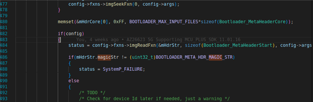
I have seen a weird behavior where my spl is working with its lpddr configuration but it is failing when I use the same for sbl why does this happen .If i do put logs and check it fails here differently at here ...

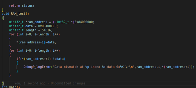
Then i proceeded to do some ram test where i do some write and read similarly like 0xDEADBEEF to offsets and read it back it fails can you explain me why this might be happening  ?


SYSFW Firmware Version 11.1.2--v11.01.02 (Fancy Rat)
SYSFW Firmware revision 0xb
SYSFW ABI revision 4.0

Performing ram test
ERROR: RAM_test:275: Data mismatch at 84000000 index 0 data 0x0
ERROR: RAM_test:275: Data mismatch at 84000004 index 1 data 0x0
ERROR: RAM_test:275: Data mismatch at 84000008 index 2 data 0xBE000000
ERROR: RAM_test:275: Data mismatch at 8400000C index 3 data 0xFEEFFEEF
ERROR: RAM_test:275: Data mismatch at 84000010 index 4 data 0xFE00FE00
ERROR: RAM_test:275: Data mismatch at 84000014 index 5 data 0xFE00FE00
ERROR: RAM_test:275: Data mismatch at 84000018 index 6 data 0xFEEFFEEF
ERROR: RAM_test:275: Data mismatch at 8400001C index 7 data 0xFE00FE00
ERROR: RAM_test:275: Data mismatch at 84000020 index 8 data 0x0
ERROR: RAM_test:275: Data mismatch at 84000024 index 9 data 0x0
ERROR: RAM_test:275: Data mismatch at 84000028 index 10 data 0xBE000000
ERROR: RAM_test:275: Data mismatch at 8400002C index 11 data 0xFEEFFEEF
ERROR: RAM_test:275: Data mismatch at 84000030 index 12 data 0xFE00FE00
ERROR: RAM_test:275: Data mismatch at 84000034 index 13 data 0xFEEFFEEF
ERROR: RAM_test:275: Data mismatch at 84000038 index 14 data 0xFEEFFEEF
ERROR: RAM_test:275: Data mismatch at 8400003C index 15 data 0xFEEFFEFF
ERROR: RAM_test:275: Data mismatch at 84000040 index 16 data 0x0
ERROR: RAM_test:275: Data mismatch at 84000044 index 17 data 0xDEADDEAC
ERROR: RAM_test:275: Data mismatch at 84000048 index 18 data 0xBEEF0000
ERROR: RAM_test:275: Data mismatch at 8400004C index 19 data 0xFEEFFEEF
ERROR: RAM_test:275: Data mismatch at 84000050 index 20 data 0xFEEFFEEF
ERROR: RAM_test:275: Data mismatch at 84000054 index 21 data 0xFEEFFEEF
ERROR: RAM_test:275: Data mismatch at 84000058 index 22 data 0xFEEFFEEF
ERROR: RAM_test:275: Data mismatch at 8400005C index 23 data 0xFEEFFEEF
ERROR: RAM_test:275: Data mismatch at 84000060 index 24 data 0x0
ERROR: RAM_test:275: Data mismatch at 84000064 index 25 data 0xBEEF0000
ERROR: RAM_test:275: Data mismatch at 84000068 index 26 data 0xFEEFFEEF
ERROR: RAM_test:275: Data mismatch at 8400006C index 27 data 0xFEEFFEEF
ERROR: RAM_test:275: Data mismatch at 84000070 index 28 data 0xFEEFFEEF
ERROR: RAM_test:275: Data mismatch at 84000074 index 29 data 0xFEEFFEEF
ERROR: RAM_test:275: Data mismatch at 84000078 index 30 data 0xFEEFFEEF
ERROR: RAM_test:275: Data mismatch at 8400007C index 31 data 0xFEEFFEEF
ERROR: RAM_test:275: Data mismatch at 84000080 index 32 data 0x0
ERROR: RAM_test:275: Data mismatch at 84000084 index 33 data 0xDEADDEAC
ERROR: RAM_test:275: Data mismatch at 84000088 index 34 data 0xBEEF0000
ERROR: RAM_test:275: Data mismatch at 8400008C index 35 data 0xFEEFFEEF
ERROR: RAM_test:275: Data mismatch at 84000090 index 36 data 0xFEEFFEEF
ERROR: RAM_test:275: Data mismatch at 84000094 index 37 data 0xFEEFFEEF
ERROR: RAM_test:275: Data mismatch at 84000098 index 38 data 0xFEEFFEEF
ERROR: RAM_test:275: Data mismatch at 8400009C index 39 data 0xFEEFFEEF
ERROR: RAM_test:275: Data mismatch at 840000A0 index 40 data 0x0
ERROR: RAM_test:275: Data mismatch at 840000A4 index 41 data 0x0
ERROR: RAM_test:275: Data mismatch at 840000A8 index 42 data 0xBEEF0000
ERROR: RAM_test:275: Data mismatch at 840000AC index 43 data 0xFEEFFEEF
ERROR: RAM_test:275: Data mismatch at 840000B0 index 44 data 0xFEEFFEEF

  • Hi Sai,

    I am assigning this to the concerned expert, please wait for their response.

    Best Regards,

    Meet.

  • Hi,

    i do some write and read similarly like 0xDEADBEEF to offsets and read it back

    Are these CPU writes and CPU reads?

    Or OSPI peripheral is involved? (low chance of this being true)

    If yes, then please check in order:

    1.  [FAQ] [AM6XX]: How to check if device type is HS-SE, HS-FS or GP? 
    2. Use the right images accordingly.
    3. If the region you are writing to/reading from is Cached, then make sure to have cache operations like writeback and invalidate before and after the transaction.

    Best,

    Vaibhav

  • this is the sbl_ospi_linux_stage1 and 2 I am using ospi and the ram test I did was something like the image below in the sbl_ospi_linux_stage1 's main.c.

    I was using hs-fs images for SPL boot and the devices are hs-fs 


    if I remove my ram_test code this is the error 

    SYSFW Firmware Version 11.1.2--v11.01.02 (Fancy Rat)
    SYSFW Firmware revision 0xb
    SYSFW ABI revision 4.0


    Some tests have failed!!

    And I am not using cached enable option here is my syscfg configuration for your reference 

    /**
    * These arguments were used when this file was generated. They will be automatically applied on subsequent loads
    * via the GUI or CLI. Run CLI with '--help' for additional information on how to override these arguments.
    * @cliArgs --device "AM62x" --part "Default" --package "ALW" --context "r5fss0-0" --product "MCU_PLUS_SDK_AM62x@11.00.00"
    * @v2CliArgs --device "AM625" --package "FCBGA (ALW)" --variant "AM6254-G" --context "r5fss0-0" --product "MCU_PLUS_SDK_AM62x@11.00.00"
    * @versions {"tool":"1.23.0+4000"}
    */

    /**
    * Import the modules used in this configuration.
    */
    const flash = scripting.addModule("/board/flash/flash", {}, false);
    const flash1 = flash.addInstance();
    const bootloader = scripting.addModule("/drivers/bootloader/bootloader", {}, false);
    const bootloader1 = bootloader.addInstance();
    const bootloader2 = bootloader.addInstance();
    const ddr = scripting.addModule("/drivers/ddr/ddr", {}, false);
    const ddr1 = ddr.addInstance();
    const gtc = scripting.addModule("/drivers/gtc/gtc");
    const mcu_bist = scripting.addModule("/drivers/mcu_bist/mcu_bist", {}, false);
    const mcu_bist1 = mcu_bist.addInstance();
    const qos = scripting.addModule("/drivers/qos/qos", {}, false);
    const qos1 = qos.addInstance();
    const clock = scripting.addModule("/kernel/dpl/clock");
    const debug_log = scripting.addModule("/kernel/dpl/debug_log");
    const mpu_armv7 = scripting.addModule("/kernel/dpl/mpu_armv7", {}, false);
    const mpu_armv71 = mpu_armv7.addInstance();
    const mpu_armv72 = mpu_armv7.addInstance();
    const mpu_armv73 = mpu_armv7.addInstance();
    const mpu_armv74 = mpu_armv7.addInstance();
    const mpu_armv75 = mpu_armv7.addInstance();
    const mpu_armv76 = mpu_armv7.addInstance();
    const mpu_armv77 = mpu_armv7.addInstance();
    const mpu_armv78 = mpu_armv7.addInstance();
    const mpu_armv79 = mpu_armv7.addInstance();
    const mpu_armv710 = mpu_armv7.addInstance();
    const mpu_armv711 = mpu_armv7.addInstance();

    /**
    * Write custom configuration values to the imported modules.
    */
    bootloader1.EMMCAppImageOffset = "0x800000";
    bootloader1.$name = "CONFIG_BOOTLOADER_FLASH_MCU";
    bootloader1.appImageOffset = "0x100000";

    bootloader2.EMMCAppImageOffset = "0xC00000";
    bootloader2.$name = "CONFIG_BOOTLOADER_FLASH_SBL";
    bootloader2.appImageOffset = "0x80000";

    flash1.$name = "CONFIG_FLASH0";
    bootloader1.flashDriver = flash1;
    bootloader2.flashDriver = flash1;
    flash1.serialFlashDriver.$name = "board_flash_serialFlash_serialflash0";
    flash1.serialFlashDriver.fname = "W25Q128JVFAM";
    flash1.serialFlashDriver.protocol = "1s_1s_4s";
    flash1.serialFlashDriver.flashSize = 16777216;
    flash1.serialFlashDriver.flashDeviceId = "0x4018";
    flash1.serialFlashDriver.flashBlockSize = 65536;
    flash1.serialFlashDriver.cmdBlockErase3B = "0xD8";
    flash1.serialFlashDriver.cmdBlockErase4B = "0x00";
    flash1.serialFlashDriver.cmdSectorErase3B = "0x20";
    flash1.serialFlashDriver.cmdSectorErase4B = "0x00";
    flash1.serialFlashDriver.cmdRd = "0x6B";
    flash1.serialFlashDriver.cmdWr = "0x32";
    flash1.serialFlashDriver.dummyClksRd = 8;
    flash1.serialFlashDriver.proto_isAddrReg = false;
    flash1.serialFlashDriver.proto_cmdRegRd = "0x00";
    flash1.serialFlashDriver.proto_cmdRegWr = "0x00";
    flash1.serialFlashDriver.proto_mask = "0x00";
    flash1.serialFlashDriver.proto_bitP = 0;
    flash1.serialFlashDriver.dummy_isAddrReg = false;
    flash1.serialFlashDriver.dummy_cmdRegRd = "0x00";
    flash1.serialFlashDriver.dummy_cmdRegWr = "0x00";
    flash1.serialFlashDriver.enable4BAddr = false;
    flash1.serialFlashDriver.xspiWipRdCmd = "0x05";
    flash1.serialFlashDriver.flashManfId = "0xEF";
    flash1.serialFlashDriver.peripheralDriver.$name = "CONFIG_OSPI0";
    flash1.serialFlashDriver.peripheralDriver.dmaEnable = true;
    flash1.serialFlashDriver.peripheralDriver.OSPI.D7.rx = false;
    flash1.serialFlashDriver.peripheralDriver.OSPI.D6.rx = false;
    flash1.serialFlashDriver.peripheralDriver.OSPI.D5.rx = false;
    flash1.serialFlashDriver.peripheralDriver.OSPI.D4.rx = false;

    ddr1.$name = "CONFIG_DDR0";
    ddr1.ddrConfigIncludeFileName = "drivers/ddr/v0/soc/am62x/board_lpddrReginit.h";

    mcu_bist1.$name = "CONFIG_MCU_BIST0";

    qos1.$name = "CONFIG_QOS0";

    const udma = scripting.addModule("/drivers/udma/udma", {}, false);
    const udma1 = udma.addInstance({}, false);
    udma1.$name = "CONFIG_UDMA0";
    flash1.serialFlashDriver.peripheralDriver.udmaDriver = udma1;
    bootloader1.udmaDriver = udma1;
    bootloader2.udmaDriver = udma1;

    const udma_blkcopy_channel = scripting.addModule("/drivers/udma/udma_blkcopy_channel", {}, false);
    const udma_blkcopy_channel1 = udma_blkcopy_channel.addInstance({}, false);
    udma_blkcopy_channel1.$name = "CONFIG_UDMA_BLKCOPY_CH0";
    flash1.serialFlashDriver.peripheralDriver.udmaBlkCopyChannel = udma_blkcopy_channel1;
    bootloader1.udmaBlkCopyChannel = udma_blkcopy_channel1;
    bootloader2.udmaBlkCopyChannel = udma_blkcopy_channel1;

    clock.instance = "TIMER1";

    debug_log.enableUartLog = true;
    debug_log.enableCssLog = false;
    debug_log.sysfwUartTrace = true;
    debug_log.uartLog.$name = "CONFIG_UART0";
    debug_log.uartLog.intrEnable = "DISABLE";
    debug_log.uartLog.useWakeupDomainPeripherals = false;
    debug_log.sysfwUartLog.$name = "CONFIG_UART_TRACE0";
    debug_log.sysfwUartLog.useWakeupDomainPeripherals = false;
    debug_log.sysfwUartLog.UART.$assign = "USART1";
    debug_log.sysfwUartLog.UART.RXD.$assign = "MCASP0_AFSR";
    debug_log.sysfwUartLog.UART.TXD.$assign = "MCASP0_ACLKR";
    debug_log.sysfwUartLog.UART.RTSn.$assign = "MCASP0_AXR2";
    debug_log.sysfwUartLog.UART.CTSn.$assign = "MCASP0_AXR3";

    mpu_armv71.$name = "CONFIG_MPU_REGION0";
    mpu_armv71.accessPermissions = "Supervisor RD+WR, User RD";
    mpu_armv71.allowExecute = false;
    mpu_armv71.attributes = "NonCached";

    mpu_armv72.$name = "CONFIG_MPU_REGION1";
    mpu_armv72.accessPermissions = "Supervisor RD+WR, User RD";
    mpu_armv72.size = 7;

    mpu_armv73.$name = "CONFIG_MPU_REGION2";
    mpu_armv73.accessPermissions = "Supervisor RD+WR, User RD";
    mpu_armv73.baseAddr = 0x41C00000;
    mpu_armv73.size = 19;

    mpu_armv74.$name = "CONFIG_MPU_REGION3";
    mpu_armv74.accessPermissions = "Supervisor RD+WR, User RD";
    mpu_armv74.baseAddr = 0x70000000;
    mpu_armv74.size = 16;

    mpu_armv75.$name = "CONFIG_MPU_REGION4";
    mpu_armv75.baseAddr = 0x80000000;
    mpu_armv75.size = 31;

    mpu_armv76.$name = "CONFIG_MPU_REGION5";
    mpu_armv76.baseAddr = 0x41010000;
    mpu_armv76.size = 15;
    mpu_armv76.attributes = "NonCached";

    mpu_armv77.$name = "CONFIG_MPU_REGION6";
    mpu_armv77.size = 15;
    mpu_armv77.attributes = "NonCached";

    mpu_armv78.$name = "CONFIG_MPU_REGION8";
    mpu_armv78.baseAddr = 0x43C00000;
    mpu_armv78.size = 18;

    mpu_armv79.$name = "CONFIG_MPU_REGION7";
    mpu_armv79.baseAddr = 0xFC40000;
    mpu_armv79.size = 8;
    mpu_armv79.attributes = "Device";
    mpu_armv79.allowExecute = false;

    mpu_armv710.$name = "CONFIG_MPU_REGION9";
    mpu_armv710.allowExecute = false;
    mpu_armv710.size = 9;
    mpu_armv710.attributes = "Device";
    mpu_armv710.baseAddr = 0x2800000;

    mpu_armv711.$name = "FSS0_DAT_REG1";
    mpu_armv711.baseAddr = 0x60000000;
    mpu_armv711.size = 27;
    mpu_armv711.attributes = "Device";
    mpu_armv711.allowExecute = false;

    /**
    * Pinmux solution for unlocked pins/peripherals. This ensures that minor changes to the automatic solver in a future
    * version of the tool will not impact the pinmux you originally saw. These lines can be completely deleted in order to
    * re-solve from scratch.
    */
    flash1.serialFlashDriver.peripheralDriver.OSPI.$suggestSolution = "OSPI0";
    flash1.serialFlashDriver.peripheralDriver.OSPI.CLK.$suggestSolution = "OSPI0_CLK";
    flash1.serialFlashDriver.peripheralDriver.OSPI.CSn0.$suggestSolution = "OSPI0_CSn0";
    flash1.serialFlashDriver.peripheralDriver.OSPI.DQS.$suggestSolution = "OSPI0_DQS";
    flash1.serialFlashDriver.peripheralDriver.OSPI.D7.$suggestSolution = "OSPI0_D7";
    flash1.serialFlashDriver.peripheralDriver.OSPI.D6.$suggestSolution = "OSPI0_D6";
    flash1.serialFlashDriver.peripheralDriver.OSPI.D5.$suggestSolution = "OSPI0_D5";
    flash1.serialFlashDriver.peripheralDriver.OSPI.D4.$suggestSolution = "OSPI0_D4";
    flash1.serialFlashDriver.peripheralDriver.OSPI.D3.$suggestSolution = "OSPI0_D3";
    flash1.serialFlashDriver.peripheralDriver.OSPI.D2.$suggestSolution = "OSPI0_D2";
    flash1.serialFlashDriver.peripheralDriver.OSPI.D1.$suggestSolution = "OSPI0_D1";
    flash1.serialFlashDriver.peripheralDriver.OSPI.D0.$suggestSolution = "OSPI0_D0";
    debug_log.uartLog.UART.$suggestSolution = "USART0";
    debug_log.uartLog.UART.RXD.$suggestSolution = "UART0_RXD";
    debug_log.uartLog.UART.TXD.$suggestSolution = "UART0_TXD";

  • Hi,

    Please refer this FAQ to determine the exact point of failure, instead of adding RAM test.

    FAQ:  [FAQ] AM62X/AM64X : [FAQ] Debugging SBL boot in RTOS SDK 

    Let me know the point after debugging inside wherever the failure occurs, a call stack would help along with a note on if the failure happens in stage 1 or stage 2.

    Looking forward to your response.

    Thanks,

    Vaibhav