This thread has been locked.

If you have a related question, please click the "Ask a related question" button in the top right corner. The newly created question will be automatically linked to this question.

AM69: What happens if I unconnect PWR to specific VDDA_ inputs such as CSI, DSI, MMC0, DDR1,2,3?

Part Number: AM69

Tool/software:

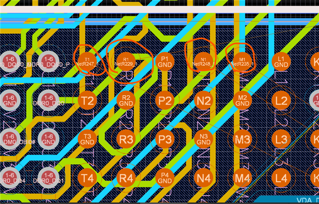
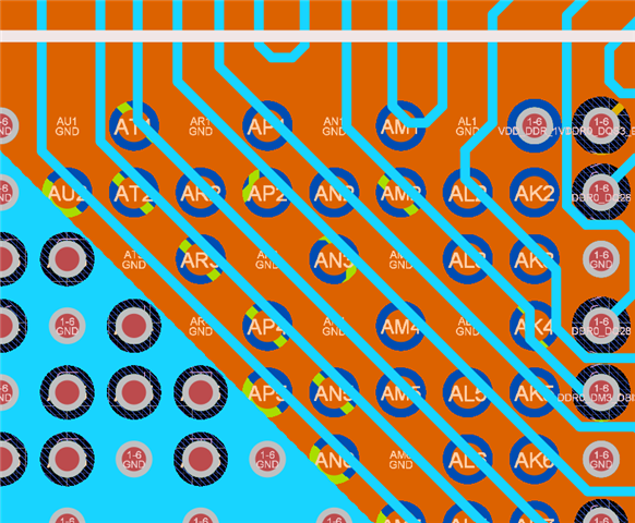
I'm in need to connect certain pads to VSS/GND to make a complete solid reference plane at the top because second layer is used as high speed signal.

I know that you should not connect certain pads/balls of the processor directly to VSS/GND because it can cause current rush. Therfore, it's recommended to add a pull-down resistor instead to protect the IO.

According to " 5.4 Pin Connectivity Requirements" from the datasheet of AM69 processor. There we can find the following:

  • Some pins must be connected directly to an arbitary pull-down to VSS/GND, if unused.
  • Some pins must be connected directly to an approprite pull-down to VSS/GND, if unused.
  • Some pins can be connected directly to VSS/GND, if unused.
  • Some pins must be connected directly to an arbitary pull-up to specific VCC, if unused.

But what if I just remove the power? First of all, I don't need DDR1 to DDR3. Why not remove the 0-ohm resistor that enables the current flow to the processor for DDR1 to DDR3? I only need DDR0.

Same as some of the serdes, all of CSI, DSI and MMC0. I'm only need MMC1 due to the SD-card.

So what would happen if I "unplug" the power to specific peripherals of AM69?

  1. Will the processor still boot?
  2. Will the pins have no voltage? E.g they are like...no connected to anything?
  3. Will it disable the peripheral and no issue will occur?

The reason why I'm asking this question it's because I have not find any information how to disable peripherals at the initial start of the processor. The goal is to connect the whole DDR1 directly to VSS/GND if it's not used.

See the reference schematic SK-AM69 for the PDN.

  • It is required to have all power rails supplied with the correct voltage, even if that function is unused.  For example - VDDA_0P8_USB must be supplied 0.8V even if USB is unused.  I cannot describe what will happen with different combinations of unpowered rails - as TI does not test those unsupported configurations.  The device has no internal protection for the 'partial' power and could potentially damage the device through reverse current paths.

    I don't understand the comment 'goal is to connect the whole DDR1 directly to VSS/GND' comment.  If DDR1 is unused, only need to pull DQS/DQSn signals - other signals can remain open.

  • Thank you so much.

    Well, the reason is that I'm using 6 layer board and I have designed everything with only 6 layers. Including reference plane.

    But the last thing I need to do is to add pull-downs and pull-ups for DDR1 and DDR2. It seems like a easy task, but it's splitting the reference plane. 

  • If IP is not being used, you can also remove the filters.  From previous example I used with VDDA_0P8_USB, you could remove L53, C321, C167, C168 (but still connect VDDA_08_USB to VDD_CORE_0V8.  Maybe that will help reduce the number of separate power rails in BGA area.

  • In this case. The most important thing is DDR1 and DDR2 and MMC0 because they creating holes in the reference plane.

    I don't like that because you should never break or split the reference plane. 

  • A 6Lyr PCB is super aggressive for this device.  If I understand pics, there is no way to avoid issue if any via is connect to BGA pad?  Compromises might need to be made, possibly DDR data rate (void in reference).  CMOS input that are floating can potentially oscillate and damage the device - which is why recommendation to terminate some pins.

  • A 6 layer PCB does not has to be aggresive. Everything counts how well the design is. 

    If I connect e.g DDR_DQS to VSS, then this issue disapears. But connecting them directly to VSS can harm because they are of the type IO. 

    One thing I could do is to remove some balls from the array. But that's too time consuming. 

    Do you think that TI dev team can try to unmount some 0-ohm resistors for the DDR and see what's happens? (on the SK-AM69)?

  • DQS are IO, but do not drive out unless configured to do so.  When booting, the DDR interface is not configured until software configures it.  Thus - if only one interface is configured and the others are disabled, there should be no concern of driving output.  The output is only a concern if you boot software the configures to enable the interface.  The reason for pull-ing up to VDD or VSS is because those IO are not NOT outputs, but inputs only - and may oscillate.  You can connected DQS directly to VSS and DQSn to 1.1V if you guarantee the interfaces are never enabled.

  • What happen if I connect them both to VSS and configure them as inputs?

  • Unknown, but not recommended since its a differential pair and the input is 'clock' when the signals cross. That is reason for strapping them to different voltages.

  • Thank you. I think the "unknown" is the best answer. I think I will try to find it out by doing some experiments.  I will investigate more about configure pins to inputs and tie them to VSS.

  • By the way! Att the directly startup...are the GPIOs randomly selected as inputs and outputs? I was think about connecting the DQS to VSS and 1.1V without the resistor. 

  • If you are referring to DQS and DQSn, these should be inputs by default  If you are referring to GPIO, most default default to mode 7 (which is GPIO mode) and GPIO default as inputs. Below is one example:

    Note ROM code can change these defaults when booting, so if booting XSPI, then ROM will configure the XSPI pins as needed.

  • That means I could tie pads to VSS if they are configured as inputs. Well, the DQS_N must be connected to 1.1V just in case the clock won't oscillate. I will give this a try! Thank you.

  • Most GPIO can be left open (not connected to VSS) because there is an internal pull resistor that can be enabled to keep pin from floating.  See previous response, Pull Type column.  The unused pins that need to be terminated are the pins that don't support internal pull options.

  • Yes I know. But the unused pins that don't offer a internal pull can be pulled directly to VSS without a resistor if the are configured as input only. Well, except analog inputs. They require a specific logic low value. 

  • Ok.  In general terms I will refer you to the unused signals table in the data manual.  It states which should be pull-up or pull-down.  Yes - assuming IO is input (which it should be as that is why it requires a pull resistor), then you can optionally directly connect without resistor.  TI does not recommend that as it does increase risk if that peripheral is enabled.

  • Yes.The peripheral will never be enabled. Thank you. I will make sure that the DDR differential DQS have at least no posibilities to oscillate. I will connect N to 1.1V and P to VSS. All other inputs will be tied to VSS. Except pads that are analog A. I assume they require a specific voltage level to operate. I don't want my processor to fault during boot.