This thread has been locked.

If you have a related question, please click the "Ask a related question" button in the top right corner. The newly created question will be automatically linked to this question.

AM62L: Cannot boot from QSPI flash

Part Number: AM62L
Other Parts Discussed in Thread: TMDS62LEVM, UNIFLASH

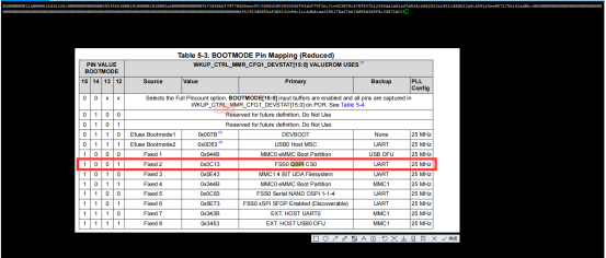
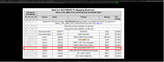
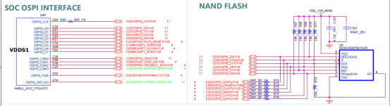
Hello, expert. Currently, we are testing the QSPI FLASH boot of AM62L32. The following is our schematic design

image.png

Whether we use FSS0 QSPI CS0 or FSS0 Serial NAND OSPI 1-1-4 mode, we cannot boot normally. The specific log is as follows; But it can read and write QSPI FLASH normally. May I ask what the reason is?

image.png

image.png


  • Hi Junzhi Lin,

    Thank you for your query !

    Could you please re-upload the schematic diagrams and log screenshot with a better resolution ? I am not able to distinguish the signals / components names and log text in the images.

    Let us also know how are the bootmode pins: 0 through 11 configured ?

    Thanks

    Best Regards,

    Anastas Yordanov

  • Currently, when we use the Reduced Pincount BOOT SET mode and configure the boot method as FSS0 QSPI CS0 and FSS0 Serial NAND OSPI 1-1-4 mode, the following log is always printed. Could you please tell me what the reason is?

    The serial port merely printed the following content

    02000000011a0000616d36326c0000000000000048534653000101000001010002a6000000000000fe73d96bbf79f784d9aee9fc5698d1093936556f93abf79f3ec7ce923079c478f837b12296da2a81a2fa024cb9d2423a14511488622a9ca591e5ee057175b142ad0bc40b000000000000000000000000000000000000000000000000000000000000000000000000000000000000000000000000000000000000000000000000e551f63d6055af48613cb94c1cc4d6dcaa2296178a27eb7dd58d3d5f8c34871bCCCCCCCCCCCCCCCCCCCCCCCCCCCCCCCCCCCCCCCCCCCCCCCC

  • Hi Anastas,

    I have written the tiboot3 image to the mtd0 partition and the tipsl image to the mtd1 partition, but it doesn't seem to have any effect.

  • Hello JUNZHI LIN, Yi Wang,

    Currently, when we use the Reduced Pincount BOOT SET mode and configure the boot method as FSS0 QSPI CS0 and FSS0 Serial NAND OSPI 1-1-4 mode, the following log is always printed. Could you please tell me what the reason is?

    The serial port merely printed the following content

    02000000011a0000616d36326c0000000000000048534653000101000001010002a6000000000000fe73d96bbf79f784d9aee9fc5698d1093936556f93abf79f3ec7ce923079c478f837b12296da2a81a2fa024cb9d2423a14511488622a9ca591e5ee057175b142ad0bc40b000000000000000000000000000000000000000000000000000000000000000000000000000000000000000000000000000000000000000000000000e551f63d6055af48613cb94c1cc4d6dcaa2296178a27eb7dd58d3d5f8c34871bCCCCCCCCCCCCCCCCCCCCCCCCCCCCCCCCCCCCCCCCCCCCCCCC

    Printing the hexadecimal sequence + followed by printing 'C' character in approximately 2 sec. intervals indicates that you are currently in UART boot mode. 

    Would you please provide the exact BOOTMODE setting of the AM62L BOOTMODE0-BOOTMODE15 pins on your custom board ?

    It is very likely that you boot in UART backup mode because your primary boot from QSPI flash memory fails for some reason.

    If you chose a non-UART backup boot mode (less likely) with your primary QSPI boot,  then it seems that you have a wrong hardware bootmode configuration. 

     I hope this helps clarify !

    Thanks

    Kind Regards,

    Anastas Yordanov

  • We only used pins 12 to 15 for Reduced Pincount BOOT SET mode and tried configuring them as 0011 and 1001.

  • Hi Yi Wang, JUNZHI LIN,

    Thanks for the update.

    So I understand, based on the AM62L TRM Section Intialization / Subsection BOOTMODE Pin Mapping (Reduced Pincount):

    that in your configuration, the BOOTMODE pins 0 through 11 scanning ignored after POR because of the BOOTMODE15!=0 && BOOTMODE14!=0 for a reduced boomode pincount selection mode.

    The AM62L ROM bootloader captures [BM12:BM15] = 1001:  “Fixed 2” -> FSS0 QSPI CS0 or [BM12:BM15]=0011: “Fixed 5”-> FSS0 Serial NAND OSPI 1-1-4  configuration values as primary boot sources. From the table it is obvious that UART is the backup boot option. This explains why  you see “… CCCCC” print in the console.

    This means the QSPI boot is unsuccessful and the backup UART boot triggered.

    I will try to provide further checkpoints for the  QSPI unsuccessful boot analysis.  Please expect a response tomorrow.

    Kind Regards,

    Thanks

    Anastas Yordanov

  • Hi Yi Wang, JUNZHI LIN,

    you may want to check the OSPI/QSPI interface related sections of  this FAQ on board bring-up:

    FAQ - Board bring-up

    Let me know what is the state of the checked signals ?

    Thank you

    Kind Regards,

    Anastas Yordanov

  • Hi,

    We can observe from the oscilloscope that after power-on, there is a clock signal on OSPI0_CLK along with a chip select signal on OSPI0_CSN0, but then the system switches to serial port boot, as indicated by the CCC printout.

  • Hi Yi Wang,

    I am not sure where does the pin(9): EP comes from ? Isn't GD5F2GM7REYIGR a 8-pin package ?

    Did the hardware implementation of the OSPI0 host controller QSPI HW interface follow the TI recommendations for hardware design and schematic review checklist (refer the checkpoints in the OSPI/QSPI related sections):

    Hardware design recommendation for custom board design

    AM62L Schematic Design and Schematic Review Checklist

    It seems the AM62L LBCLK0, DQS, CSn1,CSn2,CSn3 are unused for OSPI interface but for other peripheral purposes (i.e. GPIO). Can you confirm ? 

    Here is a very informative FAQ on the OSPI/QSPI topic:

    OSPI/QSPI memory interface

    In the QSPI mode, the loading of the SPL boot software from the QSPI to the RAM will be performed at OSPI0_CLK freq. = 50 MHz in 1S-1S-4S mode. Execution of the boot code is performed from RAM.

    According to the Section Initialization / Subsection, QSPI Boot of the AM62L TRM:

    Regarding QSPI boot interface hardware example you may wish to check the following E2E thread:

    E2E example thread: QSPI boot

    Please expect a follow up with more hints in a day or two.

    Kind Regards

    Anastas Yordanov

  • The pin (9) of GD5F2GM7REYIGR is a heat dissipation ground pad. It is recommended that you do not need to pay attention to it.

  • Hi JUNZHI LIN,

    thanks for your confirmation regarding the power dissipation pad.

    Would it be a problem to provide an oscilloscope image of the OSPI0_CSn0 and OSPI0_CLK, OSPI0_DQ0 at the OSPI NAND memory side during the booting phase ?

    Thanks

    Kind Regards,

    Anastas Yordanov

  • Hi ,

    The following images show the captured waveforms of CLK, CSn0, D0, and D1 during the BOOT phase.There is no data on D2 and D3 during the BOOT phase.

    CLK and CSn0

    CLK and D0

    CLK and D1

    CSn0 and D0

    CSn0 and D1

  • Hi ,

    We conducted tests using the TMDS62LEVM board. The NAND FLASH supports normal read and write operations, but the board still fails to boot.
    Since the CSn0 of TMDS62LEVM is connected to the NOR FLASH, we made the following modifications:

    Removed resistors R477, R465, and chip U100

    Shorted the OSPI_NOR_INTn signal to GND

    Shorted the CSn0 pin of NOR FLASH and the CSn3 pin of NAND FLASH

    The attempted Reduced Pincount configuration is: FSS0 Serial NAND OSPI 1-1-4
    The Full Pincount configuration is as follows:
    BOOTMODE[2:0]: 011
    BOOTMODE[9:3]: 0 0 1 0000
    BOOTMODE[13:10]: 0 0 1 1  or 1 1 0 1
    BOOTMODE[14:15]: 0 0

    If the Backup Mode is UART, it will print the following content;

    if the Backup Mode is SD Card, it will print the following content.

  • Just reminding: I was told GD QSPI NAND flash is in 1s-1s-1s mode other than 1s-1s-4s mode in default  Please take a check. and try 

    BOOTMODE[9:3]: 0 1 x 0000 

  • Hi 
    Following your suggestion, I changed BOOTMODE PIN[8] to 1, but it still fails to boot.

  • Hi junji wu,

    Let me first comment on your setup on the TI TMDS62LEVM board.

    Shorted the OSPI_NOR_INTn signal to GND

    - This means the AM62L EVM GPIO0_13 input is currently shorted to GND. This means the OSPI_NOR_INTn line will permanently trigger IRQ at the AM62L GPIO0_13 input. I am not sure if ROM bootloader processes this IRQ, but to be on the safe side why don't you leave it as it is - only with the pull-up resistor. Thus the IRQ line from the unused NOR Flash will be hold inactive. Please remove connection to GND.

    Please expect a follow-up answer !

    Thanks

    Kind Regards,

    Anastas

  • Hi Tony,

    Thanks for the good hint during the boot analysis. 

    Kind Regards,

    Anastas 

  • Hi ,

    I apologize for the incorrect description of the board modifications. Please refer to the image I provided — actually, I shorted the OSPI_NOR_RSTn pin to GND to prevent the NOR FLASH from interfering with the NAND FLASH boot without removing the NOR FLASH. No modifications were made to the OSPI_NOR_INTn pin.

  • Hi Junji Wu,

    Thanks for answering my question wrt your rework of the TI TMDS62LEVM:

    Regarding your setup on the  TI TMDS62LEVM: 

    Can you show me boot oscillograms of  the NAND Memory clock input QSPI_NAND_CLK, probing as close as possible to the Winbond NAND memory component. This measurement is interesting because the clock is sourced from the AM62L OSPI0_LBCLKO output which behavior depends on the mode (TAP or PHY) to which ROM bootloader sets the OSPI host controller.

    The same measurement regarding the QSPI_NAND_CSn signal. Interesting - because it is tied off to the OSPI0_CSN0 together with the OSPI_NOR_CSn. So it is good to see if there is some impact on the signal shape.

    Can you check the QSPI_NAND_RSTn to see if the QSPI NAND Flash is held in Reset during booting.  

    Is it possible to modify your software to use the OSPI controller OSPI0_CSN3 output for chip select to the EVM Winbond NAND (instead to share the OSPI0_CSN0 with the NOR flash) as per the original EVM. Let me know ?

    Regarding the hint from Tony, would you please verify once again on your custom board that the complete config. of your BOOTMODE settings (Serial NAND primary boot mode + UART backup boot mode) are as follows:

    B15.............................B0

    00_0011_01x0000_011

    Thank you

    Kind Regards,

    Anastas Yordanov

  • Hi ,

    I tested the QSPI_NAND_CLK signal and found there is no clock signal, as shown in the figure below.
    Subsequently, I noted that the Serial NAND BOOT should uses the OSPI0_CLK pin, so I shorted the QSPI_NAND_CLK and OSPI_NOR_CLK pins and attempted to boot again, but it still did not succeed. The current BOOTSETTING mode I'm using is:[15:0]: 00_0011_01x0000_011
    The simplified circuit diagram after modification is shown in the figure below.
    The following images show the waveforms obtained from testing the modified TMDS62LEVM, and its waveforms are similar to those of our own board.
    QSPI_NAND_CLK and OSPI_DQ0
    QSPI_NAND_CS and OSPI_DQ0
    QSPI_NAND_RSTn and OSPI_DQ0
    Thank you for your suggestion to "use the OSPI controller OSPI0_CSN3 output for chip select to the EVM Winbond NAND." Upon reviewing the latest TRM manual, I note that on page 169, it specifies that only CSn0 supports Serial NAND boot. With this in mind, connecting the NAND FLASH's chip select to CSn3 may not enable booting in theory.
    Additionally, I have double-checked and confirmed that we've updated the BOOTMODE setting on our board to 00_0011_01x0000_011 as suggested by Tony, though the board still fails to boot.
  • Hello Junji Wu,

    Thank you for your suggestion to "use the OSPI controller OSPI0_CSN3 output for chip select to the EVM Winbond NAND." Upon reviewing the latest TRM manual, I note that on page 169, it specifies that only CSn0 supports Serial NAND boot. With this in mind, connecting the NAND FLASH's chip select to CSn3 may not enable booting in theory.

    Sorry for misleading you  and thank you for your TRM crosscheck and correction ! My idea was to rather update SW and avoid any deviations from the EVM schematic but I forgot the fact that the AM62L ROM bootloader SW is able to boot only from a CSn0 connected NAND Flash. 

    After connecting the two memories clock pins, you can remove the unused NOR Flash clock R471 pull-down resistor to reduce the load on the OSPI0 controller clock output. I suppose that you have also detached the W25N01JWTBAG  QSPI_NAND_CLK and QSPI_AND_CS from the SoC OSPI0_LBCLKO and  OSPI0_CSN3.

    I am not sure if direct sharing of the AM62L OSPI0_CSn and OSPI0_CLK between the QSPI_NAND and OSPI_NOR memory corresponding CSn and CLK input pins does not violate any signal integrity rule.

    From the following E2E thread at least it seems that such a rework of the EVM is not tested and not recommended by TI:

    Trying to boot from the W25N01JWTBAG NAND on TMDS62LEVM

    Referring to the provided oscillograms, the DQ0 line and CLK seem a bit noisy with noticeable overshoots near rise and fall transition areas. The undershoots seem smaller. I am not able to qualify the overshoot (maybe about 500mV or more) and undershoot magnitude with the used 1V range. Would you be able to provide a DQ0 signal oscillogram with finer resolution i.e. 500 mV or 100 mV. This may be needed to rule out that data logical level of a serial NAND command or address is possibly misinterpreted at the QSPI NAND Flash data input.

    The command sent to the Flash from the AM62L OSPI seems to be 0x0F C0 -> "Read status register-3".

    In order to understand the boot error I need to see a complete CLK, DQ0 command/ DQ1 data transfer sequence like the one you captured here, but with better time scale and  with added clock and chip select:

    For now in the OSPI 1S-1S-1S boot mode (standard SPI mode) the clock frequency also seem to not meet the expected 50 MHz (20ns) frequency of the OSPI0_CLK clock to the NAND Flash memory during ROM loader booting. Is it also 6.26 MHz when data toggles on the DQ1 line ?

     Please expect my follow-up early next week !

    Thanks

    Kind Regards,

    Anastas Yordanov

  • Hi Anastas Yordanov,

    Regarding your assumption that "I suppose that you have also detached the W25N01JWTBAG QSPI_NAND_CLK and QSPI_NAND_CS from the SoC OSPI0_LBCLKO and OSPI0_CSN3," here is an update:

    Since there is no series resistor between the CLK pin of the NAND FLASH and the OSPI0_LBCLKO pin of the AM62Lx, the only way to disconnect their electrical connection would be to cut the trace on the PCB, which carries significant risk. Therefore, we have not performed this operation, and the same logic applies to the CS signal of the NAND FLASH.

    In summary, for the AM62Lx on the TMDS62LEVM board, CSn0 is currently shorted to CSn3, and OSPI0_CLK is shorted to OSPI0_LBCLKO. Based on my tests, during the BOOT phase, CSn3 and OSPI0_LBCLKO do not actually output any signals, so in theory, they should not interfere with CSn0 and OSPI0_CLK.

    Following your suggestion, I have tested the waveforms of CLK/CSn0/D0 and CLK/CSn0/D1 of the NAND FLASH during the boot phase.

    At the 14th clock cycle, the CLK frequency switches to 50MHz. The waveform of D1 seems to exhibit some anomalies: on occasion, it fails to drop to 0V properly. I am unsure if this affects the NAND BOOT process.

    For reference, I tested the read and write functions of the NAND BOOT after booting via an SD card, and no such abnormal waveforms were observed.

    Detailed waveform images are attached.

  • Hi Junji Wu,

    I can see that the lower the width of the D1 pulses, the more obvious is the issue. The level is not low enough.

    Please expect a follow-up shortly.

    Thanks

    Kind Regards,

    Anastas Yordanov


  • Hello Junji Wu,

    Let's start with OSPI CLK  signal:

    There is a visible dip in the plateau zone of the clock pulses. As already mentioned there is a noticeable negative and positive overshoot exceeding by around 500 mV the GND and VDDS1=1.8V power supply potentials. The transient positive overshoot is 2.34 - 1.8 = 0.54 V > 0.2*VDDS1 = 0.2*1.8 = 0.36V lasting for about 3-4 us that is  approximately 20% of T=20us. The negative overshoot  -0.48 V.

    Is it possible that the dip is due to limitations of the equipment used - i.e. the scope, the probes and measurement setup. Q: What are the max frequency and supported sample rate by your oscilloscope and probes ? Do you use for example ground springs to provide a shorter grounding path during the measurements.

    Regarding OSPI0_D0 - as you already summarized, there is no "floating zero" level observed. In the Serial NAND boot mode this is actually the command / address / write data  line.

    The boot software data, supposed to be downloaded to RAM before the boot, is read over the AM62L OSPI0_D1 input. However with the OSPI0_D1 there is an issue with the floating level of the logic zero. If there is a "short" signal transition HIGH to LOW, typically for 1-3 falling clock edges, the signal in some occasions may NOT drop below Vil_max = 0.35*VDDS1 = 0.63V but  is retained above the AM62L 1P8_LVCMOS buffer Vih_min=  0.65*VDDS1 = 1.17V or reaches a level between Vil_max and Vih_min which may lead to wrong interpretation (as HIGH) at the AM62L OSPI0_D1 input.

    And vice versa, if the NAND memory D1 output changes from LOW to HIGH, typically for 1-3 falling clock edges, the signal may not exceed the 1P8_LVCMOS buffer Vil_max threshold  (0.63V) or  reaches a level between Vil_max =0.63V and Vih_min=1.17V and wrongly interpreted as LOW at the AM62L OSPI_D1 input. So there is an issue.

    Since there is no series resistor between the CLK pin of the NAND FLASH and the OSPI0_LBCLKO pin of the AM62Lx, the only way to disconnect their electrical connection would be to cut the trace on the PCB, which carries significant risk. Therefore, we have not performed this operation, and the same logic applies to the CS signal of the NAND FLASH.

    Ok I understand.  Below is the E18 (OSPI0_LBCLKO) and C23(OSPI0_CSn3)  pins default buffer and muxmode values according to the AM62L Datasheet: 

    As per the default SoC pin configuration and ROM sequence, shorting  the SoC LBCLKO pin (HiZ by default & untouched by ROM for booting in the OSPI Tap operation mode  ) to the SoC OSPI0_CLK pin as well as the SoC OSPI0_CSn3 pin (HiZ by default & untouched by ROM) to the SoC OSPI0_CSn0 pin should do no harm to the SoC and Flash memories.

    Also, as per my understanding from the datasheet of the NOR Flash S28HS512TGABHM013:

    Infineon S28HS512TGABHM013 Datasheet

    When OSPI_NOR_RESET reset is asserted, the S28HS512TGABHM013 data pins are forced to HiZ (disconnected) state. However the RESET# input pin of the NOR Flash shall remain active (asserted LOW) only when CS signal is HIGH. So a question emerges what is the state of the Flash NOR data and other output pins when RESET# is asserted LOW while CS is driven LOW by the AM62L OSPI host. The NOR flash datasheet infers that assertion of the CS to "LOW" when RESET# pin is hold "LOW" is kind of an "illegal" state (though not explicitly highlighted).

    Here is a TI FAQ guidance on how to connect two OSPI memories (in particular the NOR: S28HS512TGABHM013 and the NAND: W25N01JWTBAG ) to share same OSPI controller data lines: 

     Connecting two OSPI (QSPI) memories to AM62L OSPI shared data bus

    Please make sure once again you have only only one 10k pull-up resistor to the CSn0 input and only one 10k pull-down resistor to the CLK input of the NAND Flash memory.   

    Q: Can you tell me the OSPI clock frequency in the case you successfully write to and read from the QSPI NAND memory ?

    To conclude: I think that you may rather continue test booting on your custom board, where the QSPI NAND Flash setup is more eligible for a successful boot. 

    Thanks

    Kind Regards,

    Anastas Yordanov

  • Hi Anastas Yordanov,

    Following debugging by our software engineers, while our own board still cannot boot into the kernel via NAND FLASH, it can now print partial information. I will keep you updated on any progress in the subsequent debugging. Thank you very much for your responses over the past few days.

  • Hi Anastas Yordanov,

    #1.  Now our custom board can boot to the SPL/tiboot3 stage with BOOTMODE settings (Serial NAND primary boot mode + UART backup boot mode) are as follows:

    B15.............................B0

    00_0011_01x0000_011 (full boot mode config to QSPI NAND, 1-1-1)

    #2. But with SDK11.01.16.13 the boot device could not be found, resulting in error code -19.

    We added debug logs,  the program failed to recognize the SPINAND boot device during startup. Our code modifications and debug logs are provided below.

    while with SDK11.00.15.05 can boot to UBoot console, Comparing the logs from SDK11.00.15.05,  the SPINAND entry was present so it can enter UBoot cmd stage.

    Seems the latest Linux SDK11.01.16.13 has something wrong with QSPI_NAND boot.

    --- a/common/spl/spl.c
    +++ b/common/spl/spl.c
    @@ -609,6 +609,13 @@ static int boot_from_devices(struct spl_image_info *spl_image,
            int ret = -ENODEV;
            int i;
     
    +       struct spl_image_loader *tmp_loader;
    +
    +       for (tmp_loader = drv; tmp_loader != drv + n_ents; tmp_loader++)
    +       {
    +               printf("tmp_loader name  = %s, tmp_loader->boot_device = 0x%x\n", tmp_loader->name, tmp_loader->boot_device);
    +       }
    +
            for (i = 0; i < count && spl_boot_list[i] != BOOT_DEVICE_NONE; i++) {
                    struct spl_image_loader *loader;
                    int bootdev = spl_boot_list[i];
    @@ -616,6 +623,7 @@ static int boot_from_devices(struct spl_image_info *spl_image,
                    if (CONFIG_IS_ENABLED(SHOW_ERRORS))
                            ret = -ENXIO;
                    for (loader = drv; loader != drv + n_ents; loader++) {
    +                       printf("loader name  = %s, boot_device = 0x%x, bootdev = 0x%x  \n", loader->name, loader->boot_device, bootdev);
                            if (bootdev != loader->boot_device)
                                    continue;
                            if (!CONFIG_IS_ENABLED(SILENT_CONSOLE)) {
    @@ -752,6 +760,7 @@ void board_init_r(gd_t *dummy1, ulong dummy2)
                                   ret);
                    else
                            puts(PHASE_PROMPT "failed to boot from all boot devices\n");
    +               printf(PHASE_PROMPT "failed to boot from all boot devices (err=%d)\n", ret);
                    hang();
            }
    

    diff --git a/arch/arm/mach-k3/am62lx/boot.c b/arch/arm/mach-k3/am62lx/boot.c
    index a0d3387c..ec3a0aee 100644
    --- a/arch/arm/mach-k3/am62lx/boot.c
    +++ b/arch/arm/mach-k3/am62lx/boot.c
    @@ -37,7 +37,7 @@ static u32 get_primary_bootmedia(u32 devstat)
                                    MAIN_DEVSTAT_PRIMARY_BOOTMODE_SHIFT;
            u32 bootmode_cfg = (devstat & MAIN_DEVSTAT_PRIMARY_BOOTMODE_CFG_MASK) >>
                                    MAIN_DEVSTAT_PRIMARY_BOOTMODE_CFG_SHIFT;
    -
    +       printf("bootmode = 0x%x \n", bootmode);
            switch (bootmode) {
            case BOOT_DEVICE_XSPI_FAST:
            case BOOT_DEVICE_XSPI:
    @@ -50,7 +50,7 @@ static u32 get_primary_bootmedia(u32 devstat)
                    return BOOT_DEVICE_MMC1;
     
            case BOOT_DEVICE_SPI_NAND:
    -               return BOOT_DEVICE_SPI_NAND;
    +               return BOOT_DEVICE_SPINAND;
     
            case BOOT_DEVICE_MMC:
                    if ((bootmode_cfg & MAIN_DEVSTAT_PRIMARY_MMC_PORT_MASK) >>
    @@ -68,6 +68,7 @@ static u32 get_primary_bootmedia(u32 devstat)
                    return BOOT_DEVICE_RAM;
            }
     
    +       printf("=== return bootmode = 0x%x \n", bootmode);
            return bootmode;
     }
    

  • Hello Junji Wu,

    I am glad to hear this ! 

    Would you please let us know how did you manage to successfully boot from the Gigadevice NAND Flash on the custom board via the AM62L ROM loader. 

    Did you do any hardware corrections ? Was it something in the UART configuration ?

    Thank you for keeping us updated !

    Thank you

    Kind Regards,

    Anastas Yordanov

  • Hello Yi Wang, Junji Wu,

    Good news that you and the software development team reached to the U-boot SPL execution phase (SDK11.01.16.13).

    I am not a tispl / U-boot / Linux expert. What does the above SDK11.01.16.13 U-boot SPL log mean:  the bootdev = 0x10 is not present in the list of supported devices: DFU,MMC1,.... including NAND with boot_device = 0xB.

    Are the "SPINAND" in the SDK11.00.15.05  and "NAND" in the SDK11.01.16.13 U-Boot SPL identical boot device options or they are different ?

    If they are one and the same option, could it be a simple boot list "bootdev" ID vs selected "boot_device" ID misalignment or it is more complex to handle in SW ?

    Thanks for clarifying !

    Let me know if I have to re-assign to our Linux software team to support !

    Thanks

    Kind Regards,

    Anastas Yordanov

  • Hi Anastas Yordanov,

    After thorough code tracing, it was discovered that the missing boot type was caused by the absence of the CONFIG_SPL_MTD_LOAD configuration in the U-Boot defconfig. After re-enabling this configuration, the system can now successfully enter the U-Boot command-line phase when using SDK version 11.01.16.13.

    Thank you for your support!

  • Hi Yi Wang, Junji Wu,

    I am glad that you managed to resolve the QSPI boot issues.

    Junji Wu,

    Were there some hardware issue fixes to share with us ?

    If there is no other issue left, would you please set the thread to "Resolved".

    Thank you

    Kind Regards

    Anastas Yordanov   

  • Hello Anastas,

    Seems it is due to the QSPI support 1-1-1 mode in default, can QE be enabled from other boot mode? for example boot from SD/DFU, enable QSPI flash QE, flash QSPI, then boot with QSPI flash in 1-1-4 mode.

  • Hello Tony,

    Thank you for the comments.

    I am not a software expert but I imagine such a trick can be done with the following boot sequence: If the ROM boot loader boots in the SD or DFU mode, loads over SDMMC1 / USB interface a flash loader to RAM. The flash loader (for example the UART Uniflash loader) can flash an "initial QSPI pre-loader" + the other known images: tiboot3.bin + tispl.bin + U-Boot.img .. (Linux SPL or RTOS SBL) to the QSPI NAND Flash,  then the flash loader returns control to the ROM code. The ROM Code  loads the QSPI pre-loader from the NAND flash to the RAM and starts it first instead of the tiboot3.bin. The QSPI pre-loader initializes the OSPI controller in DDR PHY, and while in the default 1S-1S-1S the OSPI sends a QE command to the QSPI NAND Flash and setup it in the 1S-1S-4S mode. Then the QSPI pre-loader checks for a valid tiboot3.bin (SPL) image at offset 0x0 in QSPI memory, loads the tiboot3.bin to RAM and starts it. Then tiboot3.bin checks for a valid tispl.bin (for example at 0x80000), loads it to RAM and starts it and so on.

    Thanks

    Kind Regards,

    Anastas Yordanov

  • The QE is not one time programming bit. can't be programmed to enable 4 bit for ever. so can only boot in 1-1-1, then enable QE and change to 1-1-4 mode to speed up following boot stage.

  • Hi Tony,

    As I am not familiar with the code of the tiboot3, U-boot SPL and U-boot, I am not sure to understand well the real concern here. Yes, the GD5F2GM7 "Feature" register QE bit is a volatile bit and it will be reset to 0 whenever NAND Flash power supply transitions OFF->ON or when the Flash NAND receives a Power-on reset command (0x99) from the processor. I meant setting the QE bit to 0b1 (accessing the bit[0] @ reg. address 0xB0 via command "Set Features=0x1F" ) can be done in the first flashed Non-ROM program booted from the ROM code. Note that the ROM Boot mode can be also the serial NAND SPI boot mode with 1S-1S-1S mode. The operation mode shall not be changed in the ROM bootloader (if ROM code frozen at this stage) but in the externally loaded programs (where possible).


    Why is Power-up reset of the GD5F2GM7 before AM62L ROM loader NOT sufficient ?  When are power on reset commands (0x99) to the GD5F2GM7 NAND Flash necessary in between non-ROM boot stages ?

    If NAND flash shall be reset also in between different boot stages, then I agree that the QE bit shall be checked and set High in each of the booted programs - (i.e. each of the bootloaders shall be modified). 

    Please let me know if I shall re-assign to a TI Linux bootloader software expert to clarify the details ?

    Thanks

    Kind Regards,

    Anastas Yordanov