Hi TI Experts,
Is there a list of design recommendations or commonly observed errors for OSPI/QSPI (OSPI0) MEMORY Interface during Custom board hardware design?

Hi Board designers,
Here are some of the commonly observed errors for OSPI/QSPI MEMORY Interface during Custom board hardware design
1. Series resistor for the OSPI_CLKOUT
A 0R series resistor is recommended as an option for tuning during functional and performance testing
SoC Data Sheet reference
OSPI/QSPI/SPI Board Design and Layout Guidelines
2. Parallel pulls for OSPI Data, Clock and control signals
The Pull are for attached device. Verify the attached device data sheet for availability of internal pulls.
Most of the SoC IOs will be off by default , so any attached device inputs that are sourced from the processor will be floating without external pull, until the device boots and software initializes the IOs. Parallel pulls are recommended for OSPI interface signals.
Refer SK schematics for implementation.

3. ANDing logic for OSPI reset
The ANDing logic provides flexibility to reset the attached memory device including performing a local reset when the attached memory device becomes non-responsive or when the processor goes through a warm reset. Refer SK schematics for implementation.
RESETSTATz output will satisfy the power-on and warm reset functions and can be used to reset the attached device. Ensure IO level compatibility between the RESETSTATz output and the attached device reset input. You will need a two input AND gate to insert the software controlled GPIO reset function for the case where software needs to initiate a reset to only
A pullup and an isolation resistor is recommended for the SoC IO output connected to the ANDing logic near to the AND gate.
When ANDing logic is not used, verify the IO compatibility of the SoC reset status output used and the attached memory device.
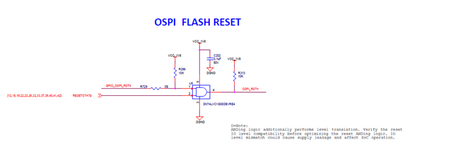
In case ANDing logic is not used and the processor Main
Domain warm reset status output (RESETSTATz) is used to
reset the attached device, ensure the IO voltage level of
the attached device matches the RESETSTATz IO voltage
level. A level translator is recommended to match the IO
voltage level. A resistor divider could be used
alternatively, provided optimum impedance value of the
resistor divider is selected. If it is too high, the
rise/fall time of the attached device reset input could be more and
introduce too much delay. If it is too low, it will cause
the processor IO to source too much steady-state current during
normal operation.
Just wanted to add some background for use flash with externa reset
4. OSPI clock loopback
Place Series resistor 0R close to the LBCLKO pin near to the processor
TRM reference
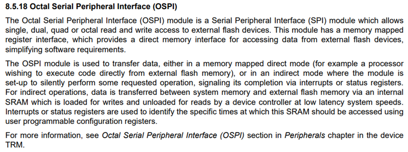
Octal Serial Peripheral Interface (OSPI)
Data Sheet reference
OSPI/QSPI/SPI Board Design and Layout Guidelines
5. DQS pulldown not provided near to Processor
Add a 1K or Similar pulldown. Refer SK schematics.
TRM Reference (AM62P)
12.4.2.4.2.1.4 External Pull Down on DQS
Per the OSPI protocol, the FLASH device drives DQS while CS is asserted. When CS is not asserted the FLASH device presents HiZ on DQS. When configured to use DQS, the controller uses the DQS as a clock, which samples the incoming data into a FIFO. Noise on the DQS when it is HiZ can cause spurious false triggering of the FIFO and filling it with invalid data. There is no way to clear this data except to reset the OSPI module.
To avoid this issue, it is recommended to add a pull down on the DQS line. During device wakeup, before the IO ring is configured properly, the CS to the FLASH device is HiZ. Depending on the actual level of the CS line the FLASH device might drive the DQS High, Low or HiZ. A pull down on DQS forces the DQS input to Low, but the DQS might still be High or in the presence of noise there might be transitions between Low and High. This again can cause the same issue of capturing garbage data in the Controller FIFO.
To avoid this issue it is recommended to release the OSPI from reset only after the IO ring is configured properly.
6. What is the default drive strength and can the drive strength be controlled?
These are typically about 60 ohms, but the customer should be using the IBIS model to determine the drive strength of the pins.
The drive strength must remain in the default state since this is the only condition used during timing closure of the peripherals.
Note: These recommendations are applicable for AM64x family of processors.
Additional information on board design
Reference Links
Regards,
Sreenivasa

Hi Board designers,
Follow below link.
The explanation is for AM62L that supports interfacing to x2 device.
Some of the placement guidelines can be followed for all devices.
Regards,
Sreenivasa
Hi Board designers,
Tap mode or PHY mode
OSPI0 offers two data capture modes, PHY mode and Tap mode.
PHY mode uses an internal reference clock to transmit and receive data via a DLL based PHY, where each reference clock cycle produces a single cycle of OSPI0_CLK for Single Data Rate (SDR) transfers or a half cycle of OSPI0_CLK for Double Data Rate (DDR) transfers. PHY mode supports four clocking topologies
for the receive data capture clock. Internal PHY Loopback - uses the internal reference clock as the PHY receive data capture clock. Internal Pad Loopback - uses OSPI0_LBCLKO looped back into the PHY from the OSPI0_LBCLKO pin as the PHY receive data capture clock. External Board Loopback - uses OSPI0_LBCLKO
looped back into the PHY from the OSPI0_DQS pin as the PHY receive data capture clock. DQS - uses the DQS output from the attached device as the PHY receive data capture clock. SDR transfers are not supported when using the Internal Pad Loopback and DQS clocking topologies. DDR transfers are not supported when using the Internal PHY Loopback or Internal Pad Loopback clocking topologies.
Tap mode uses an internal reference clock with selectable taps to adjusted data transmit and receive capture delays relative to OSPI0_CLK, which is a divide by 4 of the internal reference clock for SDR transfers or a divide by 8 of the internal reference clock for DDR transfers. Tap mode only supports one clocking topology for the
receive data capture clock. No Loopback - uses the internal reference clock as the Tap receive data capture clock. This clocking topology supports a maximum internal reference clock rate of 200 MHz, which produces an OSPI0_CLK rate up to 50 MHz for SDR mode or 25 MHz for DDR mode.
OSPI0 PHY Mode supports data transfer With PHY Data Training or OSPI0 Without Data Training
OSPI0 Tap Mode supports data transfer Without Data Training
Please refer to the OSPI timing section in the latest processor-specific data sheet to better understand the modes supported.
Have you read the OSPI chapter in the TRM and the "OSPI and QSPI Board Design and Layout Guidelines" section in the AM64x datasheet? The guidelines provided in the datasheet describes two connection topologies when the attached device doesn't have a DQS output. You need to understand the difference between these options and decide which is best for your attached device. I suspect the External Board Loopback connection topology would be the best option for your application. Next you need to decide if you are planning to operate the interface in data training mode or without data training. If you decide to use the interface without data training, you need to use the switching characteristics of the AM64x device and the switching characteristics of the attached device to perform a timing analysis of the interface by including actual PCB trace delays to verify none of the AM64x or attached device timing requirements are violated.
Regards,
Sreenivasa
Hi Board Designers,
AM625: Disturbance on OSPI CLK connected to SPI NOR (Connecting OSPI to more than x1 (multiple) devices)
I personally think it is a mistake providing multiple chip select pins on this peripheral. It is misleading and makes someone think they can connect multiple devices, when this implementation is very problematic.
The problem with connecting multiple devices is related to your observation on the clock. You see this distortion on the source end of the signal trace because the output buffer has about the same source impedance as the signal trace. When the signal changes from low to high or high to low, the voltage applied to the signal is divided by the ratio of output buffer source impedance and the signal trace impedance. It is basically a voltage divider that results in a mid-supply voltage being applied to the signal. This mid-supply voltage propagates down the signal trace until it encounters a high-impedance or open-circuit, where the mismatch in impedance results in an in-phase reflection that causes the voltage at the far end to make a continuous transition from VDD to VSS or VSS to VDD. This reflection returns back to the source, where the voltage at the source will not continue to VDD or VSS until this reflection has returned. The length of the mid-supply step function will be equal to two times the propagation time of the clock signal trace. The step function gets shorter as you get closer to the end of the signal trace, but not completely gone until the very end.
A device connected anywhere other than the far end of the signal trace will observe the same step function on the clock signal. Connecting a device clock input anywhere in the middle of a clock signal trace is a very bad design practice because there is a good chance the output of the clock input buffer of this device will generate internal clock glitches when this mid-supply voltage pauses near the switching threshold of the input buffer. You cannot split the signal trace into two paths without creating impedance discontinuities which also causes signal distortion. Inserting buffers will resolve the impedance mismatch issue but inserts delay in the clock path, which may cause a timing violation because the peripheral was timing closed assuming a direct connection without any buffer delays.
Connecting your NOR memory device to the middle of the clock signal was a mistake. You must resolve this issue by disconnecting any signal trace that extends beyond the attached device to prevent any internal clock glitch issues.
Most of the AM62x pins power-up turned off, so you need include external pull resistors to hold any attached device inputs in a valid logic state until the IOs and associated peripheral module has been initialized by software. You should never allow CMOS inputs to float. this is especially true for the AM62x inputs. All AM62x inputs which have been enabled must be held in a valid logic state that is above the VIHSS or VILSS as defined in the respective electrical characteristics section of the datasheet. The AM62x device could be damaged if your design allows any enabled inputs to float to mid-supply voltages for an accumulated period of time over the life of the product.
Please note that there are signal integrity issues that must be considered when attaching multiple devices. The data transfer rate can be reduced to allow time for the data signals to settle, but attaching a single clock signal to multiple devices is problematic.
It is not possible to distribute a single clock to multiple devices via fly-by topology without the risk of producing internal glitches on any device connected in the middle of the clock signal trace even if connected without creating stubs. It may be possible to minimize this concern by using a T topology, but it must be implemented properly and verified using signal integrity simulations.
The best way is to ensure there are no clocking issues is to insert a 1:n clock buffer in the clock signal path, which introduces significant delay and reduces the data transfer rates for the entire interface.
In my opinion, the only way to reliably achieve the data transfer rates wanted for this interface is to limit the connectivity options to a single external memory device with point to point connections.
Regards,
Sreenivasa
Hi Board Designers,
Useful FAQs
[FAQ] TDA4VM: Is there a guide to choosing the right OSPI Flash parts that are supported on Jacinto 7?
[FAQ] OSPI FAQ for Sitara/Jacinto devices
Jacinto7 HS Device Flashing Solution
https://www.ti.com/lit/an/spracz6/spracz6.pdf
OSPI NOR flash debug support on AM6x and TDA4VEN
https://www.ti.com/lit/an/sdaa066/sdaa066.pdf
Regards,
Sreenivasa
Hi Board designers,
Information related to clock pulldown
e2e.ti.com/.../faq-am625-what-s-the-purpose-for-the-pull-down-r-on-mmc_clk
May I know what the purpose for the pull down R on MMC_CLK signal on TI EVM? May I know what the purpose for the pull down R on MMC_CLK signal on TI EVM?
Most of the IOs associated with the AM62x device default to the off state, which means any attached device input without an internal pull resistor would be floating until software configures the pin to drive the signal. We use an external pull-down rather than an external pull-up since the clock signal is held in a low logic state when paused.
Because there are cases where the clock is stopped or paused in a low logic state and the pull-down option is consistent with this logic state.
Regards,
Sreenivasa
Hi Board designers,
Information related to clock measurement
What you observe on this signal depends on where you connected the probe, the bandwidth of your probe/scope, and quality of your scope probe ground.
You will need a very high bandwidth probe and scope to observe short over-shoot, under-shoot, and non-monotonic events on the signal. I recommend using a low capacitance FET probe with a very-very short low loop inductance ground.
You will see a mid-supply step on the signal when probing near the source. This occurs because the output impedance of the MMC0_CLK output buffer, series termination resistor, and characteristic impedance of the PCB signal trace creates a voltage divider. The voltage divider output is applied to the source end of the PCB signal trace. This voltage propagates down the trace to the far end where it encounters a high impedance load which causes a in-phase reflection that returns to the source. Therefore, the voltage transition observed on the far end will be a continuous transition between VSS and VDD. The is not the case for the source end, as it steps to a mid-supply determined by the voltage divider values and the transition only continues to VDD or VSS once the reflection returns from the far end. You need to select a series resistor value that allows the MMC0_CLK pin to step through the voltage of (VDDSHV4 / 2) without pause. I suggest the step observed on the MMC0_CLK pin should be at least 200mv above (VDDSHV4 / 2) on the rising edge and at least 200mv below (VDDSHV4 / 2) on the falling edge.
Regards,
Sreenivasa
Hi Board designers,
Information related to supported OSPI0 module CS for boot.
Regards,
Sreenivasa
Hi Board designers,
Additional information regarding the series resistors and pulls
AM62A3: Pull down on DQS pin
Does AM62A OSPI_DQS pin require a 100k pull-down when external loopback is used? Will a 100k pull-down be detrimental to the external loopback function?
TDA4 design review feedback from TI: "Recommend to have weak (10K-ohm) pull-up resistors on CSn, DQ2/W#, and weak (100k-ohm) pull-down resistor on CLK and DQS"
Any AM62Ax input buffer that gets turned on must never be allowed to float to a mid-supply potential. The DQS signal is only driven by the attached OSPI memory device when chip select is active, so an external pull-down resistor is required to hold the AM62Ax DQS input to a valid logic level when not driven by the attached OSPI device.
The 100k resistor value recommended by the automotive team may be too high to hold the signal in a valid logic state during the undriven period when the product is exposed to an environment with high electrical noise. I would prefer the see you use a 10k ohm pull-down.
The 10k ohm pull-down will not have any significant impact on timing of an actively driven signal as long as the pull-down is placed on the signal trace such that it doesn’t create a stub.
You may need to also include external pulls on the other signals since the AM62Ax IOs associated with OSPI will be turned off by default. The external pull resistors may be needed to hold the inputs of the attached OSPI memory device in a valid logic state.
How to reduce SPICLK EMI noise
I am considering suppressing EMI noise caused by SPI_CLK.
Is there any reduction method other than the following?
-Shorten the CLK line.
-Dull CLK by inserting a resistor or a capacitor on the order of pF.
-Lower the impedance of the power supply and signal ground.
All of these option potentially have an effect on interface timing. The best option of the three mentioned is reducing overall length of the clock trace. The worst option is reducing supply impedance, as this will effect all IOs sharing a common IO power rail.
Which SPI are you asking about, McSPI or OSPI?
The maximum operating frequency of McSPI is much lower than OSPI, so there is a much better change for it to have enough timing margin to support a slower clock transition. I would not recommend this for OSPI unless you reduce the operating frequency significantly lower than its maximum operating frequency.
The timing parameters provided in the datasheet are based on the conditions defined at the beginning of each peripheral timing section. You need to ensure your design is compliant to all of these conditions and parameters. We recommend performing a timing analysis of each peripheral using switch characteristics of each device along with actual PCB delays to confirm all timing requirements are met.
As mentioned before, increasing the inductance of the IO power supply will effect all other IOs powered from the respective IO power rail. TI does not recommend this approach and we will not be able to support any issues resulting from this approach.
Your best option would be insert a low pass filter on clock signal near the source to slow the rise/fall of the clock signal. However, you will need to make sure the delay inserted by the filter does not causing any timing violations of this peripheral.
By mounting a 100pF capacitor near the output of the microcomputer, we were able to significantly reduce noise.
Waveform timing doesn't seem to matter, but are there any other risks to this?
Timing closure of each McSPI interfaces was performed with maximum load capacitance of 12pF. So there is a good chance the 100pF load will delay the clock and cause the timing parameter values defined in the datasheet to be invalid. So you will need to characterize McSPI timing with this load and confirm there is still enough margin for the interface.
I will need to ask our IO design team if the 100pF load on SPI_CLK will cause any long-term reliability issues.
We haven’t done IO reliability assessment with loads this large. One potential problem could be degradation due to HCI/CHC when driving larger loads. Therefore, connecting a 100pf capacitor SPI_CLK is not recommended.
There is a Timing Conditions table at the beginning of each peripheral timing section in the datasheet, where the maximum capacitance is defined. Your system should be designed to be compliant to the max capacitance defined in the respective Timing Conditions table.
Output load capacitance means that it is very close to the output of AM6441, so is it no problem to put a capacitor in front of the 22Ω resistor? The timing chart meets the requirements.
Also, since the distance between TMS320 and AM6441 is about 20 cm, it is an experimental result that it is better to insert a capacitor to improve EMS and EMI performance.
How can I improve the EMS and EMI performance when the capacitor is set to 12pF or less?
The max output load capacitive defined in the datasheet is the combination of everything connected to the pin.
Connecting a 100pf capacitor directly to the output buffer causes large peak current to flow through the AM64x power rails and output buffer to the capacitor. This large capacitive load applies more stress to the output buffer than expected and introduces larger than expected ground bounce which introduces noise into the entire AM64x device.
Inserting a series resistor before any discrete capacitor load will reduce the current that flows through the AM64x power rails and output buffer. However, the RC circuit would need to be placed near the AM64x device to be effective in reducing the signal slew rate which is what you are trying to do to reduce EMI.
EMI issues is a typically a system implementation issue and has many variables which influence the profile of radiated emissions. PCB layout issues are the mostly likely contributor. For example, a common contribution to EMI has been seen when customers route signals through board to board connectors or board to cable connectors without low loop inductance return ground paths which can cause signals to radiate noise. Is the SPI_CLK signal routed such that it has a low impedance return reference along the entire path of the signal? For example, does the signal cross any split reference planes or does it transition from one reference plane to another reference plane without a nearby a stitching via or stitching capacitor?
Regards,
Sreenivasa
Hi Board designers,
Additional information
Since the flash size in bytes for the customer is 2Gb or 256 MB, so, in this case the following applies.

Does the following meet with the Flash part chosen?
Customer change to same OSPI flash as EVM board, now it can successful boot up.
Regards,
Sreenivasa
Hi Board designers,
Refer below link for memory performance:
AM62x MCU+ SDK 11.00.00
Summary:
r5f0-0:
| Data size(MiB) | Write speed(MiBps) | Read speed(MiBps) |
|---|---|---|
| 1 | 0.44 | 247.40 |
| 5 | 0.44 | 248.68 |
| 10 | 0.45 | 248.83 |
| DQS Tuning Algorithm | Tuning Time (ms) |
|---|---|
| Default Tuning Window | 3.59 ms |
| Fast Tuning Window | 1.15 ms |
a53 :
| Data size(MiB) | Write speed(MiBps) | Read speed(MiBps) |
|---|---|---|
| 1 | 0.45 | 325.77 |
| 5 | 0.45 | 326.94 |
| 10 | 0.45 | 327.08 |
| DQS Tuning Algorithm | Tuning Time (ms) |
|---|---|
| Default Tuning Window | 2.98 ms |
| Fast Tuning Window | 0.97 ms |
r5f0-0:
| Data size(MiB) | Write speed(MiBps) | Read speed(MiBps) |
|---|---|---|
| 1 | 2.06 | 46.75 |
| 5 | 2.06 | 46.76 |
| 10 | 2.06 | 46.76 |
| Non-DQS Tuning Algorithm | Tuning Time (ms) |
|---|---|
| Default Tuning Window | 1.12 ms |
| Fast Tuning Window | 0.62 ms |
a53 :
| Data size(MiB) | Write speed(MiBps) | Read speed(MiBps) |
|---|---|---|
| 1 | 2.58 | 57.02 |
| 5 | 2.58 | 57.04 |
| 10 | 2.58 | 57.04 |
| Non-DQS Tuning Algorithm | Tuning Time (ms) |
|---|---|
| Default Tuning Window | 0.96 ms |
| Fast Tuning Window | 0.53 ms |
Regards,
Sreenivasa
Hi Board designers,
Inputs related to On-board flash programming
can we use this way to program AM64x boot SPI FLASH?
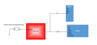
When we want to program,we short the jumper to short the MCU_PORz reset to GND,to let AM64 all pins to initial states,which can release the QSPI pins. Then we use socket connet to Programmer to download program for QSPI flash.The topology is two master with one slave.
Can this work or and any point to concern?
There will not be any issue sourcing our pins at the same IO voltage as the associated IO power rail, assuming they ensure the external programmer never applies any potential to the OSPI signals until our device is powered and held in reset. However, the connector they are planning to add for the programmer could create signal integrity problems for normal operation of the OSPI peripheral. The connector would need to placed between the processor and the memory device with the signal traces routed from the processor to the programming connector and them to the memory device such that the programming connector does not add any stubs to the OSPI signals. The signal traces from the processor to programming connector would be stubs when sourcing the OSPI signals from the programmer, but the programmer could be slowed down to provide enough time for any reflections introduced by the stubs to settle before capturing data. They may need to have a way to disconnect the clock stub during programming because reflections on the clock could create internal glitches that over-clock the state-machines in the memory device.
Thanks for the reply.I have already tested on the demo board and can work well.When I layout for the new board,I will minimize the stub for 1 and 2.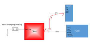
Regards,
Sreenivasa
Hi Board designers,
Inputs related to AM625: Flash compatibility
Giga devices are a fast-growing memory supplier. So can you please help compatibility for below.
NAND flash:
GD5F4GM7xExxG family (GD5F4GM7REYIG, GD5F4GM7REWIG, GD5F4GM7REBIG, GD5F4GM7UEYIG, GD5F4GM7UEWIG, GD5F4GM7UEBIG, GD5F4GM7REYJG, GD5F4GM7UEYJG)
NOR flash:
GD25LX512MEBARY
There is an FAQ we have for OSPI device selection. Dependign on how it will be used in the system there are many considerations that need to be taken.
https://e2e.ti.com/support/processors-group/processors/f/processors-forum/1181116/faq-ospi-faq-for-sitara-jacinto-devices
Please note, the flashes which have been tested on the TI EVM are:
Serial OSPI NOR Flash: S28HS512T
Serial QSPI NOR Flash: S25HL512T
Serial OSPI NAND Flash: W35N01JWTBAG
GD25LX512MEBARY
Moreover, the mentioned flash can boot in OSPI bootmode, xSPI bootmode(fastest way for ROM to boot) and SPI bootmode. To learn about these different bootmodes, the TRM section: Initialization > Boot Modes is a must read.
Regards,
Sreenivasa
Hi Board designers,
Inputs related to xSPI boot mode
I develop my custom board with AM2432.
The schematics is designed assuming that booting is performed using SPI flash (1S-1S-1S).
Therefore, I think that SPI boot mode should be used,
but xSPI boot mode has a faster startup time than SPI boot mode.
What is the difference between SPI and xSPI boot modes?
You can consider xSPI as an enhanced standard built upon traditional SPI. As you mentioned it will have a faster boot time as it can achieve higher transfer rates compared to traditional SPI. xSPI boot mode supports 1S-1S-1S mode. You can refer to chapter 4.4.1 of TRM for more details on these boot modes.
Regards,
Sreenivasa
Hi Board designers,
FYI on byte swapping.
Does AM62P Support Byte and Word Mode Write Accesses
The AM62 OSPI Controller does not support byte swapping capability.
I would like you to refer the details of this FAQ: [FAQ] PROCESSOR-SDK-AM64X: Macronix OSPI NOR Flash Integration Guide
[FAQ] AM62x, AM62Px, AM62D-Q1, AM64x, AM275x: Understanding Flash Device ID and Manufacture ID Reads
Regards,
Sreenivasa
Hi Board designers,
Input related to OSPI0_RESET_OUT0 and OSPI0_RESET_OUT1 usage

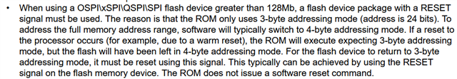
When OSPI flash memory is not used for Boot, the RESET_OUT[1:0] signals can be used to reset the OSPI flash. If OSPI flash is
used for Boot, the flash needs to be reset in tandem with SoC PORz, thus the OSPI0_RESET_OUT[0:1] signal should not be used.
Flash Reset
OSPI provides Flash reset out ports. These ports are active low and controlled thru OSPI_CONFIG_REG
register.

OSPI0_RESET_OUT0 and OSPI0_RESET_OUT1 reset output perform similar functions as a GPIO used in the SK to perform reset.
Advantage using OSPI0_RESET_OUT0 and OSPI0_RESET_OUT1 is the IOs and the control is part of the IP.
Regards,
Sreenivasa
Hi Board designers,
Input related to PYH_MASTER_PHASE_DETECT_SELECTOR_FLD in PHY_MASTER_CONTROL_REG in FSS0_OSPI_0
And could you explain more specific about PYH_MASTER_PHASE_DETECT_SELECTOR_FLD. What will be affect after change the value of this register?


The implementation is internal to the IP and we may not have any other simpler implementation to explain
this field is for synchronizing the reference and sampling clock for phy mode. It adds the necessary delay to sample the data to send to your flash.
The register is automatically configured by driver or should customer configure this register by manually or sysconfigration for custom board?
Data sheet reference:
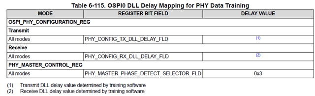
The PHY implementation has timing variability that is unique to each circuit layout. The PHY_MASTER_PHASE_DETECT_SELECTROR_FLD provides a way for the design team (internal to TI) to adjust an internal timing parameter for optimum performance. Given this is internal to the processor, customer is not expected to understand how this adjustment functions, and we have no plans to describe its function. The recommendation is for the customer to set the value defined in the datasheet to ensure the device works as expected.
Regards,
Sreenivasa
Hi Board Designers,
Input related to QSPI boot and TAP delay setting
The QSPI boot mode will boot with Tap mode, no loopback (PHY mode disabled)
Thee is Internal reference clock with Taps that the Boot ROM supports with QSPI, OSPI and XSPI(With PHY disabled) boot modes.
For QSPI and OSPI boot, OSPI0_CLK frequency is 50MHz (Where internal reference clock is 200MHz). ROM has a way of learning the optimal tap settings, which is configured during boot.
While for xSPI boot without PHY, OSPI0_CLK frequency is 25MHz.
https://e2e.ti.com/support/processors-group/processors/f/processors-forum/1548732/am625-qspi-boot-up
AM625: QSPI boot up
I understand from the e2e description of the question, that you want a customized ROM code which adapts to the flash which you are using.
Currently, the ROM code updates cannot be made. Rather any customization can be done on application/bootloader level, which is using the MCU+ SDK kit. So the current suggestion is to read TRM on how booting happens and what commands are sent, based on which the flash is decided.
Also take into account the following:
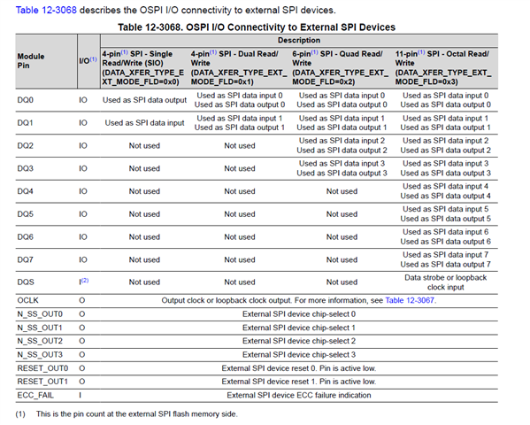
Many QSPI Flashes requires has QE bit, or the Quad Enable Bit. This is an important factor to consider as ROM does not set the QE bit.
One more thing to take care of is, in QSPI bootmode 3 byte address is required to be sent out and not 4 byte. Same follows for SPI bootmode.
So, suppose you are at application level and currently your flash is operating in 3 byte addressing mode. At a certain point if it is made to work in 4 byte addressing mode, then when you exit the application the flash might be left in 4 byte addressing mode.
And then when you try to boot from this same flash the next time, it will not boot, as 3 byte addressing is required but the flash was previously left in 4 byte addressing.
So, a good practise, is to make sure before booting, we need to make sure flash is in 3 byte addressing mode.
Since the QE = 1 is fixed, hence it would be suitable to boot in QSPI Bootmode.
Let us understand the reasoning in depth as to why the flash you are using will boot in QSPI bootmode.
The Flash datasheet/spec says the following for the 6Bh command:
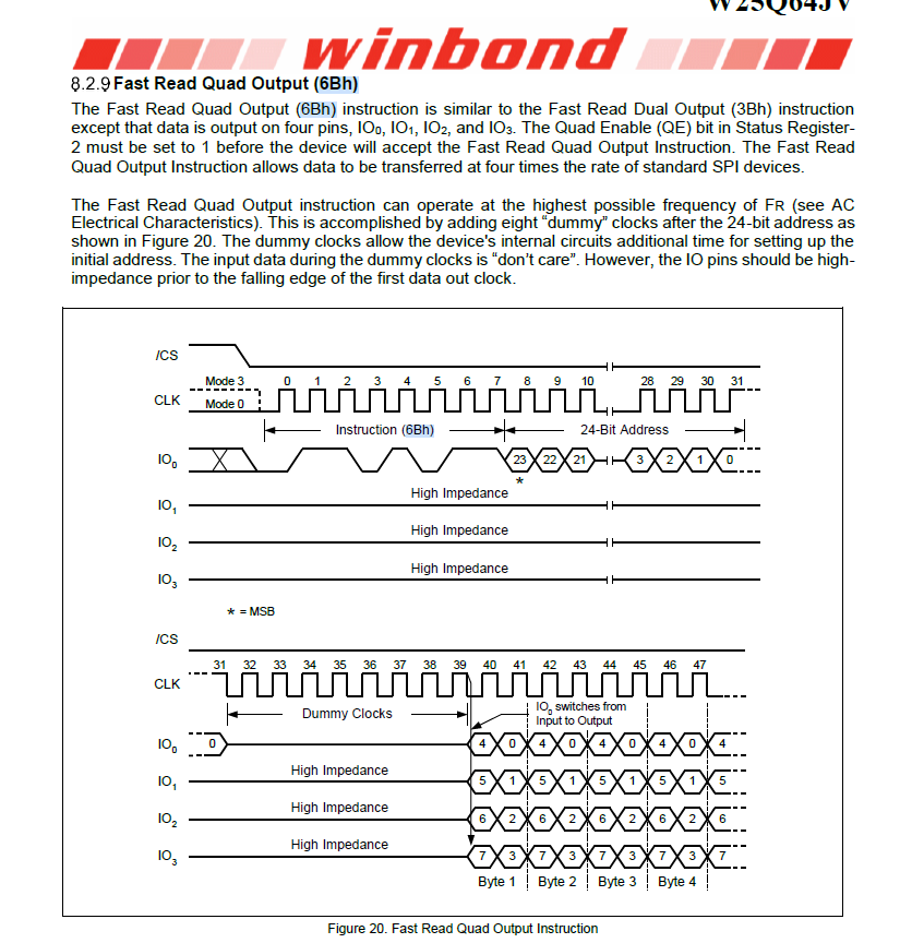
If you see above, it says the command combination will be: 6Bh + 24 bit address(3 byte address) + 8 dummy cycles
The same command is mentioned in the TRM under QSPI Boot section as well:
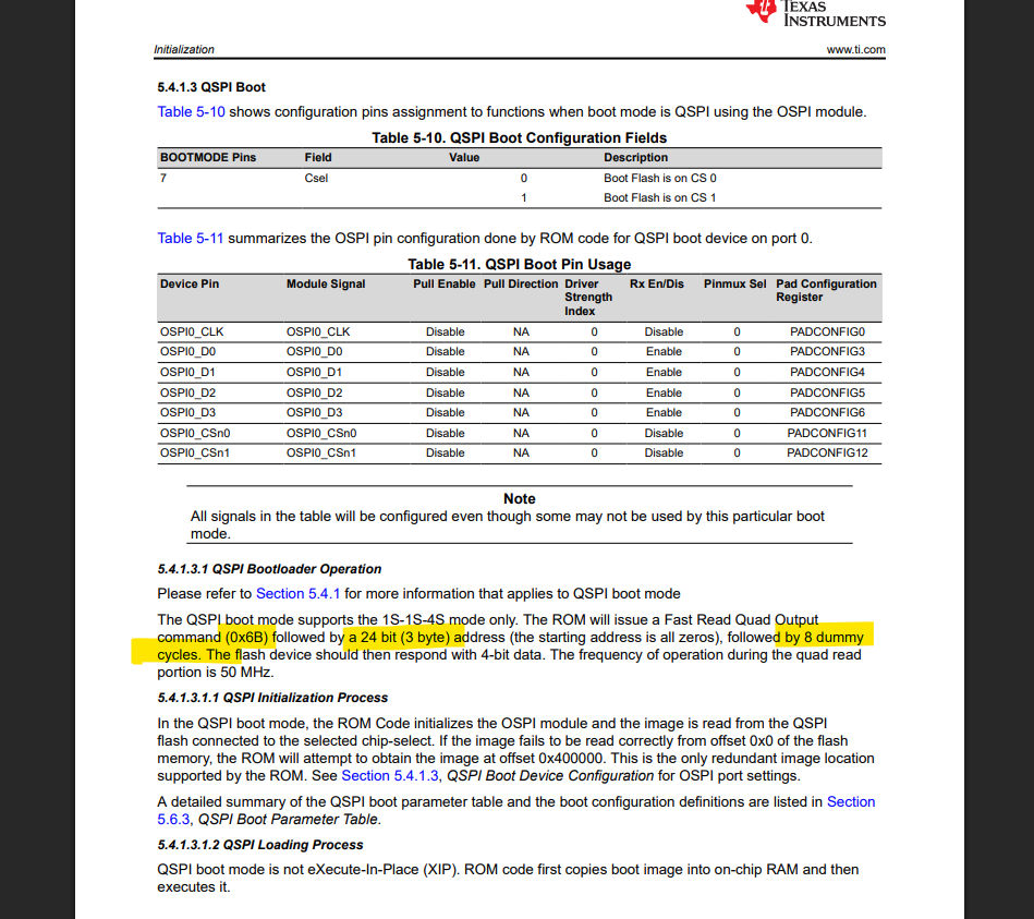
An advantage is that QE bit is already set for your flash device, hence we need not explicitly set it.
The bootcode will find valid data sampling points without the need for any data learning pattern enabled on the flash. There is no support for inserting or reading unrelated leading bytes (even any intended for data learning) to any transaction from the flash and it is not needed.
ROM does following when QSPI memory is connected.
Are you saying that the TAP Delay is optimized using the flash Manufacturer's Unique Device ID? Is that flash register first read at a slower rate with single SPI and then ROM starts iterating to find optimal TAP Delay using QSPI? It would seem that there would have to be a high level of certainty of the actual Device ID value before adjusting TAP Delay. Otherwise how would ROM know if it has achieved the optimal value?
Yes right, in order to find the appropriate Read Delay Capture value, we need to be able to read a known value back from the flash, in this case the device id value. With these flashes ROM issues a ReadID command which can only be performed in 1S mode , after finding TAP delay & programming it ..then switches to 4S.
The read Data Capture delay is adjusting to the middle value.
This middle value is not random but the middle value for the passing region.
For example, if the values 4, 3, 2, 1, 0 are being searched for and we see the green segments passing, then we pick the value 2.
ROM code uses tap mode @ 50 MHz and not PHY mode.
In ROM, the DEV_DELAY_REG is set to 0x0.
What is actually used for tap mode is the RD_DATA_CAPTURE_REG DELAY_FLD bit[4:1]. For which we (ROM) scan all possible value to find the optimum setting.
So for ROM only DEV_DELAY_REG does not matter.
After boot, in their higher level s/w, if they would need/want to enable PHY mode to increase throughput then they would need to set these
SPI Flash is initialized by ROM by reading the SFDP table only incase of xSPI Boot Mode. Refer xSPI Boot in TRM.
But ROM initializations of flash are for low frequency of <= 50MHz. SBL re-initializes the flash for highest frequency to achieve better boot performance given that the RBL is only responsible for booting the SBL but SBL will be responsible of booting Application Image with size much higher than the size of application.
Flash must support SFDP for xSPI boot mode but if it does not then they need to change the boot mode to OSPI/QSPI/SPI boot mode where the read commands of the flash must be the same as the one mentioned in the TRM.
I suggest you to go through TRM chapter for better understanding.
wrote the steps to boot full Linux from OSPI (64MiB) on AM64x GP EVM.
The procedure should apply to SPI/QSPI/OSPI MTD/UBI/UBIFS Linux booting in general.
a couple of quick general comments;
Please use this guidance for selection of the flash for your project:
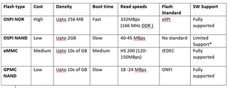
OSPI, GPMC interfaces are same across AM62, AM62A and AM62P. eMMC interface on AM62P supports upto HS400 projects and AM62/AM62A supports only HS200 speeds.
Regards,
Sreenivasa
Hi Board designers,
Inputs related to BBM
Understand how and where BBM(bad block management) is implemented in our MCU+ SDK offering: [FAQ] AM62A7: Bad Block Implementation for NAND Flash Parts
Regards,
Sreenivasa
Hi Board designers,
Inputs related to tap mode
Half level meaning, the first bit voltage rises to 1.5-1.6 V is held there for few nanoseconds and then it rises to 1.8 V
It looks like you’re using protocol 8d-8d-8d (disabled phy) but using divider 4—which means you are in tap mode. For tap mode to work in 8d-8d-8d divider has to be 8.
I set Dummy Clocks(CMD) = 3 and Dummy Clocks(READ) = 24 - the same number as for the Flash memory.
I can not find a parameter named: “Number Of Dummy Cycles In Octal Mode” or “Read id dummy cycles for octal mode” under the Sysconfig /
FLASH section. Is that the “Mode Clocks (READ)” ?

So I located & set “Number of Dummy Cycles in Octal Mode” parameter from 4 to 3. I did not change any OSPI registers content.
To summarize:


I now do not observe the OSPI half level read issue ( retaining the dq4 at around 1.3 V for 6-8 ns) upon hitting the breakpoint at line 123 in ospi_flash_dma.c.

This new result does indicate that correct divider 8 makes issue go away for tap mode.
Regards,
Sreenivasa
Hi Board designers,
Inputs related to OSPI VPP pin connection
AM2432: SBL OSPI question about ospi flash voltage characteristics and ospi clock voltage
The third image is the waveform when powering on after setting the boot mode to OSPI, showing the RBL loading SBL.

When set to 8D-8D-8D mode, the OSPI clock voltage level drops to about 2.2 to 2.4V, which raised a question whether a 1.8V device must be used.
According to the IS25LX256 chip manual,
VPP must be connected to a pull-up resistor when it's an Optional Device, and must be left floating when it's a Standard Type.
When using the Standard Type, I inserted a pull-up resistor (R105 in the schematic) to VPP, which caused the OSPI0_CLK waveform to become abnormal in OSPI mode.
I confirmed that OSPI0_CLK outputs 3.3V normally by removing the pull-up resistor (R105).
Regards,
Sreenivasa
Hi Board Designers,
Inputs related to OSPI0_INT
(+) AM625: OSPI_INTn connection and usage - Processors forum - Processors - TI E2E support forums
AM625: OSPI0_INTn OSPI_INTn connection and usage
So there are two modes to transfer data as per the Datasheet and MCU PLUS SDK drivers guide. I have attached a snapshot below, kindly check.
So the OSPI_INT pin can be used to signal completion of the transferred data.
From the above connection we can see that OSPI_CSN0 can be used as a chip select line to the OSPI flash part.
But, OSPI_CSN2 can be used to signal the completion of data transfer via Interrupt.
Regards,
Sreenivasa