This thread has been locked.
If you have a related question, please click the "Ask a related question" button in the top right corner. The newly created question will be automatically linked to this question.
Dear Sir,
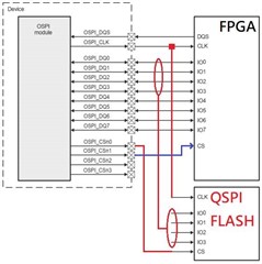
There is "only one" OSPI interface (OSPI0) on AM64x platform and two CS are supported.
Customer uses OSPI to connect FPGA with high speed high frequency communication (OSPI PHY Mode DDR) and same OSPI with different CS is connected onto QSPI flash for booting and data storage.
The concern is the traces and capacitor loading on QSPI flash could affect the high speed communication between AM64x and FPGA.
Is there any recommendation or solution to reduce the affect from additional components on the same OSPI interface?
How to avoid the impact if the additional component cannot be removed? Will adding buffer or analog switch be helpful?
BR, Rich
Hello RIch,
Thank you for the query.
Is there a block diagram that customer can share on the planned implementation.
Any thoughts on the distance expected between the devices.
Regards,
Sreenivasa
Sreenivasa,
A simple block diagram as below.
The distance of FPGA could be up to 5000 mils.
QSPI flash could be shorter, maybe around 2000~3000 mils.
BR, Rich
Hello RIch,
Thank you for the reply.
Let me review and provide my inputs.
The challenge i see is sharing the interface pins and associated signal integrity issue affecting the performance.
Regards,
Sreenivasa
Hello Rich,
Thank you for following on his.
I am reviewing the requirements and will share the recommendations at the earliet.
Regards,
Sreenivasa
Hello Rich,
Please refer below comments.
Please note that there are signal integrity issues that must be considered when attaching multiple devices. The data transfer rate can be reduced to allow time for the data signals to settle, but attaching a single clock signal to multiple devices is problematic.
It is not possible to distribute a single clock to multiple devices via fly-by topology without the risk of producing internal glitches on any device connected in the middle of the clock signal trace even if connected without creating stubs. It may be possible to minimize this concern by using a T topology, but it must be implemented properly and verified using signal integrity simulations.
The best way is to ensure there are no clocking issues is to insert a 1:n clock buffer in the clock signal path, which introduces significant delay and reduces the data transfer rates for the entire interface.
In my opinion, the only way to reliably achieve the data transfer rates wanted for this interface is to limit the connectivity options to a single external memory device with point to point connections.
Regards,
Sreenivasa
Sreenivasa,
Thanks for your comments, I will discuss this with customer.
BR, Rich
Hello Rich,
Noted and thank you. Looking forward to the customer comments.
regards,
Sreenivasa
Hello Rich,
Please refer below thread
Please let me know i can close the thread.
Regards.
Sreenivasa
Hello Rich,
I have not heard from you and closing the thread.
Regards,
Sreenivasa