This thread has been locked.
If you have a related question, please click the "Ask a related question" button in the top right corner. The newly created question will be automatically linked to this question.
In looking at the schematic for the SK-AM243 (PROC109E3_SCH.pdf), I see it's using the Infineon S25HL512TFAMHI010 QSPI flash device. If I'm looking at this correctly, it doesn't meet timing, please correct me if I'm wrong.
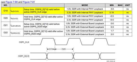
I pasted below two snippets, first one from the Infineon datasheet, the second one form the AM64 datasheet. On the AM64, when booting from QSPI flash, our ROM bootloader uses SPI mode 0, SDR, and sets the clock to 50MHz. SPI mode 0 means the AM64 latches data on the rising edge of clock. The Infineon part drives data on the falling edge of clock.
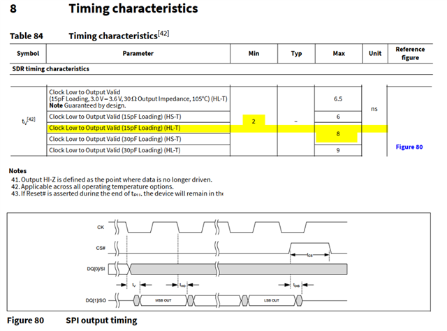
The Infineon flash device can take up to 8ns after falling edge of clock before data is valid. However, the AM64 has a 5.8ns setup time before latching data on the rising edge of clock. If you add the two together you get a total of 13.8ns. At 50MHz, we only have 10ns between falling edge and rising edge of clock. To me, this doesn't meet timing.
We're trying to find a suitable OSPI/QSPI flash that conforms to all AM64/AM24 errata's. We initially thought we could use the Infineon part but now have doubts.
I have two specific questions.
1. Can somebody confirm of show otherwise my conclusion the Infineon part on the SK-AM243 doesn't not meet timing?
2. Could somebody recommend an alternative suitable flash device?
Infineon S25HL512TFAMHI010 Datasheet
AM64 datasheet
Hi Brad,
We are looping in the right folks and should get a response up soon.
Thanks,
Mike
Hi Brad,
During boot, the device operates in TAP mode, so you are looking at the wrong table in the AM64 datasheet. the one you should be looking at is Table 7-103. OSPI0 Timing Requirements – Tap SDR Mode :
Here you will have to choose a Read Data Capture delay that helps meet the requirement. From trial and error I determined T = 3 is the smallest one to work in this case
Setting the Read Data Capture Delay to 3, and assuming your refclk is the default MAIN_PLL0_HSDIV1_CLKOUT (200MHz) then R = 5ns
Tsu = (15.4 - (0.975 * T * R)) = (15.4 - (0.975 * 3 * 5)) = 0.775ns
and hold time of
Th = = (-4.3 + (0.975 * 3 * 5)) = 10.325ns
These values meet the requirements and do not present a timing violation.
Best,
Daniel
Thank you, didn't know about TAP mode. So from the datasheet, T = OSPI_RD_DATA_CAPTURE_REG[DELAY_FLD]. I checked the TRM and this has a default reset value of 0. How do we set it to 3? Is that one of the boot parameter table values?
Is it this parameter?
Hi Brad,
That is the correct value, the Read Data Capture Delay is most of the time referred to as Tap Delay as well. I believe it should be part of the boot parameters but unfortunately I am not sure on how to modify these values. I will pull in the right expert to help you on how to do that.
Best,
Daniel
Hi Brad,
Apologies for the delayed response on this.
ROM does following when QSPI memory is connected.
Let me know if this clarifies your query.
Best Regards, Shiv
Hello Shiv,
Are you saying that the TAP Delay is optimized using the flash Manufacturer's Unique Device ID? Is that flash register first read at a slower rate with single SPI and then ROM starts iterating to find optimal TAP Delay using QSPI? It would seem that there would have to be a high level of certainty of the actual Device ID value before adjusting TAP Delay. Otherwise how would ROM know if it has achieved the optimal value?
Thank for clarifying,
Joe
Hi Joe,
Yes right, in order to find the appropriate Read Delay Capture value, we need to be able to read a known value back from the flash, in this case the device id value. With these flashes ROM issues a ReadID command which can only be performed in 1S mode , after finding TAP delay & programming it ..then switches to 4S.
Best Regards, Shiv
Thank you, Shiv. This information resolves a major timing concern! Please consider adding the details of this thread to the technical reference manual section 4.4.1. It is not documented that TAP mode is activated during boot. As a result of the errata on this family, internal pad loopback appeared to be the only configurable boot option. Based on the timing tables shown by Brad initially, not a single vendor's flash would have met timing over PVT.
Thanks again,
Joe
Hi Joe, Sure will take a note & include these details in the next TRM update. Is there anything open on this topic Or can we close this thread ?
Best Regards, Shiv