This thread has been locked.

If you have a related question, please click the "Ask a related question" button in the top right corner. The newly created question will be automatically linked to this question.

AM2432: OPEN PRU SPI example

Part Number: AM2432
Other Parts Discussed in Thread: LP-AM243, SYSCONFIG

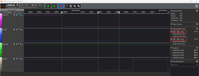
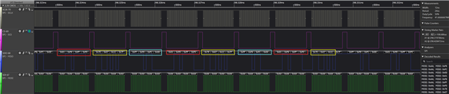
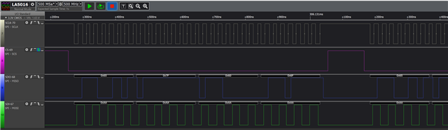
#1. The signal name is not correct in readme, from the waveform, 70 should be CS, 67 should be sclk.
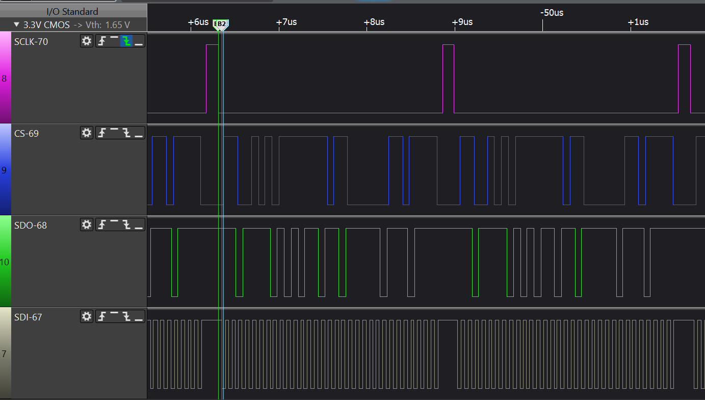
image.pngimage.png


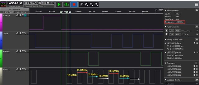
#2. The delay between SCK and DO is 20ns, it is up to 7 cycle, not 3 cycle in the readme.
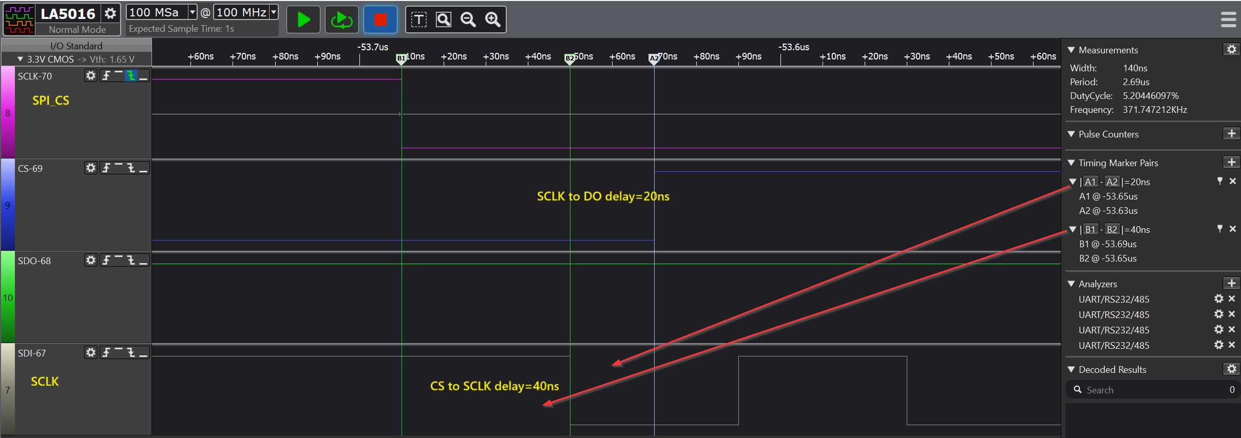
spi_delay.jpg


  • Hello Tony,

    Signal names

    I am checking with the team about the signal names, I agree that looks like it might be swapped.

    waveforms

    Let's start by making sure that this data is actually useful.

    1) Sample rate: I do not trust your logic analyzer waveforms. If the oscilloscope is only sampling at 100MHz, then you can only see in 10ns chunks minimum. I would suggest sampling at a higher rate, at least 500MHz

    2) PRU core clock rate: Can you confirm the PRU core clock frequency? If the PRU core is running slower, then the PRU clocks will also be slower. Like 200MHz (5ns/clock) or 250 MHz (4ns/clock).

    If you are using CCS, you can check the PRU clock frequency like this:
    [FAQ] PRU_ICSSG: How to check and set PRU Core Frequency in CCS?

    Regards,

    Nick

  • #1. I flashed prebuild null image into OSPI to bootup. 

    cd ${SDK_INSTALL_PATH}/tools/boot
      python uart_uniflash.py -p COM<x> --cfg=sbl_prebuilt/am243x-lp/default_sbl_null.cfg

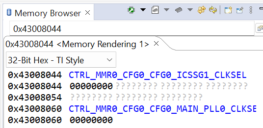
    #2. I guess it is PLL2 peripheral 1 for PRUSS from the FAQ? don't know which divider clkout for PRUSS.

    MAIN_Cortex_R5_0_0: GEL Output: Running from R5
    MAIN_Cortex_R5_0_0: GEL Output: Getting PLL Configuration...
    MAIN_Cortex_R5_0_0: GEL Output: Note: make sure the M3's RAT is programmed and the LPSC_WKUPMCU2MAIN is on
    MAIN_Cortex_R5_0_0: GEL Output: 
    Checking Main PLL
    MAIN_Cortex_R5_0_0: GEL Output: Base address: 0x00680000
    MAIN_Cortex_R5_0_0: GEL Output: PLL index: 0x00000000
    MAIN_Cortex_R5_0_0: GEL Output: PLL index register base: 0x00000000
    MAIN_Cortex_R5_0_0: GEL Output: Register: 0x00000020
    MAIN_Cortex_R5_0_0: GEL Output: Reference Divider is:     1
    MAIN_Cortex_R5_0_0: GEL Output: Feedback Divider is:      80
    MAIN_Cortex_R5_0_0: GEL Output: Fractional Multiplier is: 0
    MAIN_Cortex_R5_0_0: GEL Output: Output Divider #1 is:     2
    MAIN_Cortex_R5_0_0: GEL Output: Output Divider #2 is:     1
    MAIN_Cortex_R5_0_0: GEL Output: Number of hsdivs: 10
    MAIN_Cortex_R5_0_0: GEL Output: HSDIV #0's divider value is: 4
    MAIN_Cortex_R5_0_0: GEL Output: HSDIV #0's clkout_en: 1
    MAIN_Cortex_R5_0_0: GEL Output: HSDIV #1's divider value is: 10
    MAIN_Cortex_R5_0_0: GEL Output: HSDIV #1's clkout_en: 1
    MAIN_Cortex_R5_0_0: GEL Output: HSDIV #2's divider value is: 25
    MAIN_Cortex_R5_0_0: GEL Output: HSDIV #2's clkout_en: 1
    MAIN_Cortex_R5_0_0: GEL Output: HSDIV #3's divider value is: 15
    MAIN_Cortex_R5_0_0: GEL Output: HSDIV #3's clkout_en: 1
    MAIN_Cortex_R5_0_0: GEL Output: HSDIV #4's divider value is: 8
    MAIN_Cortex_R5_0_0: GEL Output: HSDIV #4's clkout_en: 1
    MAIN_Cortex_R5_0_0: GEL Output: HSDIV #5's divider value is: 5
    MAIN_Cortex_R5_0_0: GEL Output: HSDIV #5's clkout_en: 1
    MAIN_Cortex_R5_0_0: GEL Output: HSDIV #6's divider value is: 5
    MAIN_Cortex_R5_0_0: GEL Output: HSDIV #6's clkout_en: 1
    MAIN_Cortex_R5_0_0: GEL Output: HSDIV #7's divider value is: 5
    MAIN_Cortex_R5_0_0: GEL Output: HSDIV #7's clkout_en: 1
    MAIN_Cortex_R5_0_0: GEL Output: HSDIV #8's divider value is: 8
    MAIN_Cortex_R5_0_0: GEL Output: HSDIV #8's clkout_en: 1
    MAIN_Cortex_R5_0_0: GEL Output: HSDIV #9's divider value is: 3
    MAIN_Cortex_R5_0_0: GEL Output: HSDIV #9's clkout_en: 1
    MAIN_Cortex_R5_0_0: GEL Output: Parsed PLL configuration information.
    MAIN_Cortex_R5_0_0: GEL Output: 
    Checking Peripheral 0 PLL
    MAIN_Cortex_R5_0_0: GEL Output: Base address: 0x00680000
    MAIN_Cortex_R5_0_0: GEL Output: PLL index: 0x00000001
    MAIN_Cortex_R5_0_0: GEL Output: PLL index register base: 0x00001000
    MAIN_Cortex_R5_0_0: GEL Output: Register: 0x00000020
    MAIN_Cortex_R5_0_0: GEL Output: Reference Divider is:     1
    MAIN_Cortex_R5_0_0: GEL Output: Feedback Divider is:      76
    MAIN_Cortex_R5_0_0: GEL Output: Fractional Multiplier is: 13421773
    MAIN_Cortex_R5_0_0: GEL Output: Output Divider #1 is:     2
    MAIN_Cortex_R5_0_0: GEL Output: Output Divider #2 is:     1
    MAIN_Cortex_R5_0_0: GEL Output: Number of hsdivs: 7
    MAIN_Cortex_R5_0_0: GEL Output: HSDIV #0's divider value is: 10
    MAIN_Cortex_R5_0_0: GEL Output: HSDIV #0's clkout_en: 1
    MAIN_Cortex_R5_0_0: GEL Output: HSDIV #1's divider value is: 12
    MAIN_Cortex_R5_0_0: GEL Output: HSDIV #1's clkout_en: 1
    MAIN_Cortex_R5_0_0: GEL Output: HSDIV #2's divider value is: 5
    MAIN_Cortex_R5_0_0: GEL Output: HSDIV #2's clkout_en: 1
    MAIN_Cortex_R5_0_0: GEL Output: HSDIV #3's divider value is: 10
    MAIN_Cortex_R5_0_0: GEL Output: HSDIV #3's clkout_en: 1
    MAIN_Cortex_R5_0_0: GEL Output: HSDIV #4's divider value is: 80
    MAIN_Cortex_R5_0_0: GEL Output: HSDIV #4's clkout_en: 1
    MAIN_Cortex_R5_0_0: GEL Output: HSDIV #5's divider value is: 6
    MAIN_Cortex_R5_0_0: GEL Output: HSDIV #5's clkout_en: 1
    MAIN_Cortex_R5_0_0: GEL Output: HSDIV #6's divider value is: 16
    MAIN_Cortex_R5_0_0: GEL Output: HSDIV #6's clkout_en: 1
    MAIN_Cortex_R5_0_0: GEL Output: Parsed PLL configuration information.
    MAIN_Cortex_R5_0_0: GEL Output: 
    Checking Peripheral 1 PLL
    MAIN_Cortex_R5_0_0: GEL Output: Base address: 0x00680000
    MAIN_Cortex_R5_0_0: GEL Output: PLL index: 0x00000002
    MAIN_Cortex_R5_0_0: GEL Output: PLL index register base: 0x00002000
    MAIN_Cortex_R5_0_0: GEL Output: Register: 0x00000020
    MAIN_Cortex_R5_0_0: GEL Output: Reference Divider is:     1
    MAIN_Cortex_R5_0_0: GEL Output: Feedback Divider is:      72
    MAIN_Cortex_R5_0_0: GEL Output: Fractional Multiplier is: 0
    MAIN_Cortex_R5_0_0: GEL Output: Output Divider #1 is:     1
    MAIN_Cortex_R5_0_0: GEL Output: Output Divider #2 is:     1
    MAIN_Cortex_R5_0_0: GEL Output: Number of hsdivs: 10
    MAIN_Cortex_R5_0_0: GEL Output: HSDIV #0's divider value is: 9
    MAIN_Cortex_R5_0_0: GEL Output: HSDIV #0's clkout_en: 1
    MAIN_Cortex_R5_0_0: GEL Output: HSDIV #1's divider value is: 1
    MAIN_Cortex_R5_0_0: GEL Output: HSDIV #1's clkout_en: 0
    MAIN_Cortex_R5_0_0: GEL Output: HSDIV #2's divider value is: 9
    MAIN_Cortex_R5_0_0: GEL Output: HSDIV #2's clkout_en: 1
    MAIN_Cortex_R5_0_0: GEL Output: HSDIV #3's divider value is: 6
    MAIN_Cortex_R5_0_0: GEL Output: HSDIV #3's clkout_en: 1
    MAIN_Cortex_R5_0_0: GEL Output: HSDIV #4's divider value is: 18
    MAIN_Cortex_R5_0_0: GEL Output: HSDIV #4's clkout_en: 1
    MAIN_Cortex_R5_0_0: GEL Output: HSDIV #5's divider value is: 8
    MAIN_Cortex_R5_0_0: GEL Output: HSDIV #5's clkout_en: 1
    MAIN_Cortex_R5_0_0: GEL Output: HSDIV #6's divider value is: 8
    MAIN_Cortex_R5_0_0: GEL Output: HSDIV #6's clkout_en: 1
    MAIN_Cortex_R5_0_0: GEL Output: HSDIV #7's divider value is: 18
    MAIN_Cortex_R5_0_0: GEL Output: HSDIV #7's clkout_en: 1
    MAIN_Cortex_R5_0_0: GEL Output: HSDIV #8's divider value is: 30
    MAIN_Cortex_R5_0_0: GEL Output: HSDIV #8's clkout_en: 1
    MAIN_Cortex_R5_0_0: GEL Output: HSDIV #9's divider value is: 5
    MAIN_Cortex_R5_0_0: GEL Output: HSDIV #9's clkout_en: 1
    MAIN_Cortex_R5_0_0: GEL Output: Parsed PLL configuration information.
    MAIN_Cortex_R5_0_0: GEL Output: 
    Checking ARM 0 PLL
    MAIN_Cortex_R5_0_0: GEL Output: Base address: 0x00680000
    MAIN_Cortex_R5_0_0: GEL Output: PLL index: 0x00000008
    MAIN_Cortex_R5_0_0: GEL Output: PLL index register base: 0x00008000
    MAIN_Cortex_R5_0_0: GEL Output: Register: 0x00000020
    MAIN_Cortex_R5_0_0: GEL Output: Reference Divider is:     1
    MAIN_Cortex_R5_0_0: GEL Output: Feedback Divider is:      80
    MAIN_Cortex_R5_0_0: GEL Output: Fractional Multiplier is: 0
    MAIN_Cortex_R5_0_0: GEL Output: Output Divider #1 is:     2
    MAIN_Cortex_R5_0_0: GEL Output: Output Divider #2 is:     1
    MAIN_Cortex_R5_0_0: GEL Output: Number of hsdivs: 1
    MAIN_Cortex_R5_0_0: GEL Output: HSDIV #0's divider value is: 2
    MAIN_Cortex_R5_0_0: GEL Output: HSDIV #0's clkout_en: 1
    MAIN_Cortex_R5_0_0: GEL Output: Parsed PLL configuration information.
    MAIN_Cortex_R5_0_0: GEL Output: 
    Checking DDR PLL
    MAIN_Cortex_R5_0_0: GEL Output: Base address: 0x00680000
    MAIN_Cortex_R5_0_0: GEL Output: PLL index: 0x0000000C
    MAIN_Cortex_R5_0_0: GEL Output: PLL index register base: 0x0000C000
    MAIN_Cortex_R5_0_0: GEL Output: Register: 0x00000020
    MAIN_Cortex_R5_0_0: GEL Output: Reference Divider is:     1
    MAIN_Cortex_R5_0_0: GEL Output: Feedback Divider is:      64
    MAIN_Cortex_R5_0_0: GEL Output: Fractional Multiplier is: 0
    MAIN_Cortex_R5_0_0: GEL Output: Output Divider #1 is:     2
    MAIN_Cortex_R5_0_0: GEL Output: Output Divider #2 is:     1
    MAIN_Cortex_R5_0_0: GEL Output: Number of hsdivs: 1
    MAIN_Cortex_R5_0_0: GEL Output: HSDIV #0's divider value is: 4
    MAIN_Cortex_R5_0_0: GEL Output: HSDIV #0's clkout_en: 1
    MAIN_Cortex_R5_0_0: GEL Output: Parsed PLL configuration information.
    MAIN_Cortex_R5_0_0: GEL Output: 
    Checking Main Pulsar (R5F) PLL
    MAIN_Cortex_R5_0_0: GEL Output: Base address: 0x00680000
    MAIN_Cortex_R5_0_0: GEL Output: PLL index: 0x0000000E
    MAIN_Cortex_R5_0_0: GEL Output: PLL index register base: 0x0000E000
    MAIN_Cortex_R5_0_0: GEL Output: Register: 0x00000020
    MAIN_Cortex_R5_0_0: GEL Output: Reference Divider is:     1
    MAIN_Cortex_R5_0_0: GEL Output: Feedback Divider is:      96
    MAIN_Cortex_R5_0_0: GEL Output: Fractional Multiplier is: 0
    MAIN_Cortex_R5_0_0: GEL Output: Output Divider #1 is:     1
    MAIN_Cortex_R5_0_0: GEL Output: Output Divider #2 is:     1
    MAIN_Cortex_R5_0_0: GEL Output: Number of hsdivs: 2
    MAIN_Cortex_R5_0_0: GEL Output: HSDIV #0's divider value is: 3
    MAIN_Cortex_R5_0_0: GEL Output: HSDIV #0's clkout_en: 1
    MAIN_Cortex_R5_0_0: GEL Output: HSDIV #1's divider value is: 3
    MAIN_Cortex_R5_0_0: GEL Output: HSDIV #1's clkout_en: 1
    MAIN_Cortex_R5_0_0: GEL Output: Parsed PLL configuration information.
    MAIN_Cortex_R5_0_0: GEL Output: 
    Checking MCU 0 PLL
    MAIN_Cortex_R5_0_0: GEL Output: Base address: 0x04040000
    MAIN_Cortex_R5_0_0: GEL Output: PLL index: 0x00000000
    MAIN_Cortex_R5_0_0: GEL Output: PLL index register base: 0x00000000
    MAIN_Cortex_R5_0_0: GEL Output: Register: 0x00000020
    MAIN_Cortex_R5_0_0: GEL Output: Reference Divider is:     1
    MAIN_Cortex_R5_0_0: GEL Output: Feedback Divider is:      96
    MAIN_Cortex_R5_0_0: GEL Output: Fractional Multiplier is: 0
    MAIN_Cortex_R5_0_0: GEL Output: Output Divider #1 is:     2
    MAIN_Cortex_R5_0_0: GEL Output: Output Divider #2 is:     1
    MAIN_Cortex_R5_0_0: GEL Output: Number of hsdivs: 5
    MAIN_Cortex_R5_0_0: GEL Output: HSDIV #0's divider value is: 6
    MAIN_Cortex_R5_0_0: GEL Output: HSDIV #0's clkout_en: 1
    MAIN_Cortex_R5_0_0: GEL Output: HSDIV #1's divider value is: 25
    MAIN_Cortex_R5_0_0: GEL Output: HSDIV #1's clkout_en: 1
    MAIN_Cortex_R5_0_0: GEL Output: HSDIV #2's divider value is: 25
    MAIN_Cortex_R5_0_0: GEL Output: HSDIV #2's clkout_en: 1
    MAIN_Cortex_R5_0_0: GEL Output: HSDIV #3's divider value is: 12
    MAIN_Cortex_R5_0_0: GEL Output: HSDIV #3's clkout_en: 1
    MAIN_Cortex_R5_0_0: GEL Output: HSDIV #4's divider value is: 12
    MAIN_Cortex_R5_0_0: GEL Output: HSDIV #4's clkout_en: 1
    MAIN_Cortex_R5_0_0: GEL Output: Parsed PLL configuration information.
    MAIN_Cortex_R5_0_0: GEL Output: All PLL configurations printed.
    

    From FAQ, the ICSSG1 is currently using ICSSG1_CORE_CLK. And ICSSG1_CORE_CLK is coming from MAIN_PLL2_HSDIV0_CLKOUT, but with clock tree, there is not HSDIV0_CLKOUT, it start from HSDIV5

    Any way, I don't know how to calculate the PRU frequency.  Can you help me to confirm the PRU frequency running on my setup with upper gel output?

    #3. Regarding How do I change the PLL divider section, tells to change gel file, the gel script exist under M3, but M3 can't be connected on HS device.

    #4. With higher sample rate, the delay is a littler longer.

    The SPI_CLK frequency is not constant, it repeats in 3 closely frequency.

  • Hi Tony,

    Regarding the signal names:
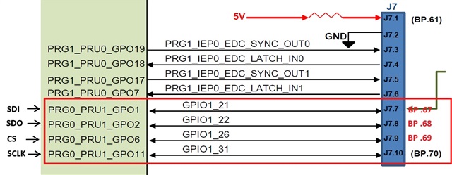
    I have verified the pin configurations and it looks correct to me. Please see the pin connections shown below based on LP-AM243 E3 schematic and the pin mapping done in the PRU code. 
      

    Please note that this pin configuration is for SPI Slave running on PRU1 of ICSSG0 of LP-AM243. If you change the PRU or the ICSSG instance, this will change the output pins for these signals.
    The same pin configuration was used while testing the SPI slave macros.

    My recommendations would be:

    1. Rechecking your connections to your scope.

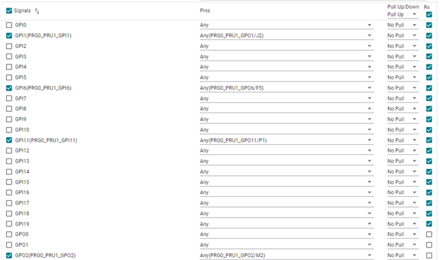
    2. Make sure your PRU1 GPIO pin muxing is done as per the sysconfig settings in the OpenPRU example. (see below)


    Regards,
    Bharath

  • Bharath,

    Thank you. I have two more questions:

    #1. How to calculate the PRU frequency? is it run at 333MHz?

    #2. I changed pru0 firmware to SPI_master_send:

    From pru1 firmware code, the SDO should be 0xCAFEC0DE, 

    SDI from PRU0 is 0xAAAAAAAA, which is correct.

    But SDO repeats in data sequence: 0xFF FB FC 00 , 0x01 FB FF F0, 0x7E 07 1C 7F.

  • Hi Tony, 

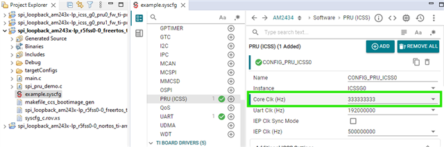
    1. An easy way to determine this would be check what's configured in the sysconfig file for the r5 core. 

      The OpenPRU example is set up in such a way that the clock, pin mux and other relevant configurations are done by the R5 core before the PRU code is loaded. By default in the example, the frequency is set to 333MHz and all timing calculations are done based on this PRU clock frequencies as already mentioned in the GitHub example documentation. 
    2. If you are changing the SPI Master side Macro to "Send" then the SPI Slave side macro should be the "Read" macro. 
      I see you have attempted to receive the packet on SPI slave side using the "transfer" macro, which has a practical limit of 12.8MHz (see SPI Slave Macros table in the github documentation). As a rule of thumb, please only use the slave side macros in combination with its corresponding master side macro and please keep an eye on the Maximum clock speeds supported. 
      For example:
      Master side macro

      Corresponding Slave side macro

      m_send_packet_spi_msb_gpo_sclk m_read_packet_spi_slave_msb_gpi_sclk
      m_send_packet_spi_lsb_gpo_sclk m_read_packet_spi_slave_lsb_gpi_sclk
      m_read_packet_spi_msb_gpo_sclk m_send_packet_spi_slave_msb_gpo_sclk
      m_read_packet_spi_lsb_gpo_sclk m_send_packet_spi_slave_lsb_gpo_sclk
      m_transfer_packet_spi_master_gpo_sclk m_transfer_packet_spi_slave_gpi_sclk

      The other combinations have not been tested. But Transfer macro along with read/send macros should theoretically work as long as the frequency is within the practical maximum frequency tested and documented. 

  • Hi Bharath,

    I change each side mode as you suggested.

    Master side: 

    PROGRAM_START:
        ; Change this label to select the type of SPI transmission.
        ; eg: SPI_master_send, SPI_master_read or SPI_master_transfer
       ; qba     SPI_master_transfer
       ; qba		SPI_master_send
    	qba		SPI_master_read

    slave side:  

    idle:
        ; update s_dataReg with test data
        mov     s_dataReg, TEMP_REG_3
        ; check if CS is pulled down. CS pin should be polled until falling edge is detected.
        m_wait_high_pulse	2, CS_PIN ; Wait for a falling edge on the CS pin
        
        ;change this label to select type of SPI transmission.
        ; eg: SPI_slave_send, SPI_slave_read or SPI_slave_transfer
        ;qba     SPI_slave_transfer
      	qba  SPI_slave_send

    The data on SDO is 0x65 7F 60 6F, which is 1bit right shifted of  0xCA FE C0 DE

    From below analyzer wave, the data should be half cycle ahead, how do you think?

  • Hi Tony, 

    As Nick had previously mentioned, I wouldn't completely trust the waveforms and decoding done on your logic analyzer at higher frequencies. 

    In the example the SPI master stores all read examples in a single 40byte buffer starting from 0x30010028 till 0x3001004C (which is overwritten once full) as defined in the following code segment:

    store_data:
        ; Write data read from SDI into R4
        sbco    &r_dataReg, c28, TEMP_REG_1, 4
        qble    reset_ptr, TEMP_REG_1, MAX_BUFFER_SIZE
        add     TEMP_REG_1, TEMP_REG_1, 4
        qba     continue

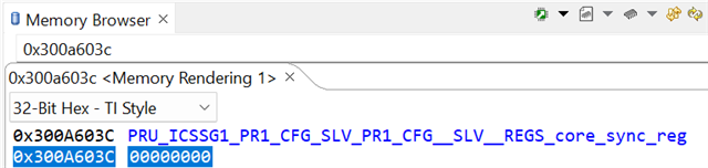
    Please check this memory buffer (you can use the ccs memory browser) to verify if the bit shift is also noticed in the PRU sampled bits.

    Regards,
    Bharath

  • Hi Bharath,

    #1. Nick doesn't trust the waveform at lower frequency, I set it back to high frequency already.

    #2. Setting:  On pru0 master side:     qba     SPI_master_transfer

                         on pru1 slave side:     qba     SPI_slave_transfer

    Got below waveform in 12.8MHz,, data are right on both SDI and SDO.

    #3. I tested different combination, if the SPI_CLK is 41.xMHz,the Slave side SDO data is 1 bit shifted.

    According to this post, under higher SPI_CLK, the delay on SDO can't meet the first SPI_CLK edge.  I think that is the root cause. 

     AM2431: Question about PRU IO Control delay 

    And can be resolved by align the first bit to CS edge other than SPI_CLK edge. How do you think?

  • Hi Tony, 

    Good to know that Transfer function is it is working at 12.8MHz. This is expected and is noted as "Practical Max. SCLK" in the Github documentation.
    For your earlier test, I see that you used Master read and Slave send macros. The Practical Max. SCLK frequencies for these macros are defined as 13.88MHz, so again it is not surprising to see issues at higher SCLK frequencies. 

    The reason for the bit shift that you have mentioned sounds correct here and might explain why the "Practical Max. SCLK" we can test the macros differ so vastly from the "Theoretical Max. SCLK" based on cycle count for when SPI Slave is sending. 

    Aligning the first bit to CS edge and subsequent bits to the SCLK should solve the bit shifting issue, but I suspect it will only work at SCLK higher than the "Practical Max. SCLK" (up to Theoretical Max) specified in the GitHub documentation. It is still not a generic solution for all possible SCLK frequencies. 

    I can file a bug report for this and based on resource availability will try to evaluate a suitable solution. 

    Regards,
    Bharath

  • Aligning the first bit to CS edge and subsequent bits to the SCLK should solve the bit shifting issue, but I suspect it will only work at SCLK higher than the "Practical Max. SCLK" (up to Theoretical Max) specified in the GitHub documentation. It is still not a generic solution for all possible SCLK frequencies. 

    I agree, I intended to let you know the possibility.