Part Number: DRA821U
Other Parts Discussed in Thread: DRA821
Follow up question to this thread:
We are using the DRA821U MCSPI interface to communicate with FPGAs on our board. Each SPI transaction is a 64-bit frame where chip select is held active across 2 32-bit bus transactions. Refer to referenced thread for detailed register settings for this interface.
In the first 32-bit cycle, we send the target Address. In the second 32-bit cycle, we either send the data to the FPGA for Write, or we receive the Read data back from the FPGA.
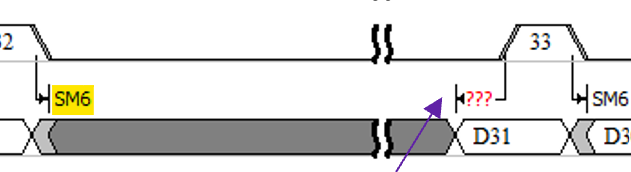
Timing diagrams for the bus in DRA821 Datasheet show processor SPI clock and data output timing relative to assertion of chip select (Figures 7-79, 7-80) - values SM8 and SM7. In our application, we are asserting/deasserting CS using CHCONF.FORCE register bit.
Question 1: Do SM8 & SM7 still apply when manually asserting chip select? If yes, does that imply that the word to transmit has to be loaded prior to asserting chipselect?
Question 2: For our application with 2 32-bit cycles with CS continuously asserted across both cycles, what's the setup and hold time of SPI_D(x)(OUT) relative to SPI_SCLK(OUT) as there is no falling edge of chip select for the 2nd 32bit bus operation?SPI Timing Question for TI.pptx Is the first bit asserted [SM8-SM7]ns before the first clock edge?