This thread has been locked.

If you have a related question, please click the "Ask a related question" button in the top right corner. The newly created question will be automatically linked to this question.

AM2434: GPMC use two CS signals

Part Number: AM2434
Other Parts Discussed in Thread: SYSCONFIG,

Hello,


We connected 2 CS signal to GPMC:

GPMC0_CSN0 and GPMC0_CSN1


In the sysconfig, i didn't find an option to configure another GPMC with GPMC0_CSN1 signal
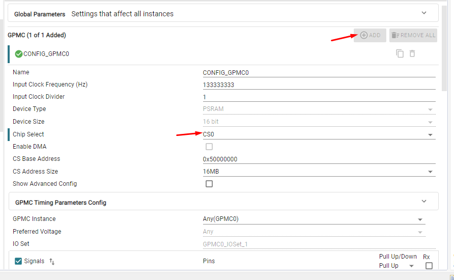
image.png

Is there any example or application note on how to configure GPMC with 2 CS signals?

thanks,

Sergei Pilipenko

  • Hello Sergei,

    Thank you for the query.

    Here is an E2E thread that warns on a possible reliability / performance impact when more than 1 CS line used ( more than one Flash memory added ) to the AM64x GPMC controller.

    Constraint on GPMC memory size and numbers of used chip selects Please consider the below excerpt of this thread:


    In the sysconfig, i didn't find an option to configure another GPMC with GPMC0_CSN1 signal

    A: Please consider that the AM2434 SoC has only one GPMC controller integrated. No other GPMC can be added in AM2434 Sysconfig flash tool.

    E2E thread on GPMC limitations in Sysconfig  - bus-width, number of chip-selects, number of instances

    Let me know if this answers your questions.

    Thanks

    Best Regards

    Anastas yordanov

  • Hello,

    According to:

    E2E thread on GPMC limitations in Sysconfig  - bus-width, number of chip-selects, number of instances

    The multiple CS should be supported in SDK 09.02.00, 

    We are using PSRAM to communicate with FPGA, SDK we are using are ind_comms_sdk_am243x_11_00_00_13 .

    Does multiple CS supported in this version?

    thanks,

    Sergei Pilipenko

  • Hi Sergei,

    Thanks for the note.

    I am looping our hardware and software GPMC experts Marc and Anil to answer.

    Please expect that a delay in the response is possible.

    Thanks

    Best Regards,

    Anastas Yordanov

  • Hello Sergei,


    MCU+ SDK supports only one GPMC chip select at a time through SysConfig.

    The SysConfig tool generates configuration for a single GPMC instance and only programs one chip select line (CS0, CS1, CS2, or CS3 — user
    selectable, but only one per project).

    Using two chip select lines simultaneously (e.g., CS0 for one memory interface and CS1 for a second memory interface) is not supported in the SDK SysConfig tool and requires manual code changes to the generated files.
    The hardware supports it — AM243X GPMC0 has four independent chip selects (CS0–CS3), each with its own independent timing, address window, and configuration registers. The driver source code also supports it through the chipSel parameter. Only the SysConfig layer and generated configuration code are limited to a single instance.


    Step-by-Step Manual Changes : 

    Prerequisites:
    - Start from a working single-CS GPMC project (e.g., gpmc_flash_io example for AM64x EVM, configured for CS0)
    - SysConfig configured for CS0 with your CS0 device settings
    - Run SysConfig once to generate base files, then apply the changes below to the generated files


    Change 1: ti_drivers_config.h

    Find:
    #define CONFIG_GPMC_NUM_INSTANCES (1U)
    Change to:
    #define CONFIG_GPMC_NUM_INSTANCES (2U)

    Change 2: ti_drivers_config.c — GPMC_HwAttrs

    The generated gGpmcAttrs[] array has one entry for CS0. Add a second entry for CS1. The two entries share the same gpmcBaseAddr (same physical controller) but differ in chipSelBaseAddr and timing.

    static GPMC_HwAttrs gGpmcAttrs[CONFIG_GPMC_NUM_INSTANCES] =
    {
    /* Instance 0 — CS0, first memory interface */
    {
    .gpmcBaseAddr = CSL_GPMC0_CFG_BASE,
    .dataBaseAddr = CSL_GPMC0_DATA_BASE,
    .elmBaseAddr = CSL_ELM0_BASE,
    .inputClkFreq = 133333333U,
    .intrNum = CSLR_R5FSS0_CORE0_INTR_GPMC0_GPMC_SINTERRUPT_0,
    .intrPriority = 4U,
    .chipSelBaseAddr = 0x50000000U, /* CS0 window: 0x50000000–0x50FFFFFF (16MB) */
    .chipSelAddrSize = GPMC_CS_MASK_ADDR_SIZE_16MB,
    .clkDivider = CSL_GPMC_CONFIG1_GPMCFCLKDIVIDER_DIVBY1,
    .waitPinNum = CSL_GPMC_CONFIG1_WAITPINSELECT_W0,
    .addrDataMux = CSL_GPMC_CONFIG1_MUXADDDATA_NONMUX,
    .timeLatency = CSL_GPMC_CONFIG1_TIMEPARAGRANULARITY_X1,
    .waitPinPol = CSL_GPMC_CONFIG_WAIT0PINPOLARITY_W0ACTIVEL,
    .timingParams = { /* CS0 device timing — from your existing generated config */ },
    .dmaRestrictedRegions = gGpmcDmaRestrictRegions,
    },
    /* Instance 1 — CS1, second memory interface */
    {
    .gpmcBaseAddr = CSL_GPMC0_CFG_BASE, /* same controller */
    .dataBaseAddr = CSL_GPMC0_DATA_BASE,
    .elmBaseAddr = CSL_ELM0_BASE,
    .inputClkFreq = 133333333U,
    .intrNum = CSLR_R5FSS0_CORE0_INTR_GPMC0_GPMC_SINTERRUPT_0,
    .intrPriority = 4U,
    .chipSelBaseAddr = 0x51000000U, /* CS1 window: 0x51000000–0x51FFFFFF (16MB) */
    .chipSelAddrSize = GPMC_CS_MASK_ADDR_SIZE_16MB,
    .clkDivider = CSL_GPMC_CONFIG1_GPMCFCLKDIVIDER_DIVBY1,
    .waitPinNum = CSL_GPMC_CONFIG1_WAITPINSELECT_W0,
    .addrDataMux = CSL_GPMC_CONFIG1_MUXADDDATA_NONMUX,
    .timeLatency = CSL_GPMC_CONFIG1_TIMEPARAGRANULARITY_X1,
    .waitPinPol = CSL_GPMC_CONFIG_WAIT0PINPOLARITY_W0ACTIVEL,
    .timingParams =
    {
    /* Set timing values to match your second device (FPGA/NOR/PSRAM) */
    .csOnTime = 0U,
    .csRdOffTime = 6U,
    .csWrOffTime = 6U,
    .advOnTime = 0U,
    .advRdOffTime = 4U,
    .advWrOffTime = 4U,
    .advAadMuxOnTime = 0U,
    .advAadMuxRdOffTime = 0U,
    .advAadMuxWrOffTime = 0U,
    .weOnTtime = 0U,
    .weOffTime = 3U,
    .oeOnTime = 1U,
    .oeOffTime = 4U,
    .oeAadMuxOnTime = 0U,
    .oeAadMuxOffTime = 0U,
    .pageBurstAccess = 0U,
    .rdAccessTime = 4U,
    .wrAcessTime = 6U,
    .rdCycleTime = 6U,
    .wrCycleTime = 6U,
    .wrDataOnMuxBusTime = 0U,
    .cycle2CycleDelay = 0U,
    .busTurnAroundTime = 0U,
    .cycleDelaySameChipSel = CSL_GPMC_CONFIG6_CYCLE2CYCLESAMECSEN_NOC2CDELAY,
    .cycleDelayDiffChipSel = CSL_GPMC_CONFIG6_CYCLE2CYCLEDIFFCSEN_NOC2CDELAY,
    },
    .dmaRestrictedRegions = gGpmcDmaRestrictRegions,
    },
    };

    Note: CS0 and CS1 chipSelBaseAddr must not overlap. With GPMC_CS_MASK_ADDR_SIZE_16MB, CS0 occupies 0x50000000–0x50FFFFFF and CS1 occupies 0x51000000–0x51FFFFFF. Both fall inside the existing GPMC MPU region — no additional MPU region is needed (see Change 4 below).


    Change 3: ti_drivers_config.c — GPMC_Params

    Add the second entry to gGpmcParams[]:

    GPMC_Params gGpmcParams[CONFIG_GPMC_NUM_INSTANCES] =
    {
    /* Instance 0 — CS0 */
    {
    .gpmcDmaChIndex = 0, /* DMA channel index for CS0 */
    .devType = CSL_GPMC_CONFIG1_DEVICETYPE_NANDLIKE, /* or NORLIKE — match CS0 device */
    .devSize = CSL_GPMC_CONFIG1_DEVICESIZE_EIGHTBITS,
    .chipSel = GPMC_CHIP_SELECT_CS0,
    .intrEnable = FALSE,
    .dmaEnable = TRUE,
    .transferMode = GPMC_TRANSFER_MODE_BLOCKING,
    .memDevice = GPMC_MEM_TYPE_NAND,
    },
    /* Instance 1 — CS1 */
    {
    .gpmcDmaChIndex = -1, /* -1 = no DMA; set to 1 if CS1 also needs DMA */
    .devType = CSL_GPMC_CONFIG1_DEVICETYPE_NORLIKE, /* match your CS1 device type */
    .devSize = CSL_GPMC_CONFIG1_DEVICESIZE_SIXTEENBITS,
    .chipSel = GPMC_CHIP_SELECT_CS1, /* ← this is the key field */
    .intrEnable = FALSE,
    .dmaEnable = FALSE,
    .transferMode = GPMC_TRANSFER_MODE_BLOCKING,
    .memDevice = GPMC_MEM_TYPE_NORLIKE,
    },
    };

    ---
    Change 4: ti_pinmux_config.c — Add GPMC0_CSN1 pin

    SysConfig only generates the GPMC0_CSn0 pinmux entry. You must manually add GPMC0_CSn1.

    In the gPinMuxMainDomainCfg[] array, add after the existing GPMC entries:

    /* GPMC0_CSn1 — manually added for CS1 support */
    {
    PIN_GPMC0_CSN1,
    ( PIN_MODE(0) | PIN_PULL_DISABLE | PIN_SLEW_RATE_LOW )
    },


    Change 5: MPU region — no change required

    The existing GPMC MPU region configured by SysConfig is:


    Change 6: Application code

    After Drivers_open(), the two GPMC handles are available as:

    /* In ti_drivers_open_close.c, Drivers_open() opens all CONFIG_GPMC_NUM_INSTANCES instances */

    extern GPMC_Handle gGpmcHandle[CONFIG_GPMC_NUM_INSTANCES];

    GPMC_Handle hCS0 = gGpmcHandle[0]; /* CS0 — first memory interface */
    GPMC_Handle hCS1 = gGpmcHandle[1]; /* CS1 — second memory interface */

    For direct memory-mapped access (NOR-like / FPGA):
    /* CS0 device at 0x50000000 */
    volatile uint16_t *cs0Mem = (volatile uint16_t *)0x50000000U;

    /* CS1 device at 0x51000000 */
    volatile uint16_t *cs1Mem = (volatile uint16_t *)0x51000000U;

    The driver programs GPMC_CONFIG7(0) for CS0 and GPMC_CONFIG7(1) for CS1 independently during GPMC_open() for each instance. Both CS windows are active simultaneously after both instances are opened.


    Important Cautions : 

    1. SysConfig regeneration overwrites manual changes
    Every time you click "Generate" in SysConfig or rebuild with the SysConfig CLI, ti_drivers_config.h, ti_drivers_config.c, and ti_pinmux_config.c are overwritten. Your manual changes to these files will be lost. Options to handle this:
    - Copy the generated files to a separate custom/ directory, rename them, and include the custom copies in your build instead of the generated ones
    - Stop using SysConfig for these files entirely after the initial generation

    2. Timing parameters per device
    CS0 and CS1 can have completely independent timing registers. Set timingParams in gGpmcAttrs[1] to values appropriate for your CS1 device. Do not copy CS0 timing blindly — the second device may have different setup/hold and access time requirements.

    3. Interrupt sharing
    Both CS instances share the same GPMC interrupt line (CSLR_R5FSS0_CORE0_INTR_GPMC0_GPMC_SINTERRUPT_0). The SDK registers only one interrupt handler per GPMC_open() call. If both instances use interrupt mode, the second GPMC_open() will attempt to re-register the same interrupt and will fail. Keep intrEnable = FALSE for at least one of the two instances, or both. Use polling or DMA transfer mode instead.

    4. WAIT pin sharing
    The GPMC WAIT0 and WAIT1 signals are shared across all chip selects. If your CS1 device uses a different WAIT pin behavior from CS0, configure waitPinNum and waitPinPol in the CS1 GPMC_HwAttrs accordingly. If both devices use the same WAIT pin with conflicting polarities, they cannot be used simultaneously.

    5. Cycle-to-cycle delay between CS switches
    When the GPMC switches from one active CS to another, the cycle2CycleDelay and cycleDelayDiffChipSel fields in timingParams control the inter-CS bus turnaround time. Set cycleDelayDiffChipSel to a non-zero value if your devices require dead time between CS transitions on the shared bus.

    Regards,

    Anil.

