This thread has been locked.

If you have a related question, please click the "Ask a related question" button in the top right corner. The newly created question will be automatically linked to this question.

AM3352: AM3352 GPMC, Async, Read timing, Setup/hold for data latch

Part Number: AM3352

Hello,


I have some questions for AM3352 GPMC timing.

1)
The below is from the datasheet, I think the start point of FA5 is strange.
I believe that the start point of FA5 should be the same as the start point of FA9 and FA10 like the red line in the below figure. Is this understanding correct? (TRM looks like having correct timing)
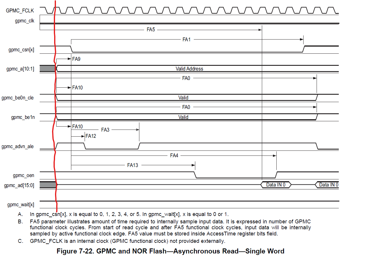

image.png


2. 
I believe that FA5 means the latching point of the read data.
But I couldn't find setup/hold timing for it on the datasheet. Do these values available on the datasheet?

Regards,
Oba

  • Hi Oba, 

    (TRM looks like having correct timing)

    Can you please tell the figure caption you are referring to? Thanks!

    Regards,

    Stan

  • Hello

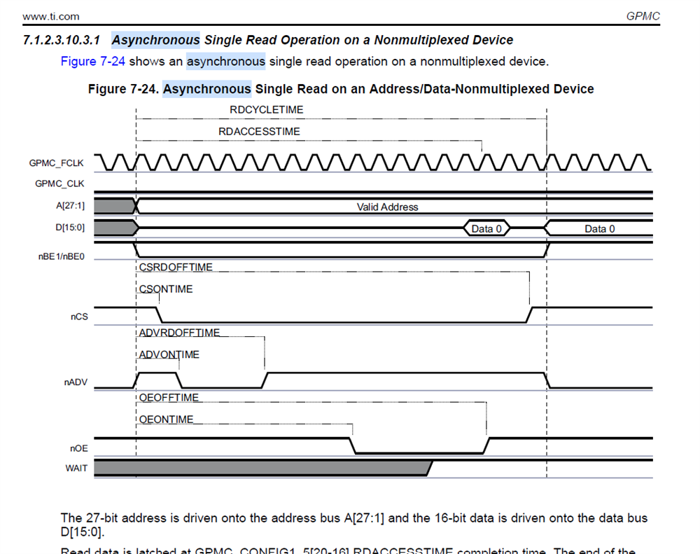
    The below comes from P643

    Today, I received an email from the customer and they are going to use multiplexed mode instead of non-multiplexed mode.
    So we should refer to the below timing charts.

    <TRM:P627>

    <Datasheet, P138>

    Regards,

    Oba

  • Hello Oba-san,

    Thank you for detailed elaboration.

    The below is from the datasheet, I think the start point of FA5 is strange.
    I believe that the start point of FA5 should be the same as the start point of FA9 and FA10 like the red line in the below figure. Is this understanding correct?

    Yes, you are right, it is a bit confusing about the starting point. The good thing FA5 is described with footnote B and on several more locations.

    The main difference between TRM and DS diagrams is that TRM shows the internal function of the controller while DS shows characterized values measured on SoC pins. TRM diagrams allows to understand better how the GPMC works and how to set registers. DS also mentions registers but also the exact timing values for the particular SoC.

    I believe that FA5 means the latching point of the read data.
    But I couldn't find setup/hold timing for it on the datasheet. Do these values available on the datasheet?

    GPMC starts reading data pins at FA5 time and continues until FA4 time. Both parameters are adjustable as shown on TRM figures.

    Best Regards,

    Stan

  • Hello Stan,

    The start point of FA5 is not still clear.
    The footnote just says "From start of read cycles", but it doesn't mention where is the start of read cycles.
    Where is it?

    Regards,
    Oba

  • Hello Oba,

    Thank you.

    The expert is on vacation this Monday.

    Please expert delay in response.

    Regards,

    Sreenivasa

  • Hi Oba,

    You are right, TRM diagrams are more accurate. FA5 starts from the start of read cycle. Read cycle starts from rising edge of FCLK (internal) after a read was issued from software.

    FA5 is RDACCESSTIME (a register setting) on TRM figures.

    Best Regards,

    Stan

  • Hello Stan,

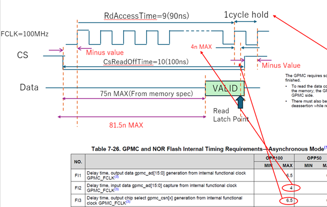
    I read the TRM and datasheet again and again. The below ppt file is my understanding for setup/hold time of read access.

    CS falling to DATA valid max time of the connected memory is 75ns.
    Then I think RdAccessTime = 9 and CsReadOffTime=1 are good configuration.
    Is this understanding correct? Could you check the timing chart?

    GPMC.pptx

    Regards,
    Oba

  • Hello Oba,

    RdAccessTime = 9 looks good. 

    1 clock hold time is related to OEOFFTIME. Usually CS is better to be released 1 clock after nOE release, however this depends mainly on memory requirements.

    Thanks,

    Stan

  • Hello Stan,

    Regarding OE and CE relation, I will check the memory spec.

    And I think we still need MIN value of FI2 and FI3, what is MIN value for them? 0ns?

    Regards,
    Oba

  • Hello Oba,

    Unfortunately if a value is missing then this parameter has not been characterized. The worst case (MAX) delay has been characterized and this value should be used in calculations as this is the guaranteed value.

    Regards,

    Stan

  • Hello Stan,

    But if FI2 has a large minus value, the setup time may not be enough 

    If  FI3 has a large minus value, the hold time may not be enough.

    I think there is no way to know if the configured timing is enough or not without the min values.

    How to think about it?

    Regards,
    Satoshi Obata


  • Hello Obata-san,

    I don't think this can have a negative value. All IO signals a synchronous to FCLK. Delays can be induced due propagation delays in the chip.

    Note that CS can be delayed, if needed, via CSONTIME and CSRDOFFTIME register bits for e.g. 1 FCLK as shown on TRM diagrams. 

    Regards,

    Stan