Hi,
I have a TMS320C6748 and I need to set the GPIO pins as outputs through the Code Composer Studio. Could anybody give me an example of a program using the GPIO as output pins. It would help me a lot...
Thanks,
Miguel.
This thread has been locked.
If you have a related question, please click the "Ask a related question" button in the top right corner. The newly created question will be automatically linked to this question.
Hi,
I have a TMS320C6748 and I need to set the GPIO pins as outputs through the Code Composer Studio. Could anybody give me an example of a program using the GPIO as output pins. It would help me a lot...
Thanks,
Miguel.
Hi Miguel,
yes, the GPIO driver code is available as a part of "C6748_StarterWare_1_20_03_03" software package. Once you install this package, under the path, C:\Program Files\Texas Instruments\pdk_C6748_2_0_0_0\C6748_StarterWare_1_20_03_03\drivers, in gpio.c, the function, GPIODirModeSet() sets the direction of gpio as input or output. Please refer to it.
If you are looking exactly the gpio example with pins configured as output, please refer to the software package "mcsdk_1_01_00_01"
path after installation
..\pdk_OMAPL138_1_01_00_01\packages\ti\csl\omapl138-lcdk\examples\gpio\src\gpio_example.c
In that example, the 7th pin of GPIO Bank[0] is configured as output pin to generate interrupts.
This code runs successfully on TMS320C6748 LCDK board.
Regards,
Shankari
-------------------------------------------------------------------------------------------------------
Please click the Verify Answer button on this post if it answers your question.
--------------------------------------------------------------------------------------------------------
Can I set the values of the High and Low logic voltages? I'm asking this, because I want to use a few GPIO pins as outputs to generate the control signals for a external multiplexer.
BTW, where are exactly the GPIO pins in the development kit? Are they in the expansion pins? Is there any picture or diagram where I could see this?
Regards,
Miguel.
Hi Miguel,
Miguel says said:Can I set the values of the High and Low logic voltages? I'm asking this, because I want to use a few GPIO pins as outputs to generate the control signals for a external multiplexer.
Yes.
Miguel says said:BTW, where are exactly the GPIO pins in the development kit? Are they in the expansion pins? Is there any picture or diagram where I could see this?
Please refer the Data sheet of the processor and the schematics of the Development Kit.
Regards,
Shankari
-------------------------------------------------------------------------------------------------------
Please click the Verify Answer button on this post if it answers your question.
--------------------------------------------------------------------------------------------------------
Could you please tell me how can I do it? Where can I find an example like that? Do I have to change anything on the registers of these GPIO pins?
Thanks a lot,
Miguel.
Hi Miguel,
In my first post, I have already answered this question like which example you can refer to as well as the name of the package.
By any chance you looked into the following which I referred to you previously?
If you are looking exactly the gpio example with pins configured as output, please refer to the software package "mcsdk_1_01_00_01"path after installation
..\pdk_OMAPL138_1_01_00_01\packages\ti\csl\omapl138-lcdk\examples\gpio\src\gpio_example.c
Download link for mcsdk_1_01_00_01 : http://processors.wiki.ti.com/index.php/L138/C6748_Development_Kit_(LCDK)#Software
Regards,
Shankari
-------------------------------------------------------------------------------------------------------
Please click the Verify Answer button on this post if it answers your question.
--------------------------------------------------------------------------------------------------------
Hi,
As Shankari mentioned, The below codes used to access the GP0[7] { bank 0 and gpio 7} in "gpio_example.c" file
/* Configure GPIO0_7 (GPIO0_7_PIN) as an output */
CSL_FINS(gpioRegs->BANK[0].DIR,GPIO_DIR_DIR7,0);
/* set the GIPO0_7 value to 0 */
CSL_FINS(gpioRegs->BANK[0].OUT_DATA,GPIO_OUT_DATA_OUT7,0);
If you wish to access the GPIO bank 4 and GPIO is 5 then
/* Configure GPIO4_5 (GPIO4_5_PIN) as an output */
CSL_FINS(gpioRegs->BANK[4].DIR,GPIO_DIR_DIR5,0);
/* Configure GPIO4_5 (GPIO4_6_PIN) as an input */
CSL_FINS(gpioRegs->BANK[4].DIR,GPIO_DIR_DIR6,1);
/* set the GIPO4_5 value to 0 */
CSL_FINS(gpioRegs->BANK[4].OUT_DATA,GPIO_OUT_DATA_OUT5,0);
/* set the GIPO4_5 value to 1 */
CSL_FINS(gpioRegs->BANK[4].OUT_DATA,GPIO_OUT_DATA_OUT5,1);
Which GPIO pins do you recommend me to use for my purpose? I need 5 GPIO pins working together to control my multiplexers, so by now I'm using GP3[2], GP3[3], GP3[4] and GP2[4], GP2[5]. Is it correct?
Also, I could not find any schematic that shows where these GPIO are. Do you have any?
Hi Shankari,
I've checked the example you told me, but I don't understand it. I didn't know that I have to use any interruption function.
In my program I made this in my main function:
GPIO_setDir(GPIO_BANK3, GPIO_PIN4, GPIO_OUTPUT); //A
GPIO_setDir(GPIO_BANK3, GPIO_PIN3, GPIO_OUTPUT); //B
GPIO_setDir(GPIO_BANK3, GPIO_PIN2, GPIO_OUTPUT); //C
GPIO_setDir(GPIO_BANK2, GPIO_PIN5, GPIO_OUTPUT); //A0
GPIO_setDir(GPIO_BANK2, GPIO_PIN4, GPIO_OUTPUT); //A1
while (1) {
GPIO_setOutput(GPIO_BANK3, GPIO_PIN4, OUTPUT_HIGH); //001
GPIO_setOutput(GPIO_BANK3, GPIO_PIN2, OUTPUT_HIGH); //101
for(inbuf_ptr=0; inbuf_ptr<BUFLENGTH; inbuf_ptr++)
{
//program
}
USTIMER_delay(ts);
//mic A
GPIO_setOutput(GPIO_BANK3, GPIO_PIN3, OUTPUT_HIGH); //111
//speaker 2-R
GPIO_setOutput(GPIO_BANK2, GPIO_PIN5, OUTPUT_HIGH); //01
GPIO_setOutput(GPIO_BANK2, GPIO_PIN4, OUTPUT_HIGH); //11
transfer(inbuffer, cancel);
USTIMER_delay(ts);
Could you please tell me if this is correct?
Thanks in advance.
Hi,
Which GPIO pins do you recommend me to use for my purpose? I need 5 GPIO pins working together to control my multiplexers, so by now I'm using GP3[2], GP3[3], GP3[4] and GP2[4], GP2[5]. Is it correct?
Is the board that you are using is TI EVM or custom board?
If custom board, Refer your schematics.
Also, I could not find any schematic that shows where these GPIO are. Do you have any?
It depends on what type of board are your referring/using it?
For e.g.,
In TI's OMAPL138 LCDK board,
GP2[4] & GP2[5] are mapped to switches (S2 and S3)
GP3[2], GP3[3] & GP3[4] are muxed with EMIFA , So those pins are used for on board NAND flash.
How about your board ?
If it is custom, then NAND flash should be in 8 bit mode for accessing the GP3[3] ...
What do you say?
..\pdk_OMAPL138_1_01_00_01\packages\ti\csl\omapl138-lcdk\examples\gpio\src\gpio_example.c
Actually, This example is used for how to access the GPIOs in input mode(interrupt based) as well output.
I'm using the OMAPL138 LCDK board, not a custom board.
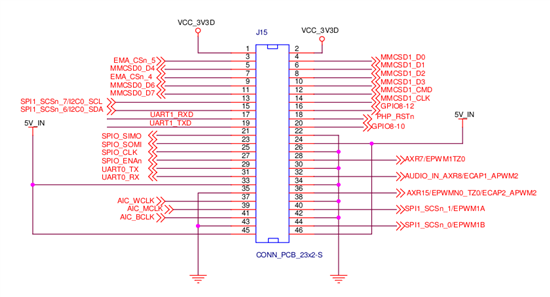
Which are the GPIO related to the J13 and J14 pins? I need 5 physical connections to plug my multiplexers. Which connectors could I use?
Also, which libraries and files on the linker I need for using the GPIO?
Regards,
Miguel.
Hi,
I'm using the OMAPL138 LCDK board, not a custom board.
Have you referred the OMAPL138 LCDK schematics any time?
Use GPIOs from J15 and ensure that will not affect any peripherals.
PFA of OMAPL138/C6748 LCDK schematics.
Hi,
The problem of J15 is that there are only two GPIO pins; GPIO8[10] and GPIO8[12] and I need three more. Where can I get them? Because there aren't any GPIO pins on J14...
Which libraries and files on the linker I need for using the GPIO?
Thanks!
Hi again,
I've seen that on J14 there are all EMA pins. Could I set a few of them as GPIO-outputs bit by bit? How can I do it? Which are the sentences on C languge for that? Which registers do I have to associate them for this purpose?
Thanks a lot,
Miguel.
Also, I have a few errors when I build the Gpio_example. I get this errors:
Description Resource Path Location Type
#20 identifier "gpioRegs" is undefined main.c /ANC line 114 C/C++ Problem
Description Resource Path Location Type
#20 identifier "psc1Regs" is undefined main.c /ANC line 198 C/C++ Problem
Description Resource Path Location Type
#20 identifier "sysRegs" is undefined main.c /ANC line 99 C/C++ Problem
How can I solve this errors?
Miguel Gaitero said:Also, I have a few errors when I build the Gpio_example. I get this errors:
Description Resource Path Location Type
#20 identifier "gpioRegs" is undefined main.c /ANC line 114 C/C++ ProblemDescription Resource Path Location Type
#20 identifier "psc1Regs" is undefined main.c /ANC line 198 C/C++ ProblemDescription Resource Path Location Type
#20 identifier "sysRegs" is undefined main.c /ANC line 99 C/C++ ProblemHow can I solve this errors?
I made this for initialize a GPIO as an output.
#include <stdio.h>
#include <c6x.h>
#include <ti/csl/cslr_dspintc.h>
#include <ti/csl/soc_C6748.h>
#include <ti/csl/cslr_gpio.h>
#include <ti/csl/cslr_syscfg0_C6748.h>
#include <ti/csl/cslr_psc_C6748.h>
int main (void){
/* Key to be written to enable the pin mux registers for write */
sysRegs->KICK0R = 0x83e70b13;
sysRegs->KICK1R = 0x95A4F1E0;
/* enable the pinmux for the GPIO bank 0 pin 7 */
sysRegs->PINMUX1 = ((CSL_SYSCFG_PINMUX1_PINMUX1_3_0_GPIO0_7)
<< (CSL_SYSCFG_PINMUX1_PINMUX1_3_0_SHIFT));
/* lock the pinmux registers */
sysRegs->KICK0R = 0x00000000;
sysRegs->KICK1R = 0x00000000;
/* first enable the GPIO in the PSC */
gpioPowerOn();
/* Configure GPIO0_7 (GPIO0_7_PIN) as an output */
CSL_FINS(gpioRegs->BANK[0].DIR,GPIO_DIR_DIR7,0);
/* set the GIPO0_7 value to 0 */
CSL_FINS(gpioRegs->BANK[0].OUT_DATA,GPIO_OUT_DATA_OUT7,0);
}
Is it correct? Do I have to do the sysRegs?
Which is the purpose of the sentence:
sysRegs->PINMUX1 = ((CSL_SYSCFG_PINMUX1_PINMUX1_3_0_GPIO0_7)
<< (CSL_SYSCFG_PINMUX1_PINMUX1_3_0_SHIFT));
I don't understand why do I have to declare this sentence if I just want to declare the pin as an output, not as a pinmux.
Thank you very much,
Miguel
Hi,
Which is the purpose of the sentence:
/* enable the pinmux for the GPIO bank 0 pin 7 */
sysRegs->PINMUX1 = ((CSL_SYSCFG_PINMUX1_PINMUX1_3_0_GPIO0_7)
<< (CSL_SYSCFG_PINMUX1_PINMUX1_3_0_SHIFT));I don't understand why do I have to declare this sentence if I just want to declare the pin as an output, not as a pinmux.
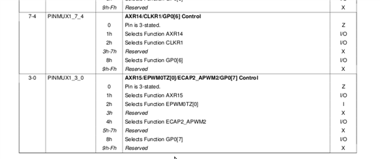
As mentioned in code comment, It is used to do pinmux (selecting GPIO peripheral) for GPIO peripheral.
From code,
CSL_SYSCFG_PINMUX1_PINMUX1_3_0_SHIFT ---> 0x0 (offset)
CSL_SYSCFG_PINMUX1_PINMUX1_3_0_GPIO0_7 ----> 0x8 (value for selecting as GPIO)
You can also write like below
sysRegs->PINMUX1 = (8 << 0) == sysRegs->PINMUX1 = ((CSL_SYSCFG_PINMUX1_PINMUX1_3_0_GPIO0_7)
<< (CSL_SYSCFG_PINMUX1_PINMUX1_3_0_SHIFT));
If you wish to access the GPIO0[6]
sysRegs->PINMUX1 = (8 << 4)
OR
sysRegs->PINMUX1 = ((CSL_SYSCFG_PINMUX1_PINMUX1_7_4_GPIO0_6)
<< (CSL_SYSCFG_PINMUX1_PINMUX1_7_4_SHIFT));
Here '0x4' is the offset of PINMUX1_7_4 and 0x8 is the value for selecting as GPIO
Please refer "pdk_OMAPL138_1_01_00_01/packages/ti/csl/cslr_syscfg0_OMAPL138.h"
Hi again,
I've seen on the schematic that there are a lot of EMA pins on J14. Could I set the EMA-D pins as GPIO-outputs? How can I do it? Which are the sentences on C language for that? Which registers do I have to associate them?
Another question: How can I set on the GPIO the High Logic voltage to 3V? And the Low Logic Voltage to 0.5V?
Regards,
Miguel.
Hi,
I've seen on the schematic that there are a lot of EMA pins on J14. Could I set the EMA-D pins as GPIO-outputs? How can I do it? Which are the sentences on C language for that? Which registers do I have to associate them?
As I told you that It is purely depends on your requirement.
If you don't want NAND flash access then you would access the EMA pins, Else try to choose some other peripheral which you are not using in your project such as SD/MMMC, EMAC(ethernet) etc.,
Another question: How can I set on the GPIO the High Logic voltage to 3V? And the Low Logic Voltage to 0.5V?
Do you have intend reason to ask this question?
I don't much expert on hw level,
Typically, It is depends IO voltage level on the processor.
Our GPIO IO level supports 3V.
In our processor, If you write logic '1' or HIGH on the GPIO, you would get 3V and If you write logic '0' or LOW on the GPIO, you would get ~0V
Hi,
The GPIO voltage levels are fine to me, thanks.
I don't need the NAND flash acces, I just any physical pin to use as GPIO and it seems I can use the EMA pins. Could you help me a bit with this? Do I just have to set the number of the GPIO pin? Or do I have to change anything to use the EMA as GPIO.
One more thing, I don't understand the memory address that has to be assigned to the GPIO. If I have 5 GPIO pins configured as outputs, do they have to be assigned to the same memory address? Is there any table where I can find the memory address for each GPIO pin?
Thanks a lot!
Miguel.
Hi Miguel,
Please refer the below ti e2e post regarding the GPIO code.
http://e2e.ti.com/support/dsp/tms320c6000_high_performance_dsps/f/115/t/341382.aspx
I wrote a GPIO code for controlling the Switch S2 from OMAPL138 LCDK.
You can create new thread for your problem and I hope it make sense that other members also get benefited,
One more thing, I don't understand the memory address that has to be assigned to the GPIO. If I have 5 GPIO pins configured as outputs, do they have to be assigned to the same memory address? Is there any table where I can find the memory address for each GPIO pin?
Yes, The GPIO has the same memory address for its all IOs. but it will differentiate through GPIO nos.
Do I just have to set the number of the GPIO pin? Or do I have to change anything to use the EMA as GPIO.
Yes, You have to do pinmux to select the peripheral from the possible selections.
Please refer PINMUX registers in OMAPL138 TRM
Thanks a lot Titus! I will try to do it and if you don't mind I will post the code so you can check it. In orther to correct any possible errors. Then I will close this thread. :)
Hi Miguel,
My suggestion is not to use this forum for code auditing. This forum is not for code reviewing or implement source code by TI Engineers as per the project requirement of the customer.
The customer can be given instructions/guidance/ or help them understanding how it can be implemented. Finally the customer has to implement, review, correct errors by debugging e.t.c.
As long as, you do not have any further questions, please close this thread!!. I preceive your post as not a query but an assignment. There are lots of other threads getting posted in this forum which also needs to be prioritized by this Forum and needs good attention.
Thanks for understanding.
Regards,
Shankari
Hi,
One question: If I want to use different GPIO pins, do I have to declaire this sentence each time I want to use a specific GPIO pin or just at the begining of the main function?
Sentence:
sysRegs->PINMUX9 = ((CSL_SYSCFG_PINMUX9_PINMUX9_31_28_GPIO4_8)
<< (CSL_SYSCFG_PINMUX9_PINMUX9_31_28_SHIFT));
Also, where can I find the lcdkOMAPL138.h file?
Thanks,
Miguel.
Hi Miguel,
If I want to use different GPIO pins, do I have to declaire this sentence each time I want to use a specific GPIO pin or just at the begining of the main function?
Yes, You are correct. We have to declare the PINMUX definition when we need particular GPIO pin.
Please refer the below ti e2e thread which is related to pinmux, GPIO, LEDs, and switches.
http://e2e.ti.com/support/dsp/tms320c6000_high_performance_dsps/f/115/p/341382/1195757.aspx#1195757
Not only for the GPIOs,
If you want to access any peripheral like SPI you want to do pinmux for the particular peripheral ie writing corresponding value to the PINMUX for peripheral.
where can I find the lcdkOMAPL138.h file?
OMAPL138_StarterWare_1_10_03_03/include/c674x/omapl138/lcdkOMAPL138.h
Hi,
I'm confused. Which exemple should I follow? The example for LEDs or the Gpio_example.c? Because the define the GPIO in different ways.
OMAPL138_StarterWare_1_10_03_03/include/c674x/omapl138/lcdkOMAPL138.h
I have the C6748_StarterWare_1_20_04_01 on my computer and I don't have the file "lcdkOMAPL138.h". Where could I get it? I have the "lcdkC6748.h". Is it the same file?
On the other hand, I get these errors on the debugging:
Description Resource Path Location Type
unresolved symbol _GPIODirModeSet, first referenced in ./main.obj ANC C/C++ Problem
Description Resource Path Location Type
unresolved symbol _GPIOPinWrite, first referenced in ./main.obj ANC C/C++ Problem
Description Resource Path Location Type
unresolved symbol _PSCModuleControl, first referenced in ./main.obj ANC C/C++ Problem
Why do I get them? They are first referenced on the main function...
Thanks.
Hi Miguel,
Can you please create a new thread for this issue as posting on the same thread will get only less attention when compared to the new one. And as well, this thread seems to be a closed one.