Because of the Thanksgiving holiday in the U.S., TI E2E™ design support forum responses may be delayed from November 25 through December 2. Thank you for your patience.

This thread has been locked.

If you have a related question, please click the "Ask a related question" button in the top right corner. The newly created question will be automatically linked to this question.

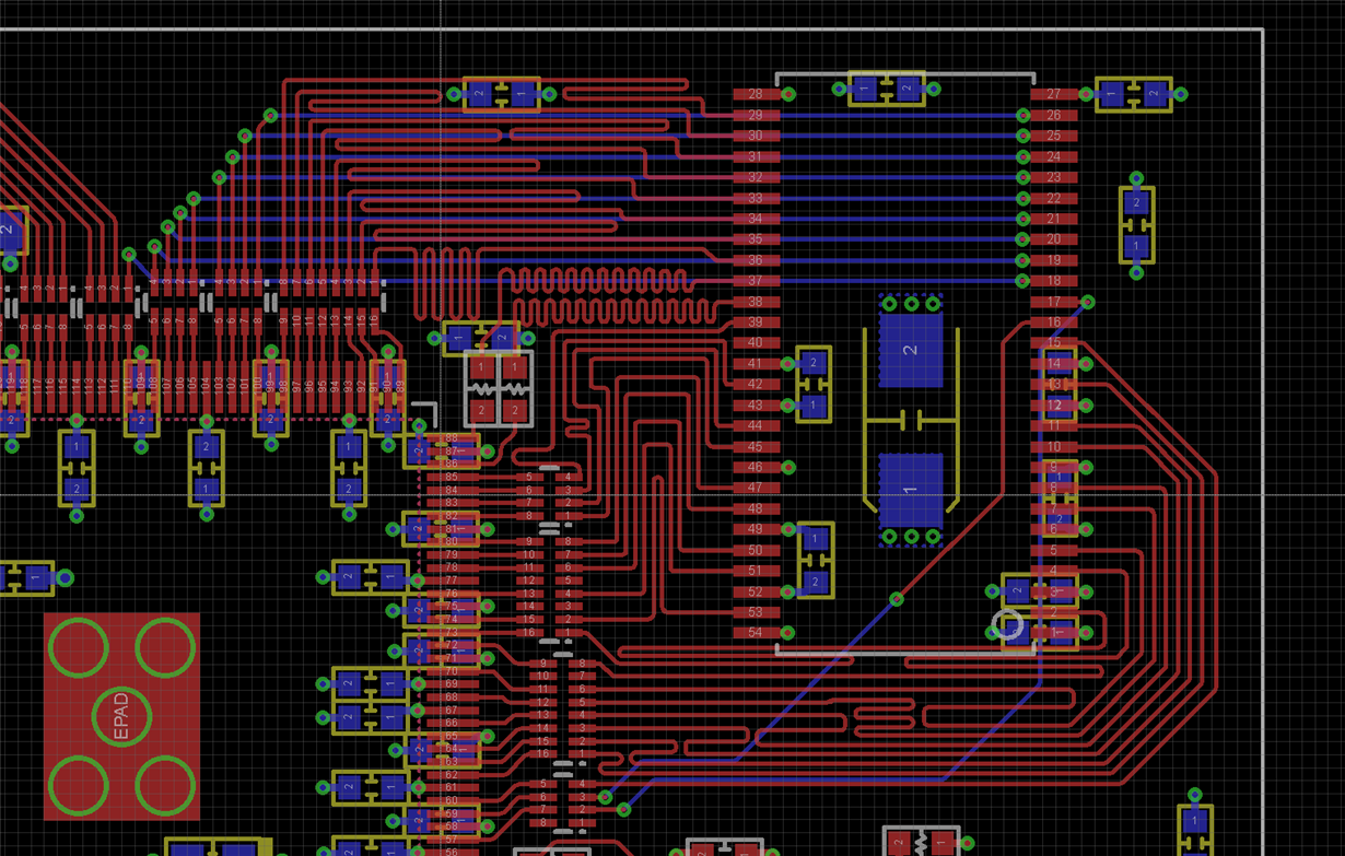
C6745 PCB SDRAM Layout

Using an SMD SDRAM on EMIFB, I have a feeling I blew the layout.

I matched all control signals within 0.5mm, DQM0/D0-7 within 0.2mm, DQM1/D8-15 within 0.2mm

But, the references I could find did not emphasize any relation between these three groups of signals, just match within the group.

CAS/RAS/CS0/A0-A12/BA0-BA1 = 37mm +/- 0.5mm

DQM0/D0-D7 17.5mm +/- 0.2mm

DQM1/D8-D15 42.5 +/- 0.2mm

WE/CKE/CLK 30mm +/- 0.5mm

1 x IS42S16800F-7TL SDRAM @128MHz/Latency=2

When I run, only the lower 8-bits gets read back from the SDRAM. The scope shows all lines with clean signal forms, though my setup is hard to do for multiple lines at once.

I ran the speed down to 60MHz and the same occurs.

  • Stuart,

    There is no PCB routing guideline available for SDRAM interface in specific from TI. I recommend you to perform simulations to confirm that your design meet the timing requirements.

    Please ensure that you configured the SDRAM correctly ?

    Regards,
    Senthil
  • How about in general?  This is not "new" tech, but the amount of info I can find is very limited.  I do not have an IBIS simulator, so it is kinda hard to simulate.

  • Stuart,

    Here is the SDRAM routing guidelines for 16 bit interface that i got over the internet. Please check if you meet them.

    Rule 1: match Data[7:0], DQM0 to within 0.3 inches of each other.
    Rule 2: match Data[15:8], DQM1 to within 0.3 inches of each other.
    Rule 3: match signal groups from rule 1 and rule 2 to within 1.0 inches of each other.
    Rule 4: match CLK to within +/-0.30 inches of signal groups rule 1 and rule 2.
    Rule 5: match A[14:0], BA[1:0], RAS, CAS, CS_N, WR_N, CKE to within +- 0.500 inches of CLK.

    Regards,
    Senthil
  • I'm within those rules, and after a fourth look at the actual board, it seems the resistor pack on DQM1 had the pad contact cold-soldered.

    We re-soldered and now data is coming through, but with occasional errors. I will try adjusting timing parameters to see if it solves them.

    I am using 33ohm resistor nets right against the pins of the 6745 as termination. Is that a good value? I matched the traces to 50ohm.

    Regards,

    Stuart.

  • Stuart,

    Good progress. In general, 33 ohms series resistance is the best value. However simulation is required to identify the right value to minimize the reflections.

    Regards,
    Senthil