This thread has been locked.

If you have a related question, please click the "Ask a related question" button in the top right corner. The newly created question will be automatically linked to this question.

[K2H EVM] Boot failure with SOC_POWER_GOOD

Other Parts Discussed in Thread: UCD9244, UCD9090

Hi,

My customer just bought a K2H evm and got stuck with EVM boot failure.

Here is a BMC log.

BMC VERSION 1.0.2.6
BUILT Nov  5 2013 13:06:10
---------------------

[00:00:00]  BMC Init Begin
[00:00:00]  BMC Version 1.0.2.6
[00:00:00]  XTCIEVMK2X
[00:00:00]  4.0
[00:00:00]  S/N: 109481
[00:00:00]  BMC Init Complete
[00:00:00]  Main PWR Start Begin
[00:00:00]  Main PWR Start Complete
[00:00:00]  SOC PWR Start Begin
[00:00:00]  EVM setup has encountered the following error: The signal SOC_POWER_GOOD has failed to assert
[00:00:00]  SOC PWR Stop Begin
[00:00:01]  SOC PWR Stop Complete
[00:00:01]  HWDBG is set to ON, evm setup will now halt.
[00:00:01]  To alter this behavior, please use the hwdbg command.
BMC>

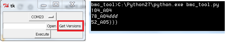
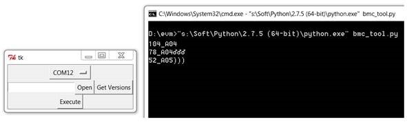
I suggested the customer to upgrade UCD9xxx firmware to the latest version , but unfortunately the problem was still there -- UCD9xxx devices have been upgraded with   UCD9090_104_A03.txt, UCD9244_78_A04.txt and UCD9244_52_A04.txt which these are available from http://www2.advantech.com/Support/TI-EVM/EVMK2HX_sd4.aspx

Is this known issue ? What can we do for this issue ? Can we issue RMA for this EVM ?

Best Regards,
Naoki

  • Naoki-san,

    Yes, it is a known issue.  We have been working with the manufacturer to publish the solution on their website.  Since your customer is already familiar with the process of loading new UCD configuration files, I will provide the draft files that should resolve the problem.  I have tested with the XML project files and validated success.  Once the manufacturer completes their testing, these files will be loaded on their website.

    Tom

    EVM v4_0 patch files draft FEB2016.zip

  • Hello Tom,

    Thank you for your suggestion, but unfortunately, it did not help.
    The problem is still existing after upgrading the UCD device with yours.

    Here is a log :

    BMC VERSION 1.0.2.6
    BUILT Nov 5 2013 13:06:10
    ---------------------

    [00:00:00] BMC Init Begin
    [00:00:00] BMC Version 1.0.2.6
    [00:00:00] XTCIEVMK2X
    [00:00:00] 4.0
    [00:00:00] S/N: 109481
    [00:00:00] BMC Init Complete
    [00:00:00] Main PWR Start Begin
    [00:00:00] Main PWR Start Complete
    [00:00:00] SOC PWR Start Begin
    [00:00:00] EVM setup has encountered the following error: The signal
    SOC_POWER_GOOD has failed to assert
    [00:00:00] SOC PWR Stop Begin
    [00:00:01] SOC PWR Stop Complete
    [00:00:01] HWDBG is set to ON, evm setup will now halt.
    [00:00:01] To alter this behavior, please use the hwdbg command.
    BMC>

    The versions of UCD now look like the following:
    - UCD9090_104_A04
    - UCD9244_78_A04
    - UCD9244_52_A05

    If you don't have further suggestions, we will initiate RMA for this EVM.

    Best Regards,
    Naoki
  • Naoki-san,

    The symptoms have not changed.  I am trying to understand if this is the same issue or a different issue.  I have a few questions:

    1. Did you load both files or just the UCD9244_52_A05?  If not, do you see a change in behavior by loading the UCD9090 configuration?

    2.  If you repeat the power cycle a few times, does it ever successfully boot (try about 5 times)?

    3.  Can you put the files from the web site back into the unit and then retest?  Does a repeated start ever succeed (try about 5 times)?

    Tom

  • Hi Tom,

    Thank you for your reply.
    I'm asking your questions of 1 and 2 to my customer and waiting for the response. In the meanwhile, I reply on your query of 3, with some background:

    The EVM Rev4.0 had been shipped with the following configurations:
    - UCD9090_104_A03
    - UCD9244 _78_A03_02
    - UCD9244_52_A03_03
    With these configurations, they have not succeeded the booting correctly. When they confirmed BMC log, it showed SOC_POWER_GOOD error state.

    And when confirming the latest versions in advantec web site, it appeared the following was the current latest versions for UCD configurations for Rev4.0 EVM:
    - UCD9090_104_A03.txt
    - UCD9244_78_A04.txt
    - UCD9244_52_A04.txt

    We understood UCD9244 was required to update with UCD9244_78_A04.txt and UCD9244_52_A04.txt.
    So the configurations are now looked like the following:
    - UCD9090_104_A03.txt
    - UCD9244_78_A04.txt
    - UCD9244_52_A04.txt

    As you see, the above configurations are the current latest versions, but still they saw the issue.
    Of cause, they have tried over 5 times, but no success.
    And because of that, I asked e2e, and got your suggestions, but no success, unfortunately.

    Best Regards,
    Naoki
  • Naoki Kawada said:
    I'm asking your questions of 1 and 2 to my customer and waiting for the response.

    I got some feedback from the customer. UCD9090_104_A04_TI_30%_20151120.txt has been applied, but no success.

    Here is the current status:

    - UCD9090_104_A04_TI_30%_20151120.txt 
    UCD9244_78_A04.txt
    UCD9244_52_A04.txt

    Best Regards,
    Naoki


  • We have updated UCD files to fix power issue. We recommend you to go through the known issue document and fix the power issue by updating the UCDs.

    Please take a look at know issue document and download UCD files from below link.

    http://www2.advantech.com/Support/TI-EVM/EVMK2HX_sd4.aspx

    Thank you.

  • Hi Raja,

    Thank you for your notification.
    Unfortunately, we had already initiated the replacement process for the EVM.
    We can't try your suggestion now.
    I'll try it if we saw the same error on other EVMs/Customers.

    Best Regards,
    Naoki
  • Hi Raja,

    I got a new EVM for the replacement. I need to check if this new EVM works correctly before shipping it to my customer. Unfortunately, I confirmed the new EVM sometimes did not work with the same problem... So now I tried your uploaded UCD files. But still,I sometimes saw the same error.

    Here are updated UCD files I used for this EVM:

    # Format=Tab; Hex=CompactUpper; BreakOutBytes=True; PEC=True [DO NOT REMOVE THIS LINE IF YOU WANT TO IMPORT USING A FUSION TOOL]
    # PEC byte is calculated on all message bytes, including addresses and Read/Write bit.
    # For reads, the last field is what is expected back from the device
    # Creator: Texas Instruments Fusion Digital Power Designer v1.8.325
    # Date: 2014?10?8?
    # Write PHASE_INFO [MFR 02] Rail #1: 1 Phase: 1A; Rail #2: 1 Phase: 2A; Rail #3: 1 Phase: 3A; Rail #4: 1 Phase: 4A
    I2CWrite	9C	D2	04	01	04	10	40	32
    # Write FREQUENCY_SWITCH [Rail #1] 751.0 kHz
    I2CWrite	9C	00	00	53
    I2CWrite	9C	33	EF	02	6C
    # Write FREQUENCY_SWITCH [Rail #2] 751.0 kHz
    I2CWrite	9C	00	01	54
    I2CWrite	9C	33	EF	02	6C
    # Write FREQUENCY_SWITCH [Rail #3] 751.0 kHz
    I2CWrite	9C	00	02	5D
    I2CWrite	9C	33	EF	02	6C
    # Write FREQUENCY_SWITCH [Rail #4] 751.0 kHz
    I2CWrite	9C	00	03	5A
    I2CWrite	9C	33	EF	02	6C
    # Execute STORE_DEFAULT_ALL
    I2CWrite	9C	11	6A
    Pause	1000	Pausing 1,000.00 ms for STORE_DEFAULT_ALL hold time
    # Execute SOFT_RESET [MFR 11]
    I2CWrite	9C	DB	12
    Pause	2000	Pausing 2,000.00 ms for Reset device and wait for it to come back online
    # Write VID_CONFIG [Rail #1] Format: Ignore, Vout Low: 0.000V, Vout High: 0.000V, Lockout Interval: 0 msec
    I2CWrite	9C	00	00	53
    I2CWrite	9C	BB	09	00	00	00	00	00	00	00	00	00	5F
    # Write VID_CONFIG [Rail #2] Format: Ignore, Vout Low: 0.000V, Vout High: 0.000V, Lockout Interval: 0 msec
    I2CWrite	9C	00	01	54
    I2CWrite	9C	BB	09	00	00	00	00	00	00	00	00	00	5F
    # Write VID_CONFIG [Rail #3] Format: Ignore, Vout Low: 0.000V, Vout High: 0.000V, Lockout Interval: 0 msec
    I2CWrite	9C	00	02	5D
    I2CWrite	9C	BB	09	00	00	00	00	00	00	00	00	00	5F
    # Write VID_CONFIG [Rail #4] Format: Ignore, Vout Low: 0.000V, Vout High: 0.000V, Lockout Interval: 0 msec
    I2CWrite	9C	00	03	5A
    I2CWrite	9C	BB	09	00	00	00	00	00	00	00	00	00	5F
    # Write MFR_DATE 130506
    I2CWrite	9C	9D	06	31	33	30	35	30	36	9F
    # Write MFR_ID MFR_ID
    I2CWrite	9C	99	06	4D	46	52	5F	49	44	E5
    # Write MFR_LOCATION TAIWAN
    I2CWrite	9C	9C	06	54	41	49	57	41	4E	49
    # Write MFR_MODEL DSPM-8305E
    I2CWrite	9C	9A	0A	44	53	50	4D	2D	38	33	30	35	45	CC
    # Write MFR_REVISION 78_A04
    I2CWrite	9C	9B	06	37	38	5F	41	30	34	F9
    # Write MFR_SERIAL 000000
    I2CWrite	9C	9E	06	30	30	30	30	30	30	F7
    # Write SECURITY_BIT_MASK [MFR 36] No commands write protected
    I2CWrite	9C	F4	20	00	00	00	00	00	00	00	00	00	00	00	00	00	00	00	00	00	00	00	00	00	00	00	00	00	00	00	00	00	00	00	00	C5
    # Write SYNC_CONFIG Sync Output Source: None; Rail #1: Trigger Source=None, Delay=0%; Rail #2: Trigger Source=DPWM1, Delay=25%; Rail #3: Trigger Source=DPWM2, Delay=25%; Rail #4: Trigger Source=DPWM3, Delay=25%
    I2CWrite	9C	B9	09	00	00	00	01	40	02	40	03	40	D2
    # Write USER_DATA_00 User_Data_00
    I2CWrite	9C	B0	0C	55	73	65	72	5F	44	61	74	61	5F	30	30	5A
    # Write VIN_OFF 5.000 V
    I2CWrite	9C	36	80	CA	EC
    # Write VIN_ON 6.000 V
    I2CWrite	9C	35	00	CB	E0
    # Write VIN_OV_FAULT_LIMIT 16.500 V
    I2CWrite	9C	55	10	DA	05
    # Write VIN_OV_FAULT_RESPONSE Response=2,Restart=0,Delay=0
    I2CWrite	9C	56	80	A8
    # Write VIN_OV_WARN_LIMIT 15.000 V
    I2CWrite	9C	57	C0	D3	56
    # Write VIN_SCALE [MFR 03] 0.130 
    I2CWrite	9C	D3	14	A2	48
    # Write VIN_UV_FAULT_LIMIT 0.000 V
    I2CWrite	9C	59	00	80	29
    # Write VIN_UV_FAULT_RESPONSE Response=0,Restart=0,Delay=0
    I2CWrite	9C	5A	00	DD
    # Write VIN_UV_WARN_LIMIT 7.797 V
    I2CWrite	9C	58	E6	CB	89
    # Write VOUT_MAX [Rail #1] 1.600 V
    I2CWrite	9C	00	00	53
    I2CWrite	9C	24	99	19	45
    # Write ON_OFF_CONFIG [Rail #1] Mode: CONTROL Pin Only; Control: Active High, Use TOFF_DELAY/TOFF_FALL
    I2CWrite	9C	02	16	1B
    # Write CLA_GAINS_BANK_0 [META,Rail #1] B1=[2.65234 -4.54297 1.92578] A1=[1.00000 -1.22656 0.22656] B2=[1.00000 0.00000] A2=[1.00000 0.00000] AFE_Gain=4 Limits=[-5.00,-4.00,3.00,4.00] Gains=[1.00,1.00,1.00,1.00,1.00]
    I2CWrite	9C	D4	00	BD
    I2CWrite	9C	D5	18	02	A7	0B	75	01	ED	00	03	01	3A	0F	C6	00	00	00	00	84	10	41	04	04	03	3C	3B	15
    # Write CLA_GAINS_BANK_1 [META,Rail #1] B1=[2.65234 -4.54297 1.92578] A1=[1.00000 -1.22656 0.22656] B2=[1.00000 0.00000] A2=[1.00000 0.00000] AFE_Gain=4 Limits=[-5.00,-4.00,3.00,4.00] Gains=[2.00,1.75,1.00,1.75,2.00]
    I2CWrite	9C	D4	01	BA
    I2CWrite	9C	D5	18	02	A7	0B	75	01	ED	00	03	01	3A	0F	C6	00	00	00	00	84	1C	81	C8	04	03	3C	3B	D9
    # Write CLA_GAINS_BANK_2 [META,Rail #1] B1=[0.00000 0.00000 0.00000] A1=[1.00000 -1.00000 0.00000] B2=[1.00000 0.00000] A2=[1.00000 0.00000] AFE_Gain=1 Limits=[-5.00,-3.00,3.00,5.00] Gains=[1.00,1.00,1.00,1.00,1.00]
    I2CWrite	9C	D4	02	B3
    I2CWrite	9C	D5	18	00	00	00	00	00	00	00	03	01	00	00	00	00	00	00	00	04	10	41	04	05	03	3D	3B	07
    # Write DRIVER_CONFIG [MFR 06,Rail #1] DPWM Shutdown Action: TriState, Fault Pin On Restart Mode: IgnoreFaultPin, Interrupt Pin Polarity: ActiveHigh
    I2CWrite	9C	D6	01	90
    # Write DRIVER_MIN_PULSE [MFR 15,Rail #1] 30 ns
    I2CWrite	9C	DF	C0	DB	34
    # Write EADC_SAMPLE_TRIGGER [MFR 07,Rail #1] 228 ns
    I2CWrite	9C	D7	90	F3	B1
    # Write FAST_OC_FAULT_LIMIT [MFR 39,Rail #1] 37.50 A/Phase
    I2CWrite	9C	F7	58	E2	C0
    # Write IOUT_OC_FAULT_LIMIT [Rail #1] 32.50 A
    I2CWrite	9C	46	08	E2	4D
    # Write IOUT_OC_FAULT_RESPONSE [Rail #1] Response=2,Restart=0,Delay=0
    I2CWrite	9C	47	80	EA
    # Write IOUT_OC_LV_FAULT_LIMIT [Rail #1] 0.870 V
    I2CWrite	9C	48	EB	0D	9E
    # Write IOUT_OC_LV_FAULT_RESPONSE [Rail #1] Response=2,Restart=0,Delay=0
    I2CWrite	9C	49	80	3C
    # Write IOUT_OC_WARN_LIMIT [Rail #1] 26.25 A
    I2CWrite	9C	4A	48	DB	43
    # Write IOUT_UC_FAULT_LIMIT [Rail #1] -8.25 A
    I2CWrite	9C	4B	F0	D5	E5
    # Write IOUT_UC_FAULT_RESPONSE [Rail #1] Response=0,Restart=0,Delay=0
    I2CWrite	9C	4C	00	F4
    # Write LIGHT_LOAD_CONFIG [MFR 29,Rail #1] CLA Gain Control: NormalLoad; Phase Control: NormalLoad; Num Light Load Phases: 1
    I2CWrite	9C	ED	00	F9
    # Write LIGHT_LOAD_LIMIT_HIGH [MFR 27,Rail #1] 0.00 A
    I2CWrite	9C	EB	00	80	15
    # Write LIGHT_LOAD_LIMIT_LOW [MFR 38,Rail #1] 0.00 A
    I2CWrite	9C	F6	00	80	26
    # Write MAX_DUTY [Rail #1] 99.0 %
    I2CWrite	9C	32	18	EB	E9
    # Write OT_FAULT_LIMIT [Rail #1] 150 C
    I2CWrite	9C	4F	58	F2	0B
    # Write OT_FAULT_RESPONSE [Rail #1] Response=0,Restart=0,Delay=0
    I2CWrite	9C	50	00	5F
    # Write OT_WARN_LIMIT [Rail #1] 100 C
    I2CWrite	9C	51	20	EB	C0
    # Write PHASE_DROP_CAL [MFR 42,Rail #1] 1.000 
    I2CWrite	9C	FA	00	BA	7A
    # Write POWER_GOOD_OFF [Rail #1] 0.850 V
    I2CWrite	9C	5F	99	0D	A2
    # Write POWER_GOOD_ON [Rail #1] 0.900 V
    I2CWrite	9C	5E	66	0E	17
    # Write SMBALERT_MASK_CML [Rail #1] <EMPTY>
    I2CWrite	9C	1B	7E	00	84
    # Write SMBALERT_MASK_INPUT [Rail #1] <EMPTY>
    I2CWrite	9C	1B	7C	00	AE
    # Write SMBALERT_MASK_IOUT [Rail #1] <EMPTY>
    I2CWrite	9C	1B	7B	00	C5
    # Write SMBALERT_MASK_MFR_SPECIFIC [Rail #1] <EMPTY>
    I2CWrite	9C	1B	80	00	46
    # Write SMBALERT_MASK_OTHER [Rail #1] <EMPTY>
    I2CWrite	9C	1B	7F	00	91
    # Write SMBALERT_MASK_TEMPERATURE [Rail #1] <EMPTY>
    I2CWrite	9C	1B	7D	00	BB
    # Write SMBALERT_MASK_VOUT [Rail #1] VOUT_OV_FAULT
    I2CWrite	9C	1B	7A	80	59
    # Write THERMAL_COEFF [MFR 13,Rail #1] 0.394 %/C
    I2CWrite	9C	DD	27	AB	9D
    # Write TOFF_DELAY [Rail #1] 0.0 ms
    I2CWrite	9C	64	00	80	59
    # Write TOFF_FALL [Rail #1] 4.0 ms
    I2CWrite	9C	65	FF	C3	2B
    # Write TOFF_MAX_WARN_LIMIT [Rail #1] <No Limit>
    I2CWrite	9C	66	00	80	8F
    # Write TON_DELAY [Rail #1] 0.0 ms
    I2CWrite	9C	60	00	80	F2
    # Write TON_MAX_FAULT_LIMIT [Rail #1] 20.0 ms
    I2CWrite	9C	62	80	DA	13
    # Write TON_MAX_FAULT_RESPONSE [Rail #1] Response=0,Restart=0,Delay=0
    I2CWrite	9C	63	00	99
    # Write TON_RISE [Rail #1] 4.0 ms
    I2CWrite	9C	61	FF	C3	80
    # Write TRACKING_MODE [MFR 22,Rail #1] Off
    I2CWrite	9C	E6	FF	9D
    # Write TRACKING_SCALE_MONITOR [MFR 23,Rail #1] 1.000 
    I2CWrite	9C	E7	00	BA	49
    # Write VOUT_CAL_MONITOR [MFR 01,Rail #1] 0.000 V
    I2CWrite	9C	D1	00	00	FA
    # Write VOUT_CAL_OFFSET [Rail #1] 0.000 V
    I2CWrite	9C	23	00	00	40
    # Write VOUT_COMMAND [Rail #1] 1.000 V
    I2CWrite	9C	21	00	10	E6
    # Write VOUT_MARGIN_HIGH [Rail #1] 1.050 V
    I2CWrite	9C	25	CC	10	5C
    # Write VOUT_MARGIN_LOW [Rail #1] 0.950 V
    I2CWrite	9C	26	33	0F	6B
    # Write VOUT_OV_FAULT_LIMIT [Rail #1] 1.150 V
    I2CWrite	9C	40	66	12	CD
    # Write VOUT_OV_FAULT_RESPONSE [Rail #1] Response=2,Restart=0,Delay=0
    I2CWrite	9C	41	80	94
    # Write VOUT_OV_WARN_LIMIT [Rail #1] 1.100 V
    I2CWrite	9C	42	99	11	C5
    # Write VOUT_SCALE_LOOP [Rail #1] 1.000 
    I2CWrite	9C	29	00	BA	E8
    # Write VOUT_SCALE_MONITOR [Rail #1] 1.000 
    I2CWrite	9C	2A	00	BA	55
    # Write VOUT_TRANSITION_RATE [Rail #1] 0.250 mV/us
    I2CWrite	9C	27	01	AA	A1
    # Write VOUT_UV_FAULT_LIMIT [Rail #1] 0.850 V
    I2CWrite	9C	44	99	0D	EC
    # Write VOUT_UV_FAULT_RESPONSE [Rail #1] Response=0,Restart=0,Delay=0
    I2CWrite	9C	45	00	49
    # Write VOUT_UV_WARN_LIMIT [Rail #1] 0.900 V
    I2CWrite	9C	43	66	0E	24
    # Write IOUT_CAL_GAIN_1 [Rail #1] 69.88 mohm
    I2CWrite	9C	38	2F	EA	FB
    # Write IOUT_CAL_OFFSET_1 [Rail #1] -4.30 A
    I2CWrite	9C	39	DA	CD	30
    # Write TEMPERATURE_CAL_GAIN_1 [MFR 20,Rail #1] 100.0 C/V
    I2CWrite	9C	E4	20	EB	EA
    # Write TEMPERATURE_CAL_OFFSET_1 [MFR 21,Rail #1] -47.00 C
    I2CWrite	9C	E5	10	E5	52
    # Write VOUT_MAX [Rail #2] 1.600 V
    I2CWrite	9C	00	01	54
    I2CWrite	9C	24	99	19	45
    # Write ON_OFF_CONFIG [Rail #2] Mode: CONTROL Pin Only; Control: Active High, Use TOFF_DELAY/TOFF_FALL
    I2CWrite	9C	02	16	1B
    # Write CLA_GAINS_BANK_0 [META,Rail #2] B1=[6.08594 -11.50000 5.43750] A1=[1.00000 -1.22656 0.22656] B2=[1.00000 0.00000] A2=[1.00000 0.00000] AFE_Gain=4 Limits=[-5.00,-4.00,3.00,4.00] Gains=[1.00,1.00,1.00,1.00,1.00]
    I2CWrite	9C	D4	00	BD
    I2CWrite	9C	D5	18	03	0B	0A	40	02	B8	00	04	00	9D	0F	E3	00	00	00	00	84	10	41	04	04	03	3C	3B	19
    # Write CLA_GAINS_BANK_1 [META,Rail #2] B1=[6.08594 -11.50000 5.43750] A1=[1.00000 -1.22656 0.22656] B2=[1.00000 0.00000] A2=[1.00000 0.00000] AFE_Gain=4 Limits=[-5.00,-4.00,3.00,4.00] Gains=[2.00,1.75,1.00,1.75,2.00]
    I2CWrite	9C	D4	01	BA
    I2CWrite	9C	D5	18	03	0B	0A	40	02	B8	00	04	00	9D	0F	E3	00	00	00	00	84	1C	81	C8	04	03	3C	3B	D5
    # Write CLA_GAINS_BANK_2 [META,Rail #2] B1=[0.00000 0.00000 0.00000] A1=[1.00000 -1.00000 0.00000] B2=[1.00000 0.00000] A2=[1.00000 0.00000] AFE_Gain=1 Limits=[-5.00,-3.00,3.00,5.00] Gains=[1.00,1.00,1.00,1.00,1.00]
    I2CWrite	9C	D4	02	B3
    I2CWrite	9C	D5	18	00	00	00	00	00	00	00	03	01	00	00	00	00	00	00	00	04	10	41	04	05	03	3D	3B	07
    # Write DRIVER_CONFIG [MFR 06,Rail #2] DPWM Shutdown Action: TriState, Fault Pin On Restart Mode: IgnoreFaultPin, Interrupt Pin Polarity: ActiveHigh
    I2CWrite	9C	D6	01	90
    # Write DRIVER_MIN_PULSE [MFR 15,Rail #2] 30 ns
    I2CWrite	9C	DF	C0	DB	34
    # Write EADC_SAMPLE_TRIGGER [MFR 07,Rail #2] 228 ns
    I2CWrite	9C	D7	90	F3	B1
    # Write FAST_OC_FAULT_LIMIT [MFR 39,Rail #2] 37.50 A/Phase
    I2CWrite	9C	F7	58	E2	C0
    # Write IOUT_OC_FAULT_LIMIT [Rail #2] 32.50 A
    I2CWrite	9C	46	08	E2	4D
    # Write IOUT_OC_FAULT_RESPONSE [Rail #2] Response=2,Restart=0,Delay=0
    I2CWrite	9C	47	80	EA
    # Write IOUT_OC_LV_FAULT_LIMIT [Rail #2] 0.870 V
    I2CWrite	9C	48	EB	0D	9E
    # Write IOUT_OC_LV_FAULT_RESPONSE [Rail #2] Response=2,Restart=0,Delay=0
    I2CWrite	9C	49	80	3C
    # Write IOUT_OC_WARN_LIMIT [Rail #2] 26.25 A
    I2CWrite	9C	4A	48	DB	43
    # Write IOUT_UC_FAULT_LIMIT [Rail #2] -8.25 A
    I2CWrite	9C	4B	F0	D5	E5
    # Write IOUT_UC_FAULT_RESPONSE [Rail #2] Response=0,Restart=0,Delay=0
    I2CWrite	9C	4C	00	F4
    # Write LIGHT_LOAD_CONFIG [MFR 29,Rail #2] CLA Gain Control: NormalLoad; Phase Control: NormalLoad; Num Light Load Phases: 1
    I2CWrite	9C	ED	00	F9
    # Write LIGHT_LOAD_LIMIT_HIGH [MFR 27,Rail #2] 0.00 A
    I2CWrite	9C	EB	00	80	15
    # Write LIGHT_LOAD_LIMIT_LOW [MFR 38,Rail #2] 0.00 A
    I2CWrite	9C	F6	00	80	26
    # Write MAX_DUTY [Rail #2] 99.0 %
    I2CWrite	9C	32	18	EB	E9
    # Write OT_FAULT_LIMIT [Rail #2] 150 C
    I2CWrite	9C	4F	58	F2	0B
    # Write OT_FAULT_RESPONSE [Rail #2] Response=2,Restart=0,Delay=0
    I2CWrite	9C	50	80	D6
    # Write OT_WARN_LIMIT [Rail #2] 100 C
    I2CWrite	9C	51	20	EB	C0
    # Write PHASE_DROP_CAL [MFR 42,Rail #2] 1.000 
    I2CWrite	9C	FA	00	BA	7A
    # Write POWER_GOOD_OFF [Rail #2] 0.850 V
    I2CWrite	9C	5F	99	0D	A2
    # Write POWER_GOOD_ON [Rail #2] 0.900 V
    I2CWrite	9C	5E	66	0E	17
    # Write SMBALERT_MASK_CML [Rail #2] <EMPTY>
    I2CWrite	9C	1B	7E	00	84
    # Write SMBALERT_MASK_INPUT [Rail #2] <EMPTY>
    I2CWrite	9C	1B	7C	00	AE
    # Write SMBALERT_MASK_IOUT [Rail #2] <EMPTY>
    I2CWrite	9C	1B	7B	00	C5
    # Write SMBALERT_MASK_MFR_SPECIFIC [Rail #2] <EMPTY>
    I2CWrite	9C	1B	80	00	46
    # Write SMBALERT_MASK_OTHER [Rail #2] <EMPTY>
    I2CWrite	9C	1B	7F	00	91
    # Write SMBALERT_MASK_TEMPERATURE [Rail #2] OT_FAULT
    I2CWrite	9C	1B	7D	80	32
    # Write SMBALERT_MASK_VOUT [Rail #2] VOUT_OV_FAULT
    I2CWrite	9C	1B	7A	80	59
    # Write THERMAL_COEFF [MFR 13,Rail #2] 0.394 %/C
    I2CWrite	9C	DD	27	AB	9D
    # Write TOFF_DELAY [Rail #2] 0.0 ms
    I2CWrite	9C	64	00	80	59
    # Write TOFF_FALL [Rail #2] 4.0 ms
    I2CWrite	9C	65	FF	C3	2B
    # Write TOFF_MAX_WARN_LIMIT [Rail #2] <No Limit>
    I2CWrite	9C	66	00	80	8F
    # Write TON_DELAY [Rail #2] 0.0 ms
    I2CWrite	9C	60	00	80	F2
    # Write TON_MAX_FAULT_LIMIT [Rail #2] 20.0 ms
    I2CWrite	9C	62	80	DA	13
    # Write TON_MAX_FAULT_RESPONSE [Rail #2] Response=0,Restart=0,Delay=0
    I2CWrite	9C	63	00	99
    # Write TON_RISE [Rail #2] 4.0 ms
    I2CWrite	9C	61	FF	C3	80
    # Write TRACKING_MODE [MFR 22,Rail #2] Off
    I2CWrite	9C	E6	80	E7
    # Write TRACKING_SCALE_MONITOR [MFR 23,Rail #2] 1.000 
    I2CWrite	9C	E7	00	BA	49
    # Write VOUT_CAL_MONITOR [MFR 01,Rail #2] 0.000 V
    I2CWrite	9C	D1	00	00	FA
    # Write VOUT_CAL_OFFSET [Rail #2] 0.000 V
    I2CWrite	9C	23	00	00	40
    # Write VOUT_COMMAND [Rail #2] 1.000 V
    I2CWrite	9C	21	00	10	E6
    # Write VOUT_MARGIN_HIGH [Rail #2] 1.050 V
    I2CWrite	9C	25	CC	10	5C
    # Write VOUT_MARGIN_LOW [Rail #2] 0.950 V
    I2CWrite	9C	26	33	0F	6B
    # Write VOUT_OV_FAULT_LIMIT [Rail #2] 1.150 V
    I2CWrite	9C	40	66	12	CD
    # Write VOUT_OV_FAULT_RESPONSE [Rail #2] Response=2,Restart=0,Delay=0
    I2CWrite	9C	41	80	94
    # Write VOUT_OV_WARN_LIMIT [Rail #2] 1.100 V
    I2CWrite	9C	42	99	11	C5
    # Write VOUT_SCALE_LOOP [Rail #2] 1.000 
    I2CWrite	9C	29	00	BA	E8
    # Write VOUT_SCALE_MONITOR [Rail #2] 1.000 
    I2CWrite	9C	2A	00	BA	55
    # Write VOUT_TRANSITION_RATE [Rail #2] 0.250 mV/us
    I2CWrite	9C	27	01	AA	A1
    # Write VOUT_UV_FAULT_LIMIT [Rail #2] 0.850 V
    I2CWrite	9C	44	99	0D	EC
    # Write VOUT_UV_FAULT_RESPONSE [Rail #2] Response=0,Restart=0,Delay=0
    I2CWrite	9C	45	00	49
    # Write VOUT_UV_WARN_LIMIT [Rail #2] 0.900 V
    I2CWrite	9C	43	66	0E	24
    # Write IOUT_CAL_GAIN_1 [Rail #2] 88.13 mohm
    I2CWrite	9C	38	C1	EA	6E
    # Write IOUT_CAL_OFFSET_1 [Rail #2] -4.50 A
    I2CWrite	9C	39	C0	CD	E5
    # Write TEMPERATURE_CAL_GAIN_1 [MFR 20,Rail #2] 100.0 C/V
    I2CWrite	9C	E4	20	EB	EA
    # Write TEMPERATURE_CAL_OFFSET_1 [MFR 21,Rail #2] -47.00 C
    I2CWrite	9C	E5	10	E5	52
    # Write VOUT_MAX [Rail #3] 1.600 V
    I2CWrite	9C	00	02	5D
    I2CWrite	9C	24	99	19	45
    # Write ON_OFF_CONFIG [Rail #3] Mode: CONTROL Pin Only; Control: Active High, Use TOFF_DELAY/TOFF_FALL
    I2CWrite	9C	02	16	1B
    # Write CLA_GAINS_BANK_0 [META,Rail #3] B1=[2.85938 -4.65625 1.83984] A1=[1.00000 -1.22656 0.22656] B2=[1.00000 0.00000] A2=[1.00000 0.00000] AFE_Gain=4 Limits=[-5.00,-4.00,3.00,4.00] Gains=[1.00,1.00,1.00,1.00,1.00]
    I2CWrite	9C	D4	00	BD
    I2CWrite	9C	D5	18	02	DC	0B	58	01	D7	00	03	01	3A	0F	C6	00	00	00	00	84	10	41	04	04	03	3C	3B	8F
    # Write CLA_GAINS_BANK_1 [META,Rail #3] B1=[2.85938 -4.65625 1.83984] A1=[1.00000 -1.22656 0.22656] B2=[1.00000 0.00000] A2=[1.00000 0.00000] AFE_Gain=4 Limits=[-5.00,-4.00,3.00,4.00] Gains=[2.00,1.75,1.00,1.75,2.00]
    I2CWrite	9C	D4	01	BA
    I2CWrite	9C	D5	18	02	DC	0B	58	01	D7	00	03	01	3A	0F	C6	00	00	00	00	84	1C	81	C8	04	03	3C	3B	43
    # Write CLA_GAINS_BANK_2 [META,Rail #3] B1=[0.00000 0.00000 0.00000] A1=[1.00000 -1.00000 0.00000] B2=[1.00000 0.00000] A2=[1.00000 0.00000] AFE_Gain=1 Limits=[-5.00,-3.00,3.00,5.00] Gains=[1.00,1.00,1.00,1.00,1.00]
    I2CWrite	9C	D4	02	B3
    I2CWrite	9C	D5	18	00	00	00	00	00	00	00	03	01	00	00	00	00	00	00	00	04	10	41	04	05	03	3D	3B	07
    # Write DRIVER_CONFIG [MFR 06,Rail #3] DPWM Shutdown Action: TriState, Fault Pin On Restart Mode: IgnoreFaultPin, Interrupt Pin Polarity: ActiveHigh
    I2CWrite	9C	D6	01	90
    # Write DRIVER_MIN_PULSE [MFR 15,Rail #3] 20 ns
    I2CWrite	9C	DF	80	DA	68
    # Write EADC_SAMPLE_TRIGGER [MFR 07,Rail #3] 228 ns
    I2CWrite	9C	D7	90	F3	B1
    # Write FAST_OC_FAULT_LIMIT [MFR 39,Rail #3] 6.00 A/Phase
    I2CWrite	9C	F7	00	CB	BB
    # Write IOUT_OC_FAULT_LIMIT [Rail #3] 5.20 A
    I2CWrite	9C	46	9A	CA	5E
    # Write IOUT_OC_FAULT_RESPONSE [Rail #3] Response=2,Restart=0,Delay=0
    I2CWrite	9C	47	80	EA
    # Write IOUT_OC_LV_FAULT_LIMIT [Rail #3] 0.826 V
    I2CWrite	9C	48	39	0D	0E
    # Write IOUT_OC_LV_FAULT_RESPONSE [Rail #3] Response=2,Restart=0,Delay=0
    I2CWrite	9C	49	80	3C
    # Write IOUT_OC_WARN_LIMIT [Rail #3] 4.20 A
    I2CWrite	9C	4A	1A	CA	12
    # Write IOUT_UC_FAULT_LIMIT [Rail #3] -1.31 A
    I2CWrite	9C	4B	60	BD	1B
    # Write IOUT_UC_FAULT_RESPONSE [Rail #3] Response=0,Restart=0,Delay=0
    I2CWrite	9C	4C	00	F4
    # Write LIGHT_LOAD_CONFIG [MFR 29,Rail #3] CLA Gain Control: NormalLoad; Phase Control: NormalLoad; Num Light Load Phases: 1
    I2CWrite	9C	ED	00	F9
    # Write LIGHT_LOAD_LIMIT_HIGH [MFR 27,Rail #3] 0.00 A
    I2CWrite	9C	EB	00	80	15
    # Write LIGHT_LOAD_LIMIT_LOW [MFR 38,Rail #3] 0.00 A
    I2CWrite	9C	F6	00	80	26
    # Write MAX_DUTY [Rail #3] 99.0 %
    I2CWrite	9C	32	18	EB	E9
    # Write OT_FAULT_LIMIT [Rail #3] 150 C
    I2CWrite	9C	4F	58	F2	0B
    # Write OT_FAULT_RESPONSE [Rail #3] Response=2,Restart=0,Delay=0
    I2CWrite	9C	50	80	D6
    # Write OT_WARN_LIMIT [Rail #3] 100 C
    I2CWrite	9C	51	20	EB	C0
    # Write PHASE_DROP_CAL [MFR 42,Rail #3] 1.000 
    I2CWrite	9C	FA	00	BA	7A
    # Write POWER_GOOD_OFF [Rail #3] 0.807 V
    I2CWrite	9C	5F	EB	0C	2D
    # Write POWER_GOOD_ON [Rail #3] 0.855 V
    I2CWrite	9C	5E	AE	0D	5B
    # Write SMBALERT_MASK_CML [Rail #3] <EMPTY>
    I2CWrite	9C	1B	7E	00	84
    # Write SMBALERT_MASK_INPUT [Rail #3] <EMPTY>
    I2CWrite	9C	1B	7C	00	AE
    # Write SMBALERT_MASK_IOUT [Rail #3] <EMPTY>
    I2CWrite	9C	1B	7B	00	C5
    # Write SMBALERT_MASK_MFR_SPECIFIC [Rail #3] <EMPTY>
    I2CWrite	9C	1B	80	00	46
    # Write SMBALERT_MASK_OTHER [Rail #3] <EMPTY>
    I2CWrite	9C	1B	7F	00	91
    # Write SMBALERT_MASK_TEMPERATURE [Rail #3] OT_FAULT
    I2CWrite	9C	1B	7D	80	32
    # Write SMBALERT_MASK_VOUT [Rail #3] VOUT_OV_FAULT
    I2CWrite	9C	1B	7A	80	59
    # Write THERMAL_COEFF [MFR 13,Rail #3] 0.000 %/C
    I2CWrite	9C	DD	00	80	89
    # Write TOFF_DELAY [Rail #3] 0.0 ms
    I2CWrite	9C	64	00	80	59
    # Write TOFF_FALL [Rail #3] 3.8 ms
    I2CWrite	9C	65	CC	C3	ED
    # Write TOFF_MAX_WARN_LIMIT [Rail #3] <No Limit>
    I2CWrite	9C	66	00	80	8F
    # Write TON_DELAY [Rail #3] 10.0 ms
    I2CWrite	9C	60	80	D2	FD
    # Write TON_MAX_FAULT_LIMIT [Rail #3] 19.0 ms
    I2CWrite	9C	62	60	DA	50
    # Write TON_MAX_FAULT_RESPONSE [Rail #3] Response=0,Restart=0,Delay=0
    I2CWrite	9C	63	00	99
    # Write TON_RISE [Rail #3] 3.8 ms
    I2CWrite	9C	61	CC	C3	46
    # Write TRACKING_MODE [MFR 22,Rail #3] Off
    I2CWrite	9C	E6	80	E7
    # Write TRACKING_SCALE_MONITOR [MFR 23,Rail #3] 1.000 
    I2CWrite	9C	E7	00	BA	49
    # Write VOUT_CAL_MONITOR [MFR 01,Rail #3] 0.000 V
    I2CWrite	9C	D1	00	00	FA
    # Write VOUT_CAL_OFFSET [Rail #3] 0.000 V
    I2CWrite	9C	23	00	00	40
    # Write VOUT_COMMAND [Rail #3] 0.950 V
    I2CWrite	9C	21	33	0F	7D
    # Write VOUT_MARGIN_HIGH [Rail #3] 0.997 V
    I2CWrite	9C	25	F5	0F	45
    # Write VOUT_MARGIN_LOW [Rail #3] 0.902 V
    I2CWrite	9C	26	70	0E	08
    # Write VOUT_OV_FAULT_LIMIT [Rail #3] 1.092 V
    I2CWrite	9C	40	7A	11	6F
    # Write VOUT_OV_FAULT_RESPONSE [Rail #3] Response=2,Restart=0,Delay=0
    I2CWrite	9C	41	80	94
    # Write VOUT_OV_WARN_LIMIT [Rail #3] 1.045 V
    I2CWrite	9C	42	B8	10	79
    # Write VOUT_SCALE_LOOP [Rail #3] 1.000 
    I2CWrite	9C	29	00	BA	E8
    # Write VOUT_SCALE_MONITOR [Rail #3] 1.000 
    I2CWrite	9C	2A	00	BA	55
    # Write VOUT_TRANSITION_RATE [Rail #3] 0.250 mV/us
    I2CWrite	9C	27	01	AA	A1
    # Write VOUT_UV_FAULT_LIMIT [Rail #3] 0.807 V
    I2CWrite	9C	44	EB	0C	63
    # Write VOUT_UV_FAULT_RESPONSE [Rail #3] Response=0,Restart=0,Delay=0
    I2CWrite	9C	45	00	49
    # Write VOUT_UV_WARN_LIMIT [Rail #3] 0.855 V
    I2CWrite	9C	43	AE	0D	68
    # Write IOUT_CAL_GAIN_1 [Rail #3] 139.75 mohm
    I2CWrite	9C	38	2F	F2	B3
    # Write IOUT_CAL_OFFSET_1 [Rail #3] 0.00 A
    I2CWrite	9C	39	00	80	EC
    # Write TEMPERATURE_CAL_GAIN_1 [MFR 20,Rail #3] 100.0 C/V
    I2CWrite	9C	E4	20	EB	EA
    # Write TEMPERATURE_CAL_OFFSET_1 [MFR 21,Rail #3] -47.00 C
    I2CWrite	9C	E5	10	E5	52
    # Write VOUT_MAX [Rail #4] 1.600 V
    I2CWrite	9C	00	03	5A
    I2CWrite	9C	24	99	19	45
    # Write ON_OFF_CONFIG [Rail #4] Mode: CONTROL Pin Only; Control: Active High, Use TOFF_DELAY/TOFF_FALL
    I2CWrite	9C	02	16	1B
    # Write CLA_GAINS_BANK_0 [META,Rail #4] B1=[2.85938 -4.65625 1.83984] A1=[1.00000 -1.22656 0.22656] B2=[1.00000 0.00000] A2=[1.00000 0.00000] AFE_Gain=4 Limits=[-5.00,-4.00,3.00,4.00] Gains=[1.00,1.00,1.00,1.00,1.00]
    I2CWrite	9C	D4	00	BD
    I2CWrite	9C	D5	18	02	DC	0B	58	01	D7	00	03	01	3A	0F	C6	00	00	00	00	84	10	41	04	04	03	3C	3B	8F
    # Write CLA_GAINS_BANK_1 [META,Rail #4] B1=[2.85938 -4.65625 1.83984] A1=[1.00000 -1.22656 0.22656] B2=[1.00000 0.00000] A2=[1.00000 0.00000] AFE_Gain=4 Limits=[-5.00,-4.00,3.00,4.00] Gains=[2.00,1.75,1.00,1.75,2.00]
    I2CWrite	9C	D4	01	BA
    I2CWrite	9C	D5	18	02	DC	0B	58	01	D7	00	03	01	3A	0F	C6	00	00	00	00	84	1C	81	C8	04	03	3C	3B	43
    # Write CLA_GAINS_BANK_2 [META,Rail #4] B1=[0.00000 0.00000 0.00000] A1=[1.00000 -1.00000 0.00000] B2=[1.00000 0.00000] A2=[1.00000 0.00000] AFE_Gain=1 Limits=[-5.00,-3.00,3.00,5.00] Gains=[1.00,1.00,1.00,1.00,1.00]
    I2CWrite	9C	D4	02	B3
    I2CWrite	9C	D5	18	00	00	00	00	00	00	00	03	01	00	00	00	00	00	00	00	04	10	41	04	05	03	3D	3B	07
    # Write DRIVER_CONFIG [MFR 06,Rail #4] DPWM Shutdown Action: TriState, Fault Pin On Restart Mode: IgnoreFaultPin, Interrupt Pin Polarity: ActiveHigh
    I2CWrite	9C	D6	01	90
    # Write DRIVER_MIN_PULSE [MFR 15,Rail #4] 20 ns
    I2CWrite	9C	DF	80	DA	68
    # Write EADC_SAMPLE_TRIGGER [MFR 07,Rail #4] 228 ns
    I2CWrite	9C	D7	90	F3	B1
    # Write FAST_OC_FAULT_LIMIT [MFR 39,Rail #4] 25.00 A/Phase
    I2CWrite	9C	F7	20	DB	65
    # Write IOUT_OC_FAULT_LIMIT [Rail #4] 6.50 A
    I2CWrite	9C	46	40	CB	61
    # Write IOUT_OC_FAULT_RESPONSE [Rail #4] Response=2,Restart=0,Delay=0
    I2CWrite	9C	47	80	EA
    # Write IOUT_OC_LV_FAULT_LIMIT [Rail #4] 0.826 V
    I2CWrite	9C	48	39	0D	0E
    # Write IOUT_OC_LV_FAULT_RESPONSE [Rail #4] Response=2,Restart=0,Delay=0
    I2CWrite	9C	49	80	3C
    # Write IOUT_OC_WARN_LIMIT [Rail #4] 5.25 A
    I2CWrite	9C	4A	A0	CA	DF
    # Write IOUT_UC_FAULT_LIMIT [Rail #4] -1.66 A
    I2CWrite	9C	4B	B0	BC	A6
    # Write IOUT_UC_FAULT_RESPONSE [Rail #4] Response=0,Restart=0,Delay=0
    I2CWrite	9C	4C	00	F4
    # Write LIGHT_LOAD_CONFIG [MFR 29,Rail #4] CLA Gain Control: NormalLoad; Phase Control: NormalLoad; Num Light Load Phases: 1
    I2CWrite	9C	ED	00	F9
    # Write LIGHT_LOAD_LIMIT_HIGH [MFR 27,Rail #4] 0.00 A
    I2CWrite	9C	EB	00	80	15
    # Write LIGHT_LOAD_LIMIT_LOW [MFR 38,Rail #4] 0.00 A
    I2CWrite	9C	F6	00	80	26
    # Write MAX_DUTY [Rail #4] 99.0 %
    I2CWrite	9C	32	18	EB	E9
    # Write OT_FAULT_LIMIT [Rail #4] 150 C
    I2CWrite	9C	4F	58	F2	0B
    # Write OT_FAULT_RESPONSE [Rail #4] Response=2,Restart=0,Delay=0
    I2CWrite	9C	50	80	D6
    # Write OT_WARN_LIMIT [Rail #4] 100 C
    I2CWrite	9C	51	20	EB	C0
    # Write PHASE_DROP_CAL [MFR 42,Rail #4] 1.000 
    I2CWrite	9C	FA	00	BA	7A
    # Write POWER_GOOD_OFF [Rail #4] 0.807 V
    I2CWrite	9C	5F	EB	0C	2D
    # Write POWER_GOOD_ON [Rail #4] 0.855 V
    I2CWrite	9C	5E	AE	0D	5B
    # Write SMBALERT_MASK_CML [Rail #4] <EMPTY>
    I2CWrite	9C	1B	7E	00	84
    # Write SMBALERT_MASK_INPUT [Rail #4] <EMPTY>
    I2CWrite	9C	1B	7C	00	AE
    # Write SMBALERT_MASK_IOUT [Rail #4] <EMPTY>
    I2CWrite	9C	1B	7B	00	C5
    # Write SMBALERT_MASK_MFR_SPECIFIC [Rail #4] <EMPTY>
    I2CWrite	9C	1B	80	00	46
    # Write SMBALERT_MASK_OTHER [Rail #4] <EMPTY>
    I2CWrite	9C	1B	7F	00	91
    # Write SMBALERT_MASK_TEMPERATURE [Rail #4] <EMPTY>
    I2CWrite	9C	1B	7D	00	BB
    # Write SMBALERT_MASK_VOUT [Rail #4] <EMPTY>
    I2CWrite	9C	1B	7A	00	D0
    # Write THERMAL_COEFF [MFR 13,Rail #4] 0.000 %/C
    I2CWrite	9C	DD	00	80	89
    # Write TOFF_DELAY [Rail #4] 0.0 ms
    I2CWrite	9C	64	00	80	59
    # Write TOFF_FALL [Rail #4] 3.8 ms
    I2CWrite	9C	65	CC	C3	ED
    # Write TOFF_MAX_WARN_LIMIT [Rail #4] <No Limit>
    I2CWrite	9C	66	00	80	8F
    # Write TON_DELAY [Rail #4] 10.0 ms
    I2CWrite	9C	60	80	D2	FD
    # Write TON_MAX_FAULT_LIMIT [Rail #4] 19.0 ms
    I2CWrite	9C	62	60	DA	50
    # Write TON_MAX_FAULT_RESPONSE [Rail #4] Response=0,Restart=0,Delay=0
    I2CWrite	9C	63	00	99
    # Write TON_RISE [Rail #4] 3.8 ms
    I2CWrite	9C	61	CC	C3	46
    # Write TRACKING_MODE [MFR 22,Rail #4] Off
    I2CWrite	9C	E6	80	E7
    # Write TRACKING_SCALE_MONITOR [MFR 23,Rail #4] 1.000 
    I2CWrite	9C	E7	00	BA	49
    # Write VOUT_CAL_MONITOR [MFR 01,Rail #4] 0.000 V
    I2CWrite	9C	D1	00	00	FA
    # Write VOUT_CAL_OFFSET [Rail #4] 0.000 V
    I2CWrite	9C	23	00	00	40
    # Write VOUT_COMMAND [Rail #4] 0.950 V
    I2CWrite	9C	21	33	0F	7D
    # Write VOUT_MARGIN_HIGH [Rail #4] 0.997 V
    I2CWrite	9C	25	F5	0F	45
    # Write VOUT_MARGIN_LOW [Rail #4] 0.902 V
    I2CWrite	9C	26	70	0E	08
    # Write VOUT_OV_FAULT_LIMIT [Rail #4] 1.092 V
    I2CWrite	9C	40	7A	11	6F
    # Write VOUT_OV_FAULT_RESPONSE [Rail #4] Response=2,Restart=0,Delay=0
    I2CWrite	9C	41	80	94
    # Write VOUT_OV_WARN_LIMIT [Rail #4] 1.045 V
    I2CWrite	9C	42	B8	10	79
    # Write VOUT_SCALE_LOOP [Rail #4] 1.000 
    I2CWrite	9C	29	00	BA	E8
    # Write VOUT_SCALE_MONITOR [Rail #4] 1.000 
    I2CWrite	9C	2A	00	BA	55
    # Write VOUT_TRANSITION_RATE [Rail #4] 0.250 mV/us
    I2CWrite	9C	27	01	AA	A1
    # Write VOUT_UV_FAULT_LIMIT [Rail #4] 0.807 V
    I2CWrite	9C	44	EB	0C	63
    # Write VOUT_UV_FAULT_RESPONSE [Rail #4] Response=0,Restart=0,Delay=0
    I2CWrite	9C	45	00	49
    # Write VOUT_UV_WARN_LIMIT [Rail #4] 0.855 V
    I2CWrite	9C	43	AE	0D	68
    # Write IOUT_CAL_GAIN_1 [Rail #4] 129.75 mohm
    I2CWrite	9C	38	07	F2	B5
    # Write IOUT_CAL_OFFSET_1 [Rail #4] 0.00 A
    I2CWrite	9C	39	00	80	EC
    # Write TEMPERATURE_CAL_GAIN_1 [MFR 20,Rail #4] 100.0 C/V
    I2CWrite	9C	E4	20	EB	EA
    # Write TEMPERATURE_CAL_OFFSET_1 [MFR 21,Rail #4] -47.00 C
    I2CWrite	9C	E5	10	E5	52
    # Store configuration to data flash
    # Execute STORE_DEFAULT_ALL
    I2CWrite	9C	11	6A
    Pause	1000	Pausing 1,000.00 ms for STORE_DEFAULT_ALL hold time
    

    # Format=Tab; Hex=CompactUpper; BreakOutBytes=True; PEC=False [DO NOT REMOVE THIS LINE IF YOU WANT TO IMPORT USING A FUSION TOOL]
    # For reads, the last field is what is expected back from the device
    # Creator: Texas Instruments Fusion Digital Power Designer v2.0.50
    # Date: Monday, February 15, 2016
    # Exported from UCD9244 - Firmware: 6.4.0.12746
    # Write PHASE_INFO [MFR 02] Rail #1: 1 Phase: 1A; Rail #2: 1 Phase: 2A; Rail #3: 1 Phase: 3A; Rail #4: 1 Phase: 4A
    I2CWrite	68	D2	04	01	04	10	40
    # Write FREQUENCY_SWITCH [Rail #1] 500.0 kHz
    I2CWrite	68	00	00
    I2CWrite	68	33	E8	FB
    # Write FREQUENCY_SWITCH [Rail #2] 500.0 kHz
    I2CWrite	68	00	01
    I2CWrite	68	33	E8	FB
    # Write FREQUENCY_SWITCH [Rail #3] 500.0 kHz
    I2CWrite	68	00	02
    I2CWrite	68	33	E8	FB
    # Write FREQUENCY_SWITCH [Rail #4] 500.0 kHz
    I2CWrite	68	00	03
    I2CWrite	68	33	E8	FB
    # Execute STORE_DEFAULT_ALL
    I2CWrite	68	11
    Pause	1000	Pausing 1,000.00 ms for STORE_DEFAULT_ALL hold time
    # Execute SOFT_RESET [MFR 11]
    I2CWrite	68	DB
    Pause	2000	Pausing 2,000.00 ms for Reset device and wait for it to come back online
    # Write VID_CONFIG [Rail #1] Format: Ignore, Vout Low: 0.000V, Vout High: 0.000V, Lockout Interval: 0 msec
    I2CWrite	68	00	00
    I2CWrite	68	BB	09	00	00	00	00	00	00	00	00	00
    # Write VID_CONFIG [Rail #2] Format: Ignore, Vout Low: 0.000V, Vout High: 0.000V, Lockout Interval: 0 msec
    I2CWrite	68	00	01
    I2CWrite	68	BB	09	00	00	00	00	00	00	00	00	00
    # Write VID_CONFIG [Rail #3] Format: Ignore, Vout Low: 0.000V, Vout High: 0.000V, Lockout Interval: 0 msec
    I2CWrite	68	00	02
    I2CWrite	68	BB	09	00	00	00	00	00	00	00	00	00
    # Write VID_CONFIG [Rail #4] Format: Ignore, Vout Low: 0.000V, Vout High: 0.000V, Lockout Interval: 0 msec
    I2CWrite	68	00	03
    I2CWrite	68	BB	09	00	00	00	00	00	00	00	00	00
    # Write MFR_DATE 111215
    I2CWrite	68	9D	06	31	31	31	32	31	35
    # Write MFR_ID MFR_ID
    I2CWrite	68	99	06	4D	46	52	5F	49	44
    # Write MFR_LOCATION TAIWAN
    I2CWrite	68	9C	06	54	41	49	57	41	4E
    # Write MFR_MODEL DSPM-8305E
    I2CWrite	68	9A	0A	44	53	50	4D	2D	38	33	30	35	45
    # Write MFR_REVISION 52_A05
    I2CWrite	68	9B	06	35	32	5F	41	30	35
    # Write MFR_SERIAL 000000
    I2CWrite	68	9E	06	30	30	30	30	30	30
    # Write SECURITY_BIT_MASK [MFR 36] No commands write protected
    I2CWrite	68	F4	20	00	00	00	00	00	00	00	00	00	00	00	00	00	00	00	00	00	00	00	00	00	00	00	00	00	00	00	00	00	00	00	00
    # Write SYNC_CONFIG Sync Output Source: None; Rail #1: Trigger Source=None, Delay=0%; Rail #2: Trigger Source=DPWM1, Delay=25%; Rail #3: Trigger Source=DPWM2, Delay=25%; Rail #4: Trigger Source=DPWM3, Delay=25%
    I2CWrite	68	B9	09	00	00	00	01	40	02	40	03	40
    # Write USER_DATA_00 User_Data_00
    I2CWrite	68	B0	0C	55	73	65	72	5F	44	61	74	61	5F	30	30
    # Write VIN_OFF 5.000 V
    I2CWrite	68	36	80	CA
    # Write VIN_ON 6.000 V
    I2CWrite	68	35	00	CB
    # Write VIN_OV_FAULT_LIMIT 14.297 V
    I2CWrite	68	55	93	D3
    # Write VIN_OV_FAULT_RESPONSE Response=2,Restart=0,Delay=0
    I2CWrite	68	56	80
    # Write VIN_OV_WARN_LIMIT 13.000 V
    I2CWrite	68	57	40	D3
    # Write VIN_SCALE [MFR 03] 0.131 
    I2CWrite	68	D3	19	A2
    # Write VIN_UV_FAULT_LIMIT 0.000 V
    I2CWrite	68	59	00	80
    # Write VIN_UV_FAULT_RESPONSE Response=0,Restart=0,Delay=0
    I2CWrite	68	5A	00
    # Write VIN_UV_WARN_LIMIT 7.797 V
    I2CWrite	68	58	E6	CB
    # Write VOUT_MAX [Rail #1] 1.900 V
    I2CWrite	68	00	00
    I2CWrite	68	24	66	1E
    # Write ON_OFF_CONFIG [Rail #1] Mode: CONTROL Pin Only; Control: Active High, Use TOFF_DELAY/TOFF_FALL
    I2CWrite	68	02	16
    # Write CLA_GAINS_BANK_0 [META,Rail #1] B1=[1.98242 -3.37109 1.40820] A1=[1.00000 -1.22852 0.22852] B2=[1.00000 0.00000] A2=[1.00000 0.00000] AFE_Gain=4 Limits=[-5.00,-4.00,3.00,4.00] Gains=[1.00,1.00,1.00,1.00,1.00]
    I2CWrite	68	D4	00
    I2CWrite	68	D5	18	03	F7	09	42	02	D1	00	02	02	75	0F	8B	00	00	00	00	84	10	41	04	04	03	3C	3B
    # Write CLA_GAINS_BANK_1 [META,Rail #1] B1=[1.98242 -3.37109 1.40820] A1=[1.00000 -1.22852 0.22852] B2=[1.00000 0.00000] A2=[1.00000 0.00000] AFE_Gain=4 Limits=[-5.00,-4.00,3.00,4.00] Gains=[2.00,1.75,1.00,1.75,2.00]
    I2CWrite	68	D4	01
    I2CWrite	68	D5	18	03	F7	09	42	02	D1	00	02	02	75	0F	8B	00	00	00	00	84	1C	81	C8	04	03	3C	3B
    # Write CLA_GAINS_BANK_2 [META,Rail #1] B1=[0.00000 0.00000 0.00000] A1=[1.00000 -1.00000 0.00000] B2=[1.00000 0.00000] A2=[1.00000 0.00000] AFE_Gain=1 Limits=[-5.00,-3.00,3.00,5.00] Gains=[1.00,1.00,1.00,1.00,1.00]
    I2CWrite	68	D4	02
    I2CWrite	68	D5	18	00	00	00	00	00	00	00	03	01	00	00	00	00	00	00	00	04	10	41	04	05	03	3D	3B
    # Write DRIVER_CONFIG [MFR 06,Rail #1] DPWM Shutdown Action: TriState, Fault Pin On Restart Mode: IgnoreFaultPin, Interrupt Pin Polarity: ActiveHigh
    I2CWrite	68	D6	01
    # Write DRIVER_MIN_PULSE [MFR 15,Rail #1] 20 ns
    I2CWrite	68	DF	80	DA
    # Write EADC_SAMPLE_TRIGGER [MFR 07,Rail #1] 224 ns
    I2CWrite	68	D7	80	F3
    # Write FAST_OC_FAULT_LIMIT [MFR 39,Rail #1] 9.000 A/Phase
    I2CWrite	68	F7	40	D2
    # Write IOUT_OC_FAULT_LIMIT [Rail #1] 7.797 A
    I2CWrite	68	46	E6	CB
    # Write IOUT_OC_FAULT_RESPONSE [Rail #1] Response=2,Restart=0,Delay=0
    I2CWrite	68	47	80
    # Write IOUT_OC_LV_FAULT_LIMIT [Rail #1] 1.305 V
    I2CWrite	68	48	E1	14
    # Write IOUT_OC_LV_FAULT_RESPONSE [Rail #1] Response=2,Restart=0,Delay=0
    I2CWrite	68	49	80
    # Write IOUT_OC_WARN_LIMIT [Rail #1] 6.297 A
    I2CWrite	68	4A	26	CB
    # Write IOUT_UC_FAULT_LIMIT [Rail #1] -1.984 A
    I2CWrite	68	4B	08	BC
    # Write IOUT_UC_FAULT_RESPONSE [Rail #1] Response=0,Restart=0,Delay=0
    I2CWrite	68	4C	00
    # Write LIGHT_LOAD_CONFIG [MFR 29,Rail #1] CLA Gain Control: NormalLoad; Phase Control: NormalLoad; Num Light Load Phases: 1
    I2CWrite	68	ED	00
    # Write LIGHT_LOAD_LIMIT_HIGH [MFR 27,Rail #1] 0.000 A
    I2CWrite	68	EB	00	80
    # Write LIGHT_LOAD_LIMIT_LOW [MFR 38,Rail #1] 0.000 A
    I2CWrite	68	F6	00	80
    # Write MAX_DUTY [Rail #1] 99.0 %
    I2CWrite	68	32	18	EB
    # Write OT_FAULT_LIMIT [Rail #1] 150 C
    I2CWrite	68	4F	58	F2
    # Write OT_FAULT_RESPONSE [Rail #1] Response=0,Restart=0,Delay=0
    I2CWrite	68	50	00
    # Write OT_WARN_LIMIT [Rail #1] 100 C
    I2CWrite	68	51	20	EB
    # Write PHASE_DROP_CAL [MFR 42,Rail #1] 1.000 
    I2CWrite	68	FA	00	BA
    # Write POWER_GOOD_OFF [Rail #1] 1.753 V
    I2CWrite	68	5F	0C	1C
    # Write POWER_GOOD_ON [Rail #1] 1.800 V
    I2CWrite	68	5E	CC	1C
    # Write SMBALERT_MASK_CML [Rail #1] <EMPTY>
    I2CWrite	68	1B	7E	00
    # Write SMBALERT_MASK_INPUT [Rail #1] <EMPTY>
    I2CWrite	68	1B	7C	00
    # Write SMBALERT_MASK_IOUT [Rail #1] <EMPTY>
    I2CWrite	68	1B	7B	00
    # Write SMBALERT_MASK_MFR_SPECIFIC [Rail #1] <EMPTY>
    I2CWrite	68	1B	80	00
    # Write SMBALERT_MASK_OTHER [Rail #1] <EMPTY>
    I2CWrite	68	1B	7F	00
    # Write SMBALERT_MASK_TEMPERATURE [Rail #1] <EMPTY>
    I2CWrite	68	1B	7D	00
    # Write SMBALERT_MASK_VOUT [Rail #1] <EMPTY>
    I2CWrite	68	1B	7A	00
    # Write THERMAL_COEFF [MFR 13,Rail #1] 0.394 %/C
    I2CWrite	68	DD	27	AB
    # Write TOFF_DELAY [Rail #1] 0.0 ms
    I2CWrite	68	64	00	80
    # Write TOFF_FALL [Rail #1] 6.0 ms
    I2CWrite	68	65	00	CB
    # Write TOFF_MAX_WARN_LIMIT [Rail #1] <No Limit>
    I2CWrite	68	66	00	80
    # Write TON_DELAY [Rail #1] 0.0 ms
    I2CWrite	68	60	00	80
    # Write TON_MAX_FAULT_LIMIT [Rail #1] <No Limit>
    I2CWrite	68	62	00	80
    # Write TON_MAX_FAULT_RESPONSE [Rail #1] Response=0,Restart=0,Delay=0
    I2CWrite	68	63	00
    # Write TON_RISE [Rail #1] 6.0 ms
    I2CWrite	68	61	00	CB
    # Write TRACKING_MODE [MFR 22,Rail #1] Off
    I2CWrite	68	E6	FF
    # Write TRACKING_SCALE_MONITOR [MFR 23,Rail #1] 1.000 
    I2CWrite	68	E7	00	BA
    # Write VOUT_CAL_MONITOR [MFR 01,Rail #1] -0.030 V
    I2CWrite	68	D1	86	FF
    # Write VOUT_CAL_OFFSET [Rail #1] 0.030 V
    I2CWrite	68	23	7A	00
    # Write VOUT_COMMAND [Rail #1] 1.800 V
    I2CWrite	68	21	CC	1C
    # Write VOUT_MARGIN_HIGH [Rail #1] 1.823 V
    I2CWrite	68	25	2B	1D
    # Write VOUT_MARGIN_LOW [Rail #1] 1.782 V
    I2CWrite	68	26	83	1C
    # Write VOUT_OV_FAULT_LIMIT [Rail #1] 2.340 V
    I2CWrite	68	40	70	25
    # Write VOUT_OV_FAULT_RESPONSE [Rail #1] Response=0,Restart=0,Delay=0
    I2CWrite	68	41	00
    # Write VOUT_OV_WARN_LIMIT [Rail #1] 1.841 V
    I2CWrite	68	42	74	1D
    # Write VOUT_SCALE_LOOP [Rail #1] 0.800 
    I2CWrite	68	29	33	B3
    # Write VOUT_SCALE_MONITOR [Rail #1] 0.800 
    I2CWrite	68	2A	33	B3
    # Write VOUT_TRANSITION_RATE [Rail #1] 0.282 mV/us
    I2CWrite	68	27	42	AA
    # Write VOUT_UV_FAULT_LIMIT [Rail #1] 1.600 V
    I2CWrite	68	44	99	19
    # Write VOUT_UV_FAULT_RESPONSE [Rail #1] Response=0,Restart=0,Delay=0
    I2CWrite	68	45	00
    # Write VOUT_UV_WARN_LIMIT [Rail #1] 1.764 V
    I2CWrite	68	43	39	1C
    # Write IOUT_CAL_GAIN_1 [Rail #1] 99.0 mohm
    I2CWrite	68	38	18	EB
    # Write IOUT_CAL_OFFSET_1 [Rail #1] -4.000000 A
    I2CWrite	68	39	00	CE
    # Write TEMPERATURE_CAL_GAIN_1 [MFR 20,Rail #1] 100.0 C/V
    I2CWrite	68	E4	20	EB
    # Write TEMPERATURE_CAL_OFFSET_1 [MFR 21,Rail #1] -50.00 C
    I2CWrite	68	E5	E0	E4
    # Write VOUT_MAX [Rail #2] 1.772 V
    I2CWrite	68	00	01
    I2CWrite	68	24	59	1C
    # Write ON_OFF_CONFIG [Rail #2] Mode: CONTROL Pin Only; Control: Active High, Use TOFF_DELAY/TOFF_FALL
    I2CWrite	68	02	16
    # Write CLA_GAINS_BANK_0 [META,Rail #2] B1=[0.51172 -0.95020 0.44043] A1=[1.00000 -1.22852 0.22852] B2=[1.00000 0.00000] A2=[1.00000 0.00000] AFE_Gain=4 Limits=[-5.00,-4.00,3.00,4.00] Gains=[1.00,1.00,1.00,1.00,1.00]
    I2CWrite	68	D4	00
    I2CWrite	68	D5	18	02	0C	0C	33	01	C3	00	01	04	EA	0F	16	00	00	00	00	84	10	41	04	04	03	3C	3B
    # Write CLA_GAINS_BANK_1 [META,Rail #2] B1=[0.51172 -0.95020 0.44043] A1=[1.00000 -1.22852 0.22852] B2=[1.00000 0.00000] A2=[1.00000 0.00000] AFE_Gain=4 Limits=[-5.00,-4.00,3.00,4.00] Gains=[2.00,1.75,1.00,1.75,2.00]
    I2CWrite	68	D4	01
    I2CWrite	68	D5	18	02	0C	0C	33	01	C3	00	01	04	EA	0F	16	00	00	00	00	84	1C	81	C8	04	03	3C	3B
    # Write CLA_GAINS_BANK_2 [META,Rail #2] B1=[0.00000 0.00000 0.00000] A1=[1.00000 -1.00000 0.00000] B2=[1.00000 0.00000] A2=[1.00000 0.00000] AFE_Gain=1 Limits=[-5.00,-3.00,3.00,5.00] Gains=[1.00,1.00,1.00,1.00,1.00]
    I2CWrite	68	D4	02
    I2CWrite	68	D5	18	00	00	00	00	00	00	00	03	01	00	00	00	00	00	00	00	04	10	41	04	05	03	3D	3B
    # Write DRIVER_CONFIG [MFR 06,Rail #2] DPWM Shutdown Action: TriState, Fault Pin On Restart Mode: IgnoreFaultPin, Interrupt Pin Polarity: ActiveHigh
    I2CWrite	68	D6	01
    # Write DRIVER_MIN_PULSE [MFR 15,Rail #2] 30 ns
    I2CWrite	68	DF	C0	DB
    # Write EADC_SAMPLE_TRIGGER [MFR 07,Rail #2] 224 ns
    I2CWrite	68	D7	80	F3
    # Write FAST_OC_FAULT_LIMIT [MFR 39,Rail #2] 18.750 A/Phase
    I2CWrite	68	F7	58	DA
    # Write IOUT_OC_FAULT_LIMIT [Rail #2] 16.250 A
    I2CWrite	68	46	08	DA
    # Write IOUT_OC_FAULT_RESPONSE [Rail #2] Response=2,Restart=0,Delay=0
    I2CWrite	68	47	80
    # Write IOUT_OC_LV_FAULT_LIMIT [Rail #2] 1.305 V
    I2CWrite	68	48	E1	14
    # Write IOUT_OC_LV_FAULT_RESPONSE [Rail #2] Response=2,Restart=0,Delay=0
    I2CWrite	68	49	80
    # Write IOUT_OC_WARN_LIMIT [Rail #2] 13.125 A
    I2CWrite	68	4A	48	D3
    # Write IOUT_UC_FAULT_LIMIT [Rail #2] -4.125 A
    I2CWrite	68	4B	F0	CD
    # Write IOUT_UC_FAULT_RESPONSE [Rail #2] Response=0,Restart=0,Delay=0
    I2CWrite	68	4C	00
    # Write LIGHT_LOAD_CONFIG [MFR 29,Rail #2] CLA Gain Control: NormalLoad; Phase Control: NormalLoad; Num Light Load Phases: 1
    I2CWrite	68	ED	00
    # Write LIGHT_LOAD_LIMIT_HIGH [MFR 27,Rail #2] 0.000 A
    I2CWrite	68	EB	00	80
    # Write LIGHT_LOAD_LIMIT_LOW [MFR 38,Rail #2] 0.000 A
    I2CWrite	68	F6	00	80
    # Write MAX_DUTY [Rail #2] 99.0 %
    I2CWrite	68	32	18	EB
    # Write OT_FAULT_LIMIT [Rail #2] 150 C
    I2CWrite	68	4F	58	F2
    # Write OT_FAULT_RESPONSE [Rail #2] Response=2,Restart=0,Delay=0
    I2CWrite	68	50	80
    # Write OT_WARN_LIMIT [Rail #2] 100 C
    I2CWrite	68	51	20	EB
    # Write PHASE_DROP_CAL [MFR 42,Rail #2] 1.000 
    I2CWrite	68	FA	00	BA
    # Write POWER_GOOD_OFF [Rail #2] 1.275 V
    I2CWrite	68	5F	66	14
    # Write POWER_GOOD_ON [Rail #2] 1.350 V
    I2CWrite	68	5E	99	15
    # Write SMBALERT_MASK_CML [Rail #2] <EMPTY>
    I2CWrite	68	1B	7E	00
    # Write SMBALERT_MASK_INPUT [Rail #2] <EMPTY>
    I2CWrite	68	1B	7C	00
    # Write SMBALERT_MASK_IOUT [Rail #2] <EMPTY>
    I2CWrite	68	1B	7B	00
    # Write SMBALERT_MASK_MFR_SPECIFIC [Rail #2] <EMPTY>
    I2CWrite	68	1B	80	00
    # Write SMBALERT_MASK_OTHER [Rail #2] <EMPTY>
    I2CWrite	68	1B	7F	00
    # Write SMBALERT_MASK_TEMPERATURE [Rail #2] <EMPTY>
    I2CWrite	68	1B	7D	00
    # Write SMBALERT_MASK_VOUT [Rail #2] <EMPTY>
    I2CWrite	68	1B	7A	00
    # Write THERMAL_COEFF [MFR 13,Rail #2] 0.394 %/C
    I2CWrite	68	DD	27	AB
    # Write TOFF_DELAY [Rail #2] 0.0 ms
    I2CWrite	68	64	00	80
    # Write TOFF_FALL [Rail #2] 6.0 ms
    I2CWrite	68	65	00	CB
    # Write TOFF_MAX_WARN_LIMIT [Rail #2] <No Limit>
    I2CWrite	68	66	00	80
    # Write TON_DELAY [Rail #2] 10.0 ms
    I2CWrite	68	60	80	D2
    # Write TON_MAX_FAULT_LIMIT [Rail #2] 30.0 ms
    I2CWrite	68	62	C0	DB
    # Write TON_MAX_FAULT_RESPONSE [Rail #2] Response=0,Restart=0,Delay=0
    I2CWrite	68	63	00
    # Write TON_RISE [Rail #2] 6.0 ms
    I2CWrite	68	61	00	CB
    # Write TRACKING_MODE [MFR 22,Rail #2] Off
    I2CWrite	68	E6	80
    # Write TRACKING_SCALE_MONITOR [MFR 23,Rail #2] 1.000 
    I2CWrite	68	E7	00	BA
    # Write VOUT_CAL_MONITOR [MFR 01,Rail #2] -0.160 V
    I2CWrite	68	D1	71	FD
    # Write VOUT_CAL_OFFSET [Rail #2] 0.200 V
    I2CWrite	68	23	33	03
    # Write VOUT_COMMAND [Rail #2] 1.500 V
    I2CWrite	68	21	00	18
    # Write VOUT_MARGIN_HIGH [Rail #2] 1.575 V
    I2CWrite	68	25	33	19
    # Write VOUT_MARGIN_LOW [Rail #2] 1.425 V
    I2CWrite	68	26	CC	16
    # Write VOUT_OV_FAULT_LIMIT [Rail #2] 1.725 V
    I2CWrite	68	40	99	1B
    # Write VOUT_OV_FAULT_RESPONSE [Rail #2] Response=2,Restart=0,Delay=0
    I2CWrite	68	41	80
    # Write VOUT_OV_WARN_LIMIT [Rail #2] 1.650 V
    I2CWrite	68	42	66	1A
    # Write VOUT_SCALE_LOOP [Rail #2] 0.903 
    I2CWrite	68	29	9D	B3
    # Write VOUT_SCALE_MONITOR [Rail #2] 0.903 
    I2CWrite	68	2A	9D	B3
    # Write VOUT_TRANSITION_RATE [Rail #2] 0.250 mV/us
    I2CWrite	68	27	00	AA
    # Write VOUT_UV_FAULT_LIMIT [Rail #2] 1.275 V
    I2CWrite	68	44	66	14
    # Write VOUT_UV_FAULT_RESPONSE [Rail #2] Response=0,Restart=0,Delay=0
    I2CWrite	68	45	00
    # Write VOUT_UV_WARN_LIMIT [Rail #2] 1.350 V
    I2CWrite	68	43	99	15
    # Write IOUT_CAL_GAIN_1 [Rail #2] 87.0 mohm
    I2CWrite	68	38	B8	EA
    # Write IOUT_CAL_OFFSET_1 [Rail #2] -4.500000 A
    I2CWrite	68	39	C0	CD
    # Write TEMPERATURE_CAL_GAIN_1 [MFR 20,Rail #2] 100.0 C/V
    I2CWrite	68	E4	20	EB
    # Write TEMPERATURE_CAL_OFFSET_1 [MFR 21,Rail #2] -50.00 C
    I2CWrite	68	E5	E0	E4
    # Write VOUT_MAX [Rail #3] 3.892 V
    I2CWrite	68	00	02
    I2CWrite	68	24	46	3E
    # Write ON_OFF_CONFIG [Rail #3] Mode: CONTROL Pin Only; Control: Active High, Use TOFF_DELAY/TOFF_FALL
    I2CWrite	68	02	16
    # Write CLA_GAINS_BANK_0 [META,Rail #3] B1=[11.62500 -22.45313 10.84375] A1=[1.00000 -1.21875 0.21875] B2=[1.00000 0.00000] A2=[1.00000 0.00000] AFE_Gain=4 Limits=[-5.00,-4.00,3.00,4.00] Gains=[1.00,1.00,1.00,1.00,1.00]
    I2CWrite	68	D4	00
    I2CWrite	68	D5	18	02	E8	0A	63	02	B6	00	05	00	4E	0F	F2	00	00	00	00	84	10	41	04	04	03	3C	3B
    # Write CLA_GAINS_BANK_1 [META,Rail #3] B1=[11.62500 -22.45313 10.84375] A1=[1.00000 -1.21875 0.21875] B2=[1.00000 0.00000] A2=[1.00000 0.00000] AFE_Gain=4 Limits=[-5.00,-4.00,3.00,4.00] Gains=[2.00,1.75,1.00,1.75,2.00]
    I2CWrite	68	D4	01
    I2CWrite	68	D5	18	02	E8	0A	63	02	B6	00	05	00	4E	0F	F2	00	00	00	00	84	1C	81	C8	04	03	3C	3B
    # Write CLA_GAINS_BANK_2 [META,Rail #3] B1=[0.00000 0.00000 0.00000] A1=[1.00000 -1.00000 0.00000] B2=[1.00000 0.00000] A2=[1.00000 0.00000] AFE_Gain=1 Limits=[-5.00,-3.00,3.00,5.00] Gains=[1.00,1.00,1.00,1.00,1.00]
    I2CWrite	68	D4	02
    I2CWrite	68	D5	18	00	00	00	00	00	00	00	03	01	00	00	00	00	00	00	00	04	10	41	04	05	03	3D	3B
    # Write DRIVER_CONFIG [MFR 06,Rail #3] DPWM Shutdown Action: TriState, Fault Pin On Restart Mode: IgnoreFaultPin, Interrupt Pin Polarity: ActiveHigh
    I2CWrite	68	D6	01
    # Write DRIVER_MIN_PULSE [MFR 15,Rail #3] 20 ns
    I2CWrite	68	DF	80	DA
    # Write EADC_SAMPLE_TRIGGER [MFR 07,Rail #3] 224 ns
    I2CWrite	68	D7	80	F3
    # Write FAST_OC_FAULT_LIMIT [MFR 39,Rail #3] 8.000 A/Phase
    I2CWrite	68	F7	00	D2
    # Write IOUT_OC_FAULT_LIMIT [Rail #3] 6.203 A
    I2CWrite	68	46	1A	CB
    # Write IOUT_OC_FAULT_RESPONSE [Rail #3] Response=2,Restart=0,Delay=0
    I2CWrite	68	47	80
    # Write IOUT_OC_LV_FAULT_LIMIT [Rail #3] 2.871 V
    I2CWrite	68	48	EF	2D
    # Write IOUT_OC_LV_FAULT_RESPONSE [Rail #3] Response=2,Restart=0,Delay=0
    I2CWrite	68	49	80
    # Write IOUT_OC_WARN_LIMIT [Rail #3] 5.203 A
    I2CWrite	68	4A	9A	CA
    # Write IOUT_UC_FAULT_LIMIT [Rail #3] -1.313 A
    I2CWrite	68	4B	60	BD
    # Write IOUT_UC_FAULT_RESPONSE [Rail #3] Response=0,Restart=0,Delay=0
    I2CWrite	68	4C	00
    # Write LIGHT_LOAD_CONFIG [MFR 29,Rail #3] CLA Gain Control: NormalLoad; Phase Control: NormalLoad; Num Light Load Phases: 1
    I2CWrite	68	ED	00
    # Write LIGHT_LOAD_LIMIT_HIGH [MFR 27,Rail #3] 0.000 A
    I2CWrite	68	EB	00	80
    # Write LIGHT_LOAD_LIMIT_LOW [MFR 38,Rail #3] 0.000 A
    I2CWrite	68	F6	00	80
    # Write MAX_DUTY [Rail #3] 99.0 %
    I2CWrite	68	32	18	EB
    # Write OT_FAULT_LIMIT [Rail #3] 150 C
    I2CWrite	68	4F	58	F2
    # Write OT_FAULT_RESPONSE [Rail #3] Response=2,Restart=0,Delay=0
    I2CWrite	68	50	80
    # Write OT_WARN_LIMIT [Rail #3] 100 C
    I2CWrite	68	51	20	EB
    # Write PHASE_DROP_CAL [MFR 42,Rail #3] 1.000 
    I2CWrite	68	FA	00	BA
    # Write POWER_GOOD_OFF [Rail #3] 2.950 V
    I2CWrite	68	5F	33	2F
    # Write POWER_GOOD_ON [Rail #3] 3.135 V
    I2CWrite	68	5E	28	32
    # Write SMBALERT_MASK_CML [Rail #3] <EMPTY>
    I2CWrite	68	1B	7E	00
    # Write SMBALERT_MASK_INPUT [Rail #3] <EMPTY>
    I2CWrite	68	1B	7C	00
    # Write SMBALERT_MASK_IOUT [Rail #3] <EMPTY>
    I2CWrite	68	1B	7B	00
    # Write SMBALERT_MASK_MFR_SPECIFIC [Rail #3] <EMPTY>
    I2CWrite	68	1B	80	00
    # Write SMBALERT_MASK_OTHER [Rail #3] <EMPTY>
    I2CWrite	68	1B	7F	00
    # Write SMBALERT_MASK_TEMPERATURE [Rail #3] <EMPTY>
    I2CWrite	68	1B	7D	00
    # Write SMBALERT_MASK_VOUT [Rail #3] <EMPTY>
    I2CWrite	68	1B	7A	00
    # Write THERMAL_COEFF [MFR 13,Rail #3] 0.000 %/C
    I2CWrite	68	DD	00	80
    # Write TOFF_DELAY [Rail #3] 0.0 ms
    I2CWrite	68	64	00	80
    # Write TOFF_FALL [Rail #3] 13.2 ms
    I2CWrite	68	65	4C	D3
    # Write TOFF_MAX_WARN_LIMIT [Rail #3] <No Limit>
    I2CWrite	68	66	00	80
    # Write TON_DELAY [Rail #3] 150.0 ms
    I2CWrite	68	60	58	F2
    # Write TON_MAX_FAULT_LIMIT [Rail #3] <No Limit>
    I2CWrite	68	62	00	80
    # Write TON_MAX_FAULT_RESPONSE [Rail #3] Response=0,Restart=0,Delay=0
    I2CWrite	68	63	00
    # Write TON_RISE [Rail #3] 50.0 ms
    I2CWrite	68	61	20	E3
    # Write TRACKING_MODE [MFR 22,Rail #3] Off
    I2CWrite	68	E6	80
    # Write TRACKING_SCALE_MONITOR [MFR 23,Rail #3] 1.000 
    I2CWrite	68	E7	00	BA
    # Write VOUT_CAL_MONITOR [MFR 01,Rail #3] 1.590 V
    I2CWrite	68	D1	70	19
    # Write VOUT_CAL_OFFSET [Rail #3] 0.080 V
    I2CWrite	68	23	47	01
    # Write VOUT_COMMAND [Rail #3] 3.300 V
    I2CWrite	68	21	CC	34
    # Write VOUT_MARGIN_HIGH [Rail #3] 3.465 V
    I2CWrite	68	25	70	37
    # Write VOUT_MARGIN_LOW [Rail #3] 3.135 V
    I2CWrite	68	26	28	32
    # Write VOUT_OV_FAULT_LIMIT [Rail #3] 4.000 V
    I2CWrite	68	40	00	40
    # Write VOUT_OV_FAULT_RESPONSE [Rail #3] Response=2,Restart=0,Delay=0
    I2CWrite	68	41	80
    # Write VOUT_OV_WARN_LIMIT [Rail #3] 3.630 V
    I2CWrite	68	42	14	3A
    # Write VOUT_SCALE_LOOP [Rail #3] 0.900 
    I2CWrite	68	29	9A	B3
    # Write VOUT_SCALE_MONITOR [Rail #3] 0.900 
    I2CWrite	68	2A	9A	B3
    # Write VOUT_TRANSITION_RATE [Rail #3] 0.114 mV/us
    I2CWrite	68	27	A6	9B
    # Write VOUT_UV_FAULT_LIMIT [Rail #3] 2.640 V
    I2CWrite	68	44	3D	2A
    # Write VOUT_UV_FAULT_RESPONSE [Rail #3] Response=0,Restart=0,Delay=0
    I2CWrite	68	45	00
    # Write VOUT_UV_WARN_LIMIT [Rail #3] 2.970 V
    I2CWrite	68	43	85	2F
    # Write IOUT_CAL_GAIN_1 [Rail #3] 155.0 mohm
    I2CWrite	68	38	6C	F2
    # Write IOUT_CAL_OFFSET_1 [Rail #3] 0.000000 A
    I2CWrite	68	39	00	80
    # Write TEMPERATURE_CAL_GAIN_1 [MFR 20,Rail #3] 100.0 C/V
    I2CWrite	68	E4	20	EB
    # Write TEMPERATURE_CAL_OFFSET_1 [MFR 21,Rail #3] -47.00 C
    I2CWrite	68	E5	10	E5
    # Write VOUT_MAX [Rail #4] 1.600 V
    I2CWrite	68	00	03
    I2CWrite	68	24	99	19
    # Write ON_OFF_CONFIG [Rail #4] Mode: CONTROL Pin Only; Control: Active High, Use TOFF_DELAY/TOFF_FALL
    I2CWrite	68	02	16
    # Write CLA_GAINS_BANK_0 [META,Rail #4] B1=[0.44141 -0.78223 0.34375] A1=[1.00000 -1.22852 0.22852] B2=[1.00000 0.00000] A2=[1.00000 0.00000] AFE_Gain=4 Limits=[-5.00,-4.00,3.00,4.00] Gains=[1.00,1.00,1.00,1.00,1.00]
    I2CWrite	68	D4	00
    I2CWrite	68	D5	18	01	C4	0C	DF	01	60	00	01	04	EA	0F	16	00	00	00	00	84	10	41	04	04	03	3C	3B
    # Write CLA_GAINS_BANK_1 [META,Rail #4] B1=[0.44141 -0.78223 0.34375] A1=[1.00000 -1.22852 0.22852] B2=[1.00000 0.00000] A2=[1.00000 0.00000] AFE_Gain=4 Limits=[-5.00,-4.00,3.00,4.00] Gains=[2.00,1.75,1.00,1.75,2.00]
    I2CWrite	68	D4	01
    I2CWrite	68	D5	18	01	C4	0C	DF	01	60	00	01	04	EA	0F	16	00	00	00	00	84	1C	81	C8	04	03	3C	3B
    # Write CLA_GAINS_BANK_2 [META,Rail #4] B1=[0.00000 0.00000 0.00000] A1=[1.00000 -1.00000 0.00000] B2=[1.00000 0.00000] A2=[1.00000 0.00000] AFE_Gain=1 Limits=[-5.00,-3.00,3.00,5.00] Gains=[1.00,1.00,1.00,1.00,1.00]
    I2CWrite	68	D4	02
    I2CWrite	68	D5	18	00	00	00	00	00	00	00	03	01	00	00	00	00	00	00	00	04	10	41	04	05	03	3D	3B
    # Write DRIVER_CONFIG [MFR 06,Rail #4] DPWM Shutdown Action: TriState, Fault Pin On Restart Mode: IgnoreFaultPin, Interrupt Pin Polarity: ActiveHigh
    I2CWrite	68	D6	01
    # Write DRIVER_MIN_PULSE [MFR 15,Rail #4] 20 ns
    I2CWrite	68	DF	80	DA
    # Write EADC_SAMPLE_TRIGGER [MFR 07,Rail #4] 224 ns
    I2CWrite	68	D7	80	F3
    # Write FAST_OC_FAULT_LIMIT [MFR 39,Rail #4] 12.000 A/Phase
    I2CWrite	68	F7	00	D3
    # Write IOUT_OC_FAULT_LIMIT [Rail #4] 10.406 A
    I2CWrite	68	46	9A	D2
    # Write IOUT_OC_FAULT_RESPONSE [Rail #4] Response=2,Restart=0,Delay=0
    I2CWrite	68	47	80
    # Write IOUT_OC_LV_FAULT_LIMIT [Rail #4] 0.773 V
    I2CWrite	68	48	5E	0C
    # Write IOUT_OC_LV_FAULT_RESPONSE [Rail #4] Response=2,Restart=0,Delay=0
    I2CWrite	68	49	80
    # Write IOUT_OC_WARN_LIMIT [Rail #4] 8.406 A
    I2CWrite	68	4A	1A	D2
    # Write IOUT_UC_FAULT_LIMIT [Rail #4] -2.641 A
    I2CWrite	68	4B	5C	C5
    # Write IOUT_UC_FAULT_RESPONSE [Rail #4] Response=0,Restart=0,Delay=0
    I2CWrite	68	4C	00
    # Write LIGHT_LOAD_CONFIG [MFR 29,Rail #4] CLA Gain Control: NormalLoad; Phase Control: NormalLoad; Num Light Load Phases: 1
    I2CWrite	68	ED	00
    # Write LIGHT_LOAD_LIMIT_HIGH [MFR 27,Rail #4] 0.000 A
    I2CWrite	68	EB	00	80
    # Write LIGHT_LOAD_LIMIT_LOW [MFR 38,Rail #4] 0.000 A
    I2CWrite	68	F6	00	80
    # Write MAX_DUTY [Rail #4] 99.0 %
    I2CWrite	68	32	18	EB
    # Write OT_FAULT_LIMIT [Rail #4] 150 C
    I2CWrite	68	4F	58	F2
    # Write OT_FAULT_RESPONSE [Rail #4] Response=2,Restart=0,Delay=0
    I2CWrite	68	50	80
    # Write OT_WARN_LIMIT [Rail #4] 100 C
    I2CWrite	68	51	20	EB
    # Write PHASE_DROP_CAL [MFR 42,Rail #4] 1.000 
    I2CWrite	68	FA	00	BA
    # Write POWER_GOOD_OFF [Rail #4] 0.756 V
    I2CWrite	68	5F	18	0C
    # Write POWER_GOOD_ON [Rail #4] 0.801 V
    I2CWrite	68	5E	D0	0C
    # Write SMBALERT_MASK_CML [Rail #4] <EMPTY>
    I2CWrite	68	1B	7E	00
    # Write SMBALERT_MASK_INPUT [Rail #4] <EMPTY>
    I2CWrite	68	1B	7C	00
    # Write SMBALERT_MASK_IOUT [Rail #4] <EMPTY>
    I2CWrite	68	1B	7B	00
    # Write SMBALERT_MASK_MFR_SPECIFIC [Rail #4] <EMPTY>
    I2CWrite	68	1B	80	00
    # Write SMBALERT_MASK_OTHER [Rail #4] <EMPTY>
    I2CWrite	68	1B	7F	00
    # Write SMBALERT_MASK_TEMPERATURE [Rail #4] <EMPTY>
    I2CWrite	68	1B	7D	00
    # Write SMBALERT_MASK_VOUT [Rail #4] <EMPTY>
    I2CWrite	68	1B	7A	00
    # Write THERMAL_COEFF [MFR 13,Rail #4] 0.000 %/C
    I2CWrite	68	DD	00	80
    # Write TOFF_DELAY [Rail #4] 0.0 ms
    I2CWrite	68	64	00	80
    # Write TOFF_FALL [Rail #4] 3.4 ms
    I2CWrite	68	65	66	C3
    # Write TOFF_MAX_WARN_LIMIT [Rail #4] <No Limit>
    I2CWrite	68	66	00	80
    # Write TON_DELAY [Rail #4] 50.0 ms
    I2CWrite	68	60	20	E3
    # Write TON_MAX_FAULT_LIMIT [Rail #4] 17.0 ms
    I2CWrite	68	62	20	DA
    # Write TON_MAX_FAULT_RESPONSE [Rail #4] Response=0,Restart=0,Delay=0
    I2CWrite	68	63	00
    # Write TON_RISE [Rail #4] 3.4 ms
    I2CWrite	68	61	66	C3
    # Write TRACKING_MODE [MFR 22,Rail #4] Off
    I2CWrite	68	E6	80
    # Write TRACKING_SCALE_MONITOR [MFR 23,Rail #4] 1.000 
    I2CWrite	68	E7	00	BA
    # Write VOUT_CAL_MONITOR [MFR 01,Rail #4] 0.240 V
    I2CWrite	68	D1	D7	03
    # Write VOUT_CAL_OFFSET [Rail #4] -0.250 V
    I2CWrite	68	23	00	FC
    # Write VOUT_COMMAND [Rail #4] 0.890 V
    I2CWrite	68	21	3D	0E
    # Write VOUT_MARGIN_HIGH [Rail #4] 0.935 V
    I2CWrite	68	25	F5	0E
    # Write VOUT_MARGIN_LOW [Rail #4] 0.846 V
    I2CWrite	68	26	89	0D
    # Write VOUT_OV_FAULT_LIMIT [Rail #4] 1.023 V
    I2CWrite	68	40	5E	10
    # Write VOUT_OV_FAULT_RESPONSE [Rail #4] Response=2,Restart=0,Delay=0
    I2CWrite	68	41	80
    # Write VOUT_OV_WARN_LIMIT [Rail #4] 0.979 V
    I2CWrite	68	42	A9	0F
    # Write VOUT_SCALE_LOOP [Rail #4] 1.000 
    I2CWrite	68	29	00	BA
    # Write VOUT_SCALE_MONITOR [Rail #4] 1.000 
    I2CWrite	68	2A	00	BA
    # Write VOUT_TRANSITION_RATE [Rail #4] 0.250 mV/us
    I2CWrite	68	27	01	AA
    # Write VOUT_UV_FAULT_LIMIT [Rail #4] 0.756 V
    I2CWrite	68	44	18	0C
    # Write VOUT_UV_FAULT_RESPONSE [Rail #4] Response=0,Restart=0,Delay=0
    I2CWrite	68	45	00
    # Write VOUT_UV_WARN_LIMIT [Rail #4] 0.801 V
    I2CWrite	68	43	D0	0C
    # Write IOUT_CAL_GAIN_1 [Rail #4] 145.0 mohm
    I2CWrite	68	38	44	F2
    # Write IOUT_CAL_OFFSET_1 [Rail #4] 0.000000 A
    I2CWrite	68	39	00	80
    # Write TEMPERATURE_CAL_GAIN_1 [MFR 20,Rail #4] 100.0 C/V
    I2CWrite	68	E4	20	EB
    # Write TEMPERATURE_CAL_OFFSET_1 [MFR 21,Rail #4] -47.00 C
    I2CWrite	68	E5	10	E5
    # Store configuration to data flash
    # Execute STORE_DEFAULT_ALL
    I2CWrite	68	11
    Pause	1000	Pausing 1,000.00 ms for STORE_DEFAULT_ALL hold time
    

    # Format=Tab; Hex=CompactUpper; BreakOutBytes=True; PEC=False [DO NOT REMOVE THIS LINE IF YOU WANT TO IMPORT USING A FUSION TOOL]
    # For reads, the last field is what is expected back from the device
    # Creator: Texas Instruments Fusion Digital Power Designer v2.0.50
    # Date: Monday, February 15, 2016
    # Exported from UCD9090 - Firmware: 2.3.5.0
    # Write VOUT_MODE [Rail #1] EXP -12
    # I2CWrite	D0	00	00
    I2CWrite	D0	20	14
    # Write VOUT_MODE [Rail #2] EXP -14
    I2CWrite	D0	00	01
    I2CWrite	D0	20	12
    # Write VOUT_MODE [Rail #3] EXP -13
    I2CWrite	D0	00	02
    I2CWrite	D0	20	13
    # Write VOUT_MODE [Rail #4] EXP -13
    I2CWrite	D0	00	03
    I2CWrite	D0	20	13
    # Write VOUT_MODE [Rail #5] EXP -13
    I2CWrite	D0	00	04
    I2CWrite	D0	20	13
    # Write VOUT_MODE [Rail #6] EXP -14
    I2CWrite	D0	00	05
    I2CWrite	D0	20	12
    # Write VOUT_MODE [Rail #7] EXP -14
    I2CWrite	D0	00	06
    I2CWrite	D0	20	12
    # Write VOUT_MODE [Rail #8] EXP -11
    I2CWrite	D0	00	07
    I2CWrite	D0	20	15
    # Write VOUT_MODE [Rail #9] EXP -13
    I2CWrite	D0	00	08
    I2CWrite	D0	20	13
    # Write VOUT_MODE [Rail #10] EXP 0
    I2CWrite	D0	00	09
    I2CWrite	D0	20	00
    # Write MONITOR_CONFIG [MFR 05] Pin 1 MON1: Rail #4, Type Voltage; Pin 2 MON2: Rail #5, Type Voltage; Pin 38 MON3: Rail #8, Type Voltage, HW Comparator, AVS); Pin 39 MON4: Rail #1, Type Voltage, HW Comparator, AVS); Pin 40 MON5: Rail #3, Type Voltage, HW Comparator, AVS); Pin 41 MON6: Rail #2, Type Voltage, HW Comparator, AVS); Pin 42 MON7: Rail #6, Type Voltage; Pin 45 MON8: Rail #7, Type Voltage; Pin 46 MON9: Rail #9, Type Voltage; Pin 48 MON10: Rail #10, Type Temperature; Pin 37 MON11: Not Assigned
    I2CWrite	D0	D5	0B	23	24	87	80	82	81	25	26	28	49	00
    # Write GPI_CONFIG [MFR 41] Inputs: Pin 22 GPI1_PWM1 ActiveHigh Input,Pin 23 GPI2_PWM2 ActiveHigh Input
    I2CWrite	D0	F9	0D	45	4D	00	00	00	00	00	00	00	00	00	00	00
    # Write SEQ_CONFIG [MFR 38,Rail #1] Rail On Dep: <None> | GPI On Dep: S | Rail Off Dep: Rail #2 | GPI Off Dep: <None> | Fault Dep: <None> | Enable: Pin 7 GPIO4 ActiveHigh ActivelyDrivenOutput; Seq On Timeout: 0 / Wait Indefinitely; Seq Off Timeout: 0 / Wait Indefinitely
    I2CWrite	D0	00	00
    #I2CWrite	D0	F6	0C	96	01	00	00	00	00	00	00	00	02	00	00
    # Write SEQ_CONFIG [MFR 38,Rail #2] Rail On Dep: Rail #1 | GPI On Dep: <None> | Rail Off Dep: Rail #3 | GPI Off Dep: <None> | Fault Dep: <None> | Enable: Pin 21 GPIO14 ActiveHigh ActivelyDrivenOutput; Seq On Timeout: 0 / Wait Indefinitely; Seq Off Timeout: 0 / Wait Indefinitely
    I2CWrite	D0	00	01
    I2CWrite	D0	F6	0C	56	00	00	00	00	00	00	01	00	04	00	00
    # Write SEQ_CONFIG [MFR 38,Rail #3] Rail On Dep: Rail #2 | GPI On Dep: <None> | Rail Off Dep: Rail #4 | GPI Off Dep: <None> | Fault Dep: <None> | Enable: Pin 18 GPIO13 ActiveHigh ActivelyDrivenOutput; Seq On Timeout: 0 / Wait Indefinitely; Seq Off Timeout: 0 / Wait Indefinitely
    I2CWrite	D0	00	02
    I2CWrite	D0	F6	0C	9E	00	00	00	00	00	00	02	00	08	00	00
    # Write SEQ_CONFIG [MFR 38,Rail #4] Rail On Dep: <None> | GPI On Dep: T | Rail Off Dep: Rail #5 | GPI Off Dep: <None> | Fault Dep: <None> | Enable: Unassigned; Seq On Timeout: 0 / Wait Indefinitely; Seq Off Timeout: 0 / Wait Indefinitely
    I2CWrite	D0	00	03
    I2CWrite	D0	F6	0C	00	02	00	00	00	00	00	00	00	10	00	00
    # Write SEQ_CONFIG [MFR 38,Rail #5] Rail On Dep: Rail #4 | GPI On Dep: <None> | Rail Off Dep: Rail #6,7 | GPI Off Dep: <None> | Fault Dep: <None> | Enable: Unassigned; Seq On Timeout: 0 / Wait Indefinitely; Seq Off Timeout: 0 / Wait Indefinitely
    I2CWrite	D0	00	04
    I2CWrite	D0	F6	0C	00	00	00	00	00	00	00	08	00	60	00	00
    # Write SEQ_CONFIG [MFR 38,Rail #6] Rail On Dep: Rail #5 | GPI On Dep: <None> | Rail Off Dep: Rail #9 | GPI Off Dep: <None> | Fault Dep: <None> | Enable: Pin 26 GPIO17 ActiveHigh ActivelyDrivenOutput; Seq On Timeout: 0 / Wait Indefinitely; Seq Off Timeout: 0 / Wait Indefinitely
    I2CWrite	D0	00	05
    I2CWrite	D0	F6	0C	B6	00	00	00	00	00	00	10	01	00	00	00
    # Write SEQ_CONFIG [MFR 38,Rail #7] Rail On Dep: Rail #5 | GPI On Dep: <None> | Rail Off Dep: Rail #8 | GPI Off Dep: <None> | Fault Dep: <None> | Enable: Unassigned; Seq On Timeout: 0 / Wait Indefinitely; Seq Off Timeout: 0 / Wait Indefinitely
    I2CWrite	D0	00	06
    I2CWrite	D0	F6	0C	5C	00	00	00	00	00	00	10	00	80	00	00
    # Write SEQ_CONFIG [MFR 38,Rail #8] Rail On Dep: Rail #6,7 | GPI On Dep: <None> | Rail Off Dep: Rail #9 | GPI Off Dep: <None> | Fault Dep: <None> | Enable: Pin 6 GPIO3 ActiveHigh ActivelyDrivenOutput; Seq On Timeout: 0 / Wait Indefinitely; Seq Off Timeout: 0 / Wait Indefinitely
    I2CWrite	D0	00	07
    I2CWrite	D0	F6	0C	8E	00	00	00	00	00	00	60	01	00	00	00
    # Write SEQ_CONFIG [MFR 38,Rail #9] Rail On Dep: Rail #8 | GPI On Dep: <None> | Rail Off Dep: <None> | GPI Off Dep: <None> | Fault Dep: <None> | Enable: Unassigned; Seq On Timeout: 0 / Wait Indefinitely; Seq Off Timeout: 0 / Wait Indefinitely
    I2CWrite	D0	00	08
    I2CWrite	D0	F6	0C	04	00	00	00	00	00	00	80	00	00	00	00
    # Write SEQ_CONFIG [MFR 38,Rail #10] Rail On Dep: <None> | GPI On Dep: <None> | Rail Off Dep: <None> | GPI Off Dep: <None> | Fault Dep: <None> | Enable: Unassigned; Seq On Timeout: 0 / Wait Indefinitely; Seq Off Timeout: 0 / Wait Indefinitely
    I2CWrite	D0	00	09
    I2CWrite	D0	F6	0C	04	00	00	00	00	00	00	00	00	00	00	00
    # Write GPO_CONFIG_1 [MFR 40] Pin 4 GPIO1 ActiveHigh ActivelyDrivenOutput; INPUT_S ? INPUT_T ? RAIL2 ? RAIL3 [POWER_GOOD]
    I2CWrite	D0	F7	00
    I2CWrite	D0	F8	15	7E	00	05	00	00	00	06	03	00	00	00	00	00	00	00	00	00	00	00	00	00
    # Write GPO_CONFIG_2 [MFR 40] Pin 24 GPIO15 ActiveHigh ActivelyDrivenOutput; INPUT_S ? RAIL2 ? RAIL3 [POWER_GOOD]
    I2CWrite	D0	F7	01
    I2CWrite	D0	F8	15	A6	00	05	00	80	00	06	01	00	00	00	00	00	00	00	00	00	00	00	00	00
    # Write GPO_CONFIG_3 [MFR 40] Pin 5 GPIO2 ActiveHigh ActivelyDrivenOutput; INPUT_S ? INPUT_T ? OUTPUT_X ? OUTPUT_X ? RAIL2 ? RAIL3 ? RAIL4 [POWER_GOOD]
    I2CWrite	D0	F7	02
    I2CWrite	D0	F8	15	86	00	05	00	00	00	0E	03	03	00	00	00	00	00	00	00	00	00	00	00	00
    # Write GPO_CONFIG_4 [MFR 40] Pin 25 GPIO16 ActiveHigh ActivelyDrivenOutput; INPUT_S ? INPUT_T ? OUTPUT_X ? OUTPUT_X ? OUTPUT_X ? RAIL2 ? RAIL3 ? RAIL4 ? RAIL5 ? RAIL6 ? RAIL7 [POWER_GOOD]
    I2CWrite	D0	F7	03
    I2CWrite	D0	F8	15	AE	00	05	00	00	00	7E	03	07	00	00	00	00	00	00	00	00	00	00	00	00
    # Write GPO_CONFIG_5 [MFR 40] Unassigned; No Mask
    I2CWrite	D0	F7	04
    I2CWrite	D0	F8	15	00	00	00	00	00	00	00	00	00	00	00	00	00	00	00	00	00	00	00	00	00
    # Write GPO_CONFIG_6 [MFR 40] Unassigned; No Mask
    I2CWrite	D0	F7	05
    I2CWrite	D0	F8	15	00	00	00	00	00	00	00	00	00	00	00	00	00	00	00	00	00	00	00	00	00
    # Write GPO_CONFIG_7 [MFR 40] Unassigned; No Mask
    I2CWrite	D0	F7	06
    I2CWrite	D0	F8	15	00	00	00	00	00	00	00	00	00	00	00	00	00	00	00	00	00	00	00	00	00
    # Write GPO_CONFIG_8 [MFR 40] Unassigned; No Mask
    I2CWrite	D0	F7	07
    I2CWrite	D0	F8	15	00	00	00	00	00	00	00	00	00	00	00	00	00	00	00	00	00	00	00	00	00
    # Write GPO_CONFIG_9 [MFR 40] Unassigned; No Mask
    I2CWrite	D0	F7	08
    I2CWrite	D0	F8	15	00	00	00	00	00	00	00	00	00	00	00	00	00	00	00	00	00	00	00	00	00
    # Write GPO_CONFIG_10 [MFR 40] Unassigned; No Mask
    I2CWrite	D0	F7	09
    I2CWrite	D0	F8	15	00	00	00	00	00	00	00	00	00	00	00	00	00	00	00	00	00	00	00	00	00
    # Write PWM_CONFIG_0 [MFR 17] Pin_ID = 0; Duty Cycle: 0.0 %; Frequency: 0 Hz; Phase: 0.0 deg
    I2CWrite	D0	E0	00
    I2CWrite	D0	E1	08	88	00	00	00	00	00	80	00
    # Write PWM_CONFIG_1 [MFR 17] Pin_ID = 1; Duty Cycle: 0.0 %; Frequency: 0 Hz; Phase: 0.0 deg
    I2CWrite	D0	E0	01
    I2CWrite	D0	E1	08	88	00	00	00	00	00	80	00
    # Write PWM_CONFIG_2 [MFR 17] Pin_ID = 2; Duty Cycle: 0.0 %; Frequency: 0 Hz; Phase: 0.0 deg
    I2CWrite	D0	E0	02
    I2CWrite	D0	E1	08	88	00	00	00	00	00	80	00
    # Write PWM_CONFIG_3 [MFR 17] Pin_ID = 3; Duty Cycle: 0.0 %; Frequency: 0 Hz; Phase: 0.0 deg
    I2CWrite	D0	E0	03
    I2CWrite	D0	E1	08	88	00	00	00	00	00	80	00
    # Write PWM_CONFIG_4 [MFR 17] Pin_ID = 4; Duty Cycle: 90.0 %; Frequency: 15.26 kHz; Phase: 0.0 deg
    I2CWrite	D0	E0	04
    I2CWrite	D0	E1	08	EA	D0	00	00	3B	9B	80	00
    # Write PWM_CONFIG_5 [MFR 17] Pin_ID = 5; Duty Cycle: 0.0 %; Frequency: 0 Hz; Phase: 0.0 deg
    I2CWrite	D0	E0	05
    I2CWrite	D0	E1	08	88	00	00	00	00	00	80	00
    # Write PWM_CONFIG_6 [MFR 17] Pin_ID = 6; Duty Cycle: 0.0 %; Frequency: 0 Hz; Phase: 0.0 deg
    I2CWrite	D0	E0	06
    I2CWrite	D0	E1	08	88	00	00	00	00	00	80	00
    # Write PWM_CONFIG_7 [MFR 17] Pin_ID = 7; Duty Cycle: 0.0 %; Frequency: 0 Hz; Phase: 0.0 deg
    I2CWrite	D0	E0	07
    I2CWrite	D0	E1	08	88	00	00	00	00	00	80	00
    # Write PWM_CONFIG_8 [MFR 17] Pin_ID = 8; Duty Cycle: 0.0 %; Frequency: 0 Hz; Phase: 0.0 deg
    I2CWrite	D0	E0	08
    I2CWrite	D0	E1	08	88	00	00	00	00	00	00	00
    # Write PWM_CONFIG_9 [MFR 17] Pin_ID = 9; Duty Cycle: 0.0 %; Frequency: 0 Hz; Phase: 0.0 deg
    I2CWrite	D0	E0	09
    I2CWrite	D0	E1	08	88	00	00	00	00	00	00	00
    # Write MARGIN_CONFIG [MFR 37,Rail #1] Mode: Disabled; Increase Duty Cycle decreases Voltage; Ignore Faults: False; PWM Pin: ID 0, # 10 FPWM1_GPIO5
    I2CWrite	D0	00	00
    I2CWrite	D0	F5	00
    # Write MARGIN_CONFIG [MFR 37,Rail #2] Mode: Disabled; Increase Duty Cycle decreases Voltage; Ignore Faults: False; PWM Pin: ID 0, # 10 FPWM1_GPIO5
    I2CWrite	D0	00	01
    I2CWrite	D0	F5	00
    # Write MARGIN_CONFIG [MFR 37,Rail #3] Mode: Disabled; Increase Duty Cycle decreases Voltage; Ignore Faults: False; PWM Pin: ID 0, # 10 FPWM1_GPIO5
    I2CWrite	D0	00	02
    I2CWrite	D0	F5	00
    # Write MARGIN_CONFIG [MFR 37,Rail #4] Mode: Disabled; Increase Duty Cycle decreases Voltage; Ignore Faults: False; PWM Pin: ID 0, # 10 FPWM1_GPIO5
    I2CWrite	D0	00	03
    I2CWrite	D0	F5	00
    # Write MARGIN_CONFIG [MFR 37,Rail #5] Mode: Disabled; Increase Duty Cycle decreases Voltage; Ignore Faults: False; PWM Pin: ID 0, # 10 FPWM1_GPIO5
    I2CWrite	D0	00	04
    I2CWrite	D0	F5	00
    # Write MARGIN_CONFIG [MFR 37,Rail #6] Mode: Disabled; Increase Duty Cycle decreases Voltage; Ignore Faults: False; PWM Pin: ID 0, # 10 FPWM1_GPIO5
    I2CWrite	D0	00	05
    I2CWrite	D0	F5	00
    # Write MARGIN_CONFIG [MFR 37,Rail #7] Mode: Disabled; Increase Duty Cycle decreases Voltage; Ignore Faults: False; PWM Pin: ID 0, # 10 FPWM1_GPIO5
    I2CWrite	D0	00	06
    I2CWrite	D0	F5	00
    # Write MARGIN_CONFIG [MFR 37,Rail #8] Mode: Disabled; Increase Duty Cycle decreases Voltage; Ignore Faults: False; PWM Pin: ID 0, # 10 FPWM1_GPIO5
    I2CWrite	D0	00	07
    I2CWrite	D0	F5	00
    # Write MARGIN_CONFIG [MFR 37,Rail #9] Mode: Disabled; Increase Duty Cycle decreases Voltage; Ignore Faults: False; PWM Pin: ID 0, # 10 FPWM1_GPIO5
    I2CWrite	D0	00	08
    I2CWrite	D0	F5	00
    # Write MARGIN_CONFIG [MFR 37,Rail #10] Mode: Disabled; Increase Duty Cycle decreases Voltage; Ignore Faults: False; PWM Pin: ID 0, # 10 FPWM1_GPIO5
    I2CWrite	D0	00	09
    I2CWrite	D0	F5	00
    # Write GPIO_CONFIG_0 [MFR 43] Enable: False; Out_Enable: False; Out_Value: False; Status: False
    I2CWrite	D0	FA	00
    I2CWrite	D0	FB	00
    # Write GPIO_CONFIG_1 [MFR 43] Enable: False; Out_Enable: False; Out_Value: False; Status: False
    I2CWrite	D0	FA	01
    I2CWrite	D0	FB	00
    # Write GPIO_CONFIG_2 [MFR 43] Enable: False; Out_Enable: False; Out_Value: False; Status: False
    I2CWrite	D0	FA	02
    I2CWrite	D0	FB	00
    # Write GPIO_CONFIG_3 [MFR 43] Enable: False; Out_Enable: False; Out_Value: False; Status: False
    I2CWrite	D0	FA	03
    I2CWrite	D0	FB	00
    # Write GPIO_CONFIG_4 [MFR 43] Enable: False; Out_Enable: False; Out_Value: False; Status: True
    I2CWrite	D0	FA	04
    I2CWrite	D0	FB	08
    # Write GPIO_CONFIG_5 [MFR 43] Enable: False; Out_Enable: False; Out_Value: False; Status: False
    I2CWrite	D0	FA	05
    I2CWrite	D0	FB	00
    # Write GPIO_CONFIG_6 [MFR 43] Enable: False; Out_Enable: False; Out_Value: False; Status: False
    I2CWrite	D0	FA	06
    I2CWrite	D0	FB	00
    # Write GPIO_CONFIG_7 [MFR 43] Enable: False; Out_Enable: False; Out_Value: False; Status: False
    I2CWrite	D0	FA	07
    I2CWrite	D0	FB	00
    # Write GPIO_CONFIG_8 [MFR 43] Enable: False; Out_Enable: False; Out_Value: False; Status: True
    I2CWrite	D0	FA	08
    I2CWrite	D0	FB	08
    # Write GPIO_CONFIG_9 [MFR 43] Enable: False; Out_Enable: False; Out_Value: False; Status: True
    I2CWrite	D0	FA	09
    I2CWrite	D0	FB	08
    # Write GPIO_CONFIG_10 [MFR 43] Enable: False; Out_Enable: False; Out_Value: False; Status: True
    I2CWrite	D0	FA	0A
    I2CWrite	D0	FB	08
    # Write GPIO_CONFIG_11 [MFR 43] Enable: False; Out_Enable: False; Out_Value: False; Status: True
    I2CWrite	D0	FA	0B
    I2CWrite	D0	FB	08
    # Write GPIO_CONFIG_12 [MFR 43] Enable: False; Out_Enable: False; Out_Value: False; Status: True
    I2CWrite	D0	FA	0C
    I2CWrite	D0	FB	08
    # Write GPIO_CONFIG_13 [MFR 43] Enable: False; Out_Enable: False; Out_Value: False; Status: True
    I2CWrite	D0	FA	0D
    I2CWrite	D0	FB	08
    # Write GPIO_CONFIG_14 [MFR 43] Enable: False; Out_Enable: False; Out_Value: False; Status: True
    I2CWrite	D0	FA	0E
    I2CWrite	D0	FB	08
    # Write GPIO_CONFIG_15 [MFR 43] Enable: False; Out_Enable: False; Out_Value: False; Status: True
    I2CWrite	D0	FA	0F
    I2CWrite	D0	FB	08
    # Write GPIO_CONFIG_16 [MFR 43] Enable: False; Out_Enable: False; Out_Value: False; Status: True
    I2CWrite	D0	FA	10
    I2CWrite	D0	FB	08
    # Write GPIO_CONFIG_17 [MFR 43] Enable: False; Out_Enable: False; Out_Value: False; Status: True
    I2CWrite	D0	FA	11
    I2CWrite	D0	FB	08
    # Write GPIO_CONFIG_18 [MFR 43] Enable: False; Out_Enable: False; Out_Value: False; Status: True
    I2CWrite	D0	FA	12
    I2CWrite	D0	FB	08
    # Write GPIO_CONFIG_19 [MFR 43] Enable: False; Out_Enable: False; Out_Value: False; Status: True
    I2CWrite	D0	FA	13
    I2CWrite	D0	FB	08
    # Write GPIO_CONFIG_20 [MFR 43] Enable: False; Out_Enable: False; Out_Value: False; Status: True
    I2CWrite	D0	FA	14
    I2CWrite	D0	FB	08
    # Write GPIO_CONFIG_21 [MFR 43] Enable: False; Out_Enable: False; Out_Value: False; Status: True
    I2CWrite	D0	FA	15
    I2CWrite	D0	FB	08
    # Write GPIO_CONFIG_22 [MFR 43] Enable: False; Out_Enable: False; Out_Value: False; Status: True
    I2CWrite	D0	FA	16
    I2CWrite	D0	FB	08
    # Write LOGGED_FAULT_DETAIL_ENABLES [MFR 31] Common: LOG_NOT_EMPTY,SYSTEM_WATCHDOG_TIMEOUT,RESEQUENCE_ERROR,WATCHDOG_TIMEOUT,RESERVED4,RESERVED5,RESERVED6,RESERVED7; GPI: #1,2,3,4,5,6,7,8; Rail #1: VOUT_OV,VOUT_UV,TON_MAX,IOUT_OC,IOUT_UC,TEMPERATURE_OT,SEQ_ON_TIMEOUT,SEQ_OFF_TIMEOUT; Rail #2: VOUT_OV,VOUT_UV,TON_MAX,IOUT_OC,IOUT_UC,TEMPERATURE_OT,SEQ_ON_TIMEOUT,SEQ_OFF_TIMEOUT; Rail #3: VOUT_OV,VOUT_UV,TON_MAX,IOUT_OC,IOUT_UC,TEMPERATURE_OT,SEQ_ON_TIMEOUT,SEQ_OFF_TIMEOUT; Rail #4: VOUT_OV,VOUT_UV,TON_MAX,IOUT_OC,IOUT_UC,TEMPERATURE_OT,SEQ_ON_TIMEOUT,SEQ_OFF_TIMEOUT; Rail #5: VOUT_OV,VOUT_UV,TON_MAX,IOUT_OC,IOUT_UC,TEMPERATURE_OT,SEQ_ON_TIMEOUT,SEQ_OFF_TIMEOUT; Rail #6: VOUT_OV,VOUT_UV,TON_MAX,IOUT_OC,IOUT_UC,TEMPERATURE_OT,SEQ_ON_TIMEOUT,SEQ_OFF_TIMEOUT; Rail #7: VOUT_OV,VOUT_UV,TON_MAX,IOUT_OC,IOUT_UC,TEMPERATURE_OT,SEQ_ON_TIMEOUT,SEQ_OFF_TIMEOUT; Rail #8: VOUT_OV,VOUT_UV,TON_MAX,IOUT_OC,IOUT_UC,TEMPERATURE_OT,SEQ_ON_TIMEOUT,SEQ_OFF_TIMEOUT; Rail #9: VOUT_OV,VOUT_UV,TON_MAX,IOUT_OC,IOUT_UC,TEMPERATURE_OT,SEQ_ON_TIMEOUT,SEQ_OFF_TIMEOUT; Rail #10: VOUT_OV,VOUT_UV,TON_MAX,IOUT_OC,IOUT_UC,TEMPERATURE_OT,SEQ_ON_TIMEOUT,SEQ_OFF_TIMEOUT
    I2CWrite	D0	EF	0C	FF	FF	FF	FF	FF	FF	FF	FF	FF	FF	FF	FF
    # Write MFR_DATE 130813
    I2CWrite	D0	9D	06	31	33	30	38	31	33
    # Write MFR_ID MFR_ID
    I2CWrite	D0	99	06	4D	46	52	5F	49	44
    # Write MFR_LOCATION TAIWAN
    I2CWrite	D0	9C	06	54	41	49	57	41	4E
    # Write MFR_MODEL DSPM8305E
    I2CWrite	D0	9A	09	44	53	50	4D	38	33	30	35	45
    # Write MFR_REVISION 104_A04
    I2CWrite	D0	9B	07	31	30	34	5F	41	30	34
    # Write MFR_SERIAL 000000
    I2CWrite	D0	9E	06	30	30	30	30	30	30
    # Write MISC_CONFIG [MFR 44] Time Between Resequences: 0 msec; Resequence Abort: no; Max Resequences: 1; FIFO Mode: Disabled; Brownout Enable: no
    I2CWrite	D0	FC	02	00	00
    # Write PIN_SELECTED_RAIL_STATES [MFR 13] State 0: Enabled=No, Turn Off Mode=ImmediateOff, Rails States= Rail #1 Off, Rail #2 Off, Rail #3 Off, Rail #4 Off, Rail #5 Off, Rail #6 Off, Rail #7 Off, Rail #8 Off, Rail #9 Off, Rail #10 Off; State 1: Enabled=No, Turn Off Mode=ImmediateOff, Rails States= Rail #1 Off, Rail #2 Off, Rail #3 Off, Rail #4 Off, Rail #5 Off, Rail #6 Off, Rail #7 Off, Rail #8 Off, Rail #9 Off, Rail #10 Off; State 2: Enabled=No, Turn Off Mode=ImmediateOff, Rails States= Rail #1 Off, Rail #2 Off, Rail #3 Off, Rail #4 Off, Rail #5 Off, Rail #6 Off, Rail #7 Off, Rail #8 Off, Rail #9 Off, Rail #10 Off; State 3: Enabled=No, Turn Off Mode=ImmediateOff, Rails States= Rail #1 Off, Rail #2 Off, Rail #3 Off, Rail #4 Off, Rail #5 Off, Rail #6 Off, Rail #7 Off, Rail #8 Off, Rail #9 Off, Rail #10 Off; State 4: Enabled=No, Turn Off Mode=ImmediateOff, Rails States= Rail #1 Off, Rail #2 Off, Rail #3 Off, Rail #4 Off, Rail #5 Off, Rail #6 Off, Rail #7 Off, Rail #8 Off, Rail #9 Off, Rail #10 Off; State 5: Enabled=No, Turn Off Mode=ImmediateOff, Rails States= Rail #1 Off, Rail #2 Off, Rail #3 Off, Rail #4 Off, Rail #5 Off, Rail #6 Off, Rail #7 Off, Rail #8 Off, Rail #9 Off, Rail #10 Off; State 6: Enabled=No, Turn Off Mode=ImmediateOff, Rails States= Rail #1 Off, Rail #2 Off, Rail #3 Off, Rail #4 Off, Rail #5 Off, Rail #6 Off, Rail #7 Off, Rail #8 Off, Rail #9 Off, Rail #10 Off; State 7: Enabled=No, Turn Off Mode=ImmediateOff, Rails States= Rail #1 Off, Rail #2 Off, Rail #3 Off, Rail #4 Off, Rail #5 Off, Rail #6 Off, Rail #7 Off, Rail #8 Off, Rail #9 Off, Rail #10 Off
    I2CWrite	D0	DD	12	00	00	00	00	00	00	00	00	00	00	00	00	00	00	00	00	00	00
    # Write RESET_COUNT [MFR 12] 0 
    I2CWrite	D0	DC	00	00
    # Write RUN_TIME_CLOCK_TRIM [MFR 08] 0.00 %
    I2CWrite	D0	D8	00	88
    # Write SECURITY_BIT_MASK [MFR 34] No commands write protected
    I2CWrite	D0	F2	20	00	00	00	00	00	00	00	00	00	00	00	00	00	00	00	00	00	00	00	00	00	00	00	00	00	00	00	00	00	00	00	00
    # Write SYSTEM_RESET_CONFIG [MFR 02] Disabled
    I2CWrite	D0	D2	09	00	00	00	00	00	00	00	00	00
    # Write SYSTEM_WATCHDOG_CONFIG [MFR 03] Disabled
    I2CWrite	D0	D3	04	00	00	00	00
    # Write ON_OFF_CONFIG [Rail #1] Mode: Always Converting
    I2CWrite	D0	00	00
    I2CWrite	D0	02	02
    # Write FAULT_RESPONSES [MFR 25,Rail #1] Retry Time: 10 msec| Max Volt Glitch Time: 0.0 msec| Max Other Glitch Time: 0 msec| VOUT_OV: Resequence: Disabled; Glitch filter: Disabled; Response: Shut down immediately; Restart: Restart up to 1 times| VOUT_UV: Resequence: Disabled; Glitch filter: Disabled; Response: Shut down immediately; Restart: Restart up to 1 times| IOUT_OC: Resequence: Disabled; Glitch filter: Disabled; Response: Ignore; Restart: N/A| IOUT_UC: Resequence: Disabled; Glitch filter: Disabled; Response: Ignore; Restart: N/A| OT: Resequence: Disabled; Glitch filter: Disabled; Response: Ignore; Restart: N/A| TON_MAX: Resequence: Disabled; Glitch filter: Disabled; Response: Ignore; Restart: N/A
    I2CWrite	D0	E9	09	81	81	00	00	00	00	0A	00	00
    # Write IOUT_CAL_GAIN [Rail #1] 10.0 mohm
    I2CWrite	D0	38	80	D2
    # Write IOUT_CAL_OFFSET [Rail #1] 0.000000 A
    I2CWrite	D0	39	00	80
    # Write IOUT_OC_FAULT_LIMIT [Rail #1] 0.000 A
    I2CWrite	D0	46	00	80
    # Write IOUT_OC_WARN_LIMIT [Rail #1] 0.000 A
    I2CWrite	D0	4A	00	80
    # Write IOUT_UC_FAULT_LIMIT [Rail #1] 0.000 A
    I2CWrite	D0	4B	00	80
    # Write OT_FAULT_LIMIT [Rail #1] 255 C
    I2CWrite	D0	4F	FC	F3
    # Write OT_WARN_LIMIT [Rail #1] 255 C
    I2CWrite	D0	51	FC	F3
    # Write POWER_GOOD_OFF [Rail #1] 2.805 V
    I2CWrite	D0	5F	E1	2C
    # Write POWER_GOOD_ON [Rail #1] 2.970 V
    I2CWrite	D0	5E	85	2F
    # Write TEMPERATURE_CAL_GAIN [MFR 20,Rail #1] 100.0 C/V
    I2CWrite	D0	E4	20	EB
    # Write TEMPERATURE_CAL_OFFSET [MFR 21,Rail #1] 0.00 C
    I2CWrite	D0	E5	00	80
    # Write TOFF_DELAY [Rail #1] 5.0 ms
    I2CWrite	D0	64	80	CA
    # Write TOFF_MAX_WARN_LIMIT [Rail #1] <No Limit>
    I2CWrite	D0	66	FF	7F
    # Write TON_DELAY [Rail #1] 5.0 ms
    I2CWrite	D0	60	80	CA
    # Write TON_MAX_FAULT_LIMIT [Rail #1] <No Limit>
    I2CWrite	D0	62	00	80
    # Write VOUT_CAL_MONITOR [MFR 01,Rail #1] 0.000 V
    I2CWrite	D0	D1	00	00
    # Write VOUT_COMMAND [Rail #1] 3.300 V
    I2CWrite	D0	21	CC	34
    # Write VOUT_MARGIN_HIGH [Rail #1] 3.465 V
    I2CWrite	D0	25	70	37
    # Write VOUT_MARGIN_LOW [Rail #1] 3.135 V
    I2CWrite	D0	26	28	32
    # Write VOUT_OV_FAULT_LIMIT [Rail #1] 3.795 V
    I2CWrite	D0	40	B8	3C
    # Write VOUT_OV_WARN_LIMIT [Rail #1] 3.630 V
    I2CWrite	D0	42	14	3A
    # Write VOUT_SCALE_MONITOR [Rail #1] 0.600 
    I2CWrite	D0	2A	66	B2
    # Write VOUT_UV_FAULT_LIMIT [Rail #1] 2.805 V
    I2CWrite	D0	44	E1	2C
    # Write VOUT_UV_WARN_LIMIT [Rail #1] 2.970 V
    I2CWrite	D0	43	85	2F
    # Write ON_OFF_CONFIG [Rail #2] Mode: Always Converting
    I2CWrite	D0	00	01
    I2CWrite	D0	02	02
    # Write FAULT_RESPONSES [MFR 25,Rail #2] Retry Time: 10 msec| Max Volt Glitch Time: 0.0 msec| Max Other Glitch Time: 0 msec| VOUT_OV: Resequence: Disabled; Glitch filter: Disabled; Response: Shut down immediately; Restart: Restart up to 1 times| VOUT_UV: Resequence: Disabled; Glitch filter: Disabled; Response: Shut down immediately; Restart: Restart up to 1 times| IOUT_OC: Resequence: Disabled; Glitch filter: Disabled; Response: Ignore; Restart: N/A| IOUT_UC: Resequence: Disabled; Glitch filter: Disabled; Response: Ignore; Restart: N/A| OT: Resequence: Disabled; Glitch filter: Disabled; Response: Ignore; Restart: N/A| TON_MAX: Resequence: Disabled; Glitch filter: Disabled; Response: Ignore; Restart: N/A
    I2CWrite	D0	E9	09	81	81	00	00	00	00	0A	00	00
    # Write IOUT_CAL_GAIN [Rail #2] 10.0 mohm
    I2CWrite	D0	38	80	D2
    # Write IOUT_CAL_OFFSET [Rail #2] 0.000000 A
    I2CWrite	D0	39	00	80
    # Write IOUT_OC_FAULT_LIMIT [Rail #2] 0.000 A
    I2CWrite	D0	46	00	80
    # Write IOUT_OC_WARN_LIMIT [Rail #2] 0.000 A
    I2CWrite	D0	4A	00	80
    # Write IOUT_UC_FAULT_LIMIT [Rail #2] 0.000 A
    I2CWrite	D0	4B	00	80
    # Write OT_FAULT_LIMIT [Rail #2] 255 C
    I2CWrite	D0	4F	FC	F3
    # Write OT_WARN_LIMIT [Rail #2] 255 C
    I2CWrite	D0	51	FC	F3
    # Write POWER_GOOD_OFF [Rail #2] 1.020 V
    I2CWrite	D0	5F	47	41
    # Write POWER_GOOD_ON [Rail #2] 1.080 V
    I2CWrite	D0	5E	1E	45
    # Write TEMPERATURE_CAL_GAIN [MFR 20,Rail #2] 100.0 C/V
    I2CWrite	D0	E4	20	EB
    # Write TEMPERATURE_CAL_OFFSET [MFR 21,Rail #2] 0.00 C
    I2CWrite	D0	E5	00	80
    # Write TOFF_DELAY [Rail #2] 5.0 ms
    I2CWrite	D0	64	80	CA
    # Write TOFF_MAX_WARN_LIMIT [Rail #2] <No Limit>
    I2CWrite	D0	66	FF	7F
    # Write TON_DELAY [Rail #2] 5.0 ms
    I2CWrite	D0	60	80	CA
    # Write TON_MAX_FAULT_LIMIT [Rail #2] <No Limit>
    I2CWrite	D0	62	00	80
    # Write VOUT_CAL_MONITOR [MFR 01,Rail #2] 0.000 V
    I2CWrite	D0	D1	00	00
    # Write VOUT_COMMAND [Rail #2] 1.200 V
    I2CWrite	D0	21	CC	4C
    # Write VOUT_MARGIN_HIGH [Rail #2] 1.260 V
    I2CWrite	D0	25	A3	50
    # Write VOUT_MARGIN_LOW [Rail #2] 1.140 V
    I2CWrite	D0	26	F5	48
    # Write VOUT_OV_FAULT_LIMIT [Rail #2] 1.380 V
    I2CWrite	D0	40	51	58
    # Write VOUT_OV_WARN_LIMIT [Rail #2] 1.320 V
    I2CWrite	D0	42	7A	54
    # Write VOUT_SCALE_MONITOR [Rail #2] 1.000 
    I2CWrite	D0	2A	00	BA
    # Write VOUT_UV_FAULT_LIMIT [Rail #2] 1.020 V
    I2CWrite	D0	44	47	41
    # Write VOUT_UV_WARN_LIMIT [Rail #2] 1.080 V
    I2CWrite	D0	43	1E	45
    # Write ON_OFF_CONFIG [Rail #3] Mode: Always Converting
    I2CWrite	D0	00	02
    I2CWrite	D0	02	02
    # Write FAULT_RESPONSES [MFR 25,Rail #3] Retry Time: 10 msec| Max Volt Glitch Time: 0.0 msec| Max Other Glitch Time: 0 msec| VOUT_OV: Resequence: Disabled; Glitch filter: Disabled; Response: Shut down immediately; Restart: Restart up to 1 times| VOUT_UV: Resequence: Disabled; Glitch filter: Disabled; Response: Shut down immediately; Restart: Restart up to 1 times| IOUT_OC: Resequence: Disabled; Glitch filter: Disabled; Response: Ignore; Restart: N/A| IOUT_UC: Resequence: Disabled; Glitch filter: Disabled; Response: Ignore; Restart: N/A| OT: Resequence: Disabled; Glitch filter: Disabled; Response: Ignore; Restart: N/A| TON_MAX: Resequence: Disabled; Glitch filter: Disabled; Response: Ignore; Restart: N/A
    I2CWrite	D0	E9	09	81	81	00	00	00	00	0A	00	00
    # Write IOUT_CAL_GAIN [Rail #3] 10.0 mohm
    I2CWrite	D0	38	80	D2
    # Write IOUT_CAL_OFFSET [Rail #3] 0.000000 A
    I2CWrite	D0	39	00	80
    # Write IOUT_OC_FAULT_LIMIT [Rail #3] 0.000 A
    I2CWrite	D0	46	00	80
    # Write IOUT_OC_WARN_LIMIT [Rail #3] 0.000 A
    I2CWrite	D0	4A	00	80
    # Write IOUT_UC_FAULT_LIMIT [Rail #3] 0.000 A
    I2CWrite	D0	4B	00	80
    # Write OT_FAULT_LIMIT [Rail #3] 255 C
    I2CWrite	D0	4F	FC	F3
    # Write OT_WARN_LIMIT [Rail #3] 255 C
    I2CWrite	D0	51	FC	F3
    # Write POWER_GOOD_OFF [Rail #3] 2.125 V
    I2CWrite	D0	5F	00	44
    # Write POWER_GOOD_ON [Rail #3] 2.250 V
    I2CWrite	D0	5E	00	48
    # Write TEMPERATURE_CAL_GAIN [MFR 20,Rail #3] 100.0 C/V
    I2CWrite	D0	E4	20	EB
    # Write TEMPERATURE_CAL_OFFSET [MFR 21,Rail #3] 0.00 C
    I2CWrite	D0	E5	00	80
    # Write TOFF_DELAY [Rail #3] 20.0 ms
    I2CWrite	D0	64	80	DA
    # Write TOFF_MAX_WARN_LIMIT [Rail #3] <No Limit>
    I2CWrite	D0	66	FF	7F
    # Write TON_DELAY [Rail #3] 5.0 ms
    I2CWrite	D0	60	80	CA
    # Write TON_MAX_FAULT_LIMIT [Rail #3] <No Limit>
    I2CWrite	D0	62	00	80
    # Write VOUT_CAL_MONITOR [MFR 01,Rail #3] 0.000 V
    I2CWrite	D0	D1	00	00
    # Write VOUT_COMMAND [Rail #3] 2.500 V
    I2CWrite	D0	21	00	50
    # Write VOUT_MARGIN_HIGH [Rail #3] 2.625 V
    I2CWrite	D0	25	00	54
    # Write VOUT_MARGIN_LOW [Rail #3] 2.375 V
    I2CWrite	D0	26	00	4C
    # Write VOUT_OV_FAULT_LIMIT [Rail #3] 2.875 V
    I2CWrite	D0	40	00	5C
    # Write VOUT_OV_WARN_LIMIT [Rail #3] 2.750 V
    I2CWrite	D0	42	00	58
    # Write VOUT_SCALE_MONITOR [Rail #3] 0.800 
    I2CWrite	D0	2A	33	B3
    # Write VOUT_UV_FAULT_LIMIT [Rail #3] 2.125 V
    I2CWrite	D0	44	00	44
    # Write VOUT_UV_WARN_LIMIT [Rail #3] 2.250 V
    I2CWrite	D0	43	00	48
    # Write ON_OFF_CONFIG [Rail #4] Mode: Always Converting
    I2CWrite	D0	00	03
    I2CWrite	D0	02	00
    # Write FAULT_RESPONSES [MFR 25,Rail #4] Retry Time: 10 msec| Max Volt Glitch Time: 0.0 msec| Max Other Glitch Time: 0 msec| VOUT_OV: Resequence: Disabled; Glitch filter: Disabled; Response: Shut down immediately; Restart: Restart up to 1 times| VOUT_UV: Resequence: Disabled; Glitch filter: Disabled; Response: Shut down immediately; Restart: Restart up to 1 times| IOUT_OC: Resequence: Disabled; Glitch filter: Disabled; Response: Ignore; Restart: N/A| IOUT_UC: Resequence: Disabled; Glitch filter: Disabled; Response: Ignore; Restart: N/A| OT: Resequence: Disabled; Glitch filter: Disabled; Response: Ignore; Restart: N/A| TON_MAX: Resequence: Disabled; Glitch filter: Disabled; Response: Ignore; Restart: N/A
    I2CWrite	D0	E9	09	81	81	00	00	00	00	0A	00	00
    # Write IOUT_CAL_GAIN [Rail #4] 10.0 mohm
    I2CWrite	D0	38	80	D2
    # Write IOUT_CAL_OFFSET [Rail #4] 0.000000 A
    I2CWrite	D0	39	00	80
    # Write IOUT_OC_FAULT_LIMIT [Rail #4] 0.000 A
    I2CWrite	D0	46	00	80
    # Write IOUT_OC_WARN_LIMIT [Rail #4] 0.000 A
    I2CWrite	D0	4A	00	80
    # Write IOUT_UC_FAULT_LIMIT [Rail #4] 0.000 A
    I2CWrite	D0	4B	00	80
    # Write OT_FAULT_LIMIT [Rail #4] 255 C
    I2CWrite	D0	4F	FC	F3
    # Write OT_WARN_LIMIT [Rail #4] 255 C
    I2CWrite	D0	51	FC	F3
    # Write POWER_GOOD_OFF [Rail #4] 1.700 V
    I2CWrite	D0	5F	66	36
    # Write POWER_GOOD_ON [Rail #4] 1.800 V
    I2CWrite	D0	5E	99	39
    # Write TEMPERATURE_CAL_GAIN [MFR 20,Rail #4] 100.0 C/V
    I2CWrite	D0	E4	20	EB
    # Write TEMPERATURE_CAL_OFFSET [MFR 21,Rail #4] 0.00 C
    I2CWrite	D0	E5	00	80
    # Write TOFF_DELAY [Rail #4] 20.0 ms
    I2CWrite	D0	64	80	DA
    # Write TOFF_MAX_WARN_LIMIT [Rail #4] <No Limit>
    I2CWrite	D0	66	FF	7F
    # Write TON_DELAY [Rail #4] 42.0 ms
    I2CWrite	D0	60	A0	E2
    # Write TON_MAX_FAULT_LIMIT [Rail #4] <No Limit>
    I2CWrite	D0	62	00	80
    # Write VOUT_CAL_MONITOR [MFR 01,Rail #4] 0.000 V
    I2CWrite	D0	D1	00	00
    # Write VOUT_COMMAND [Rail #4] 2.000 V
    I2CWrite	D0	21	00	40
    # Write VOUT_MARGIN_HIGH [Rail #4] 2.100 V
    I2CWrite	D0	25	33	43
    # Write VOUT_MARGIN_LOW [Rail #4] 1.900 V
    I2CWrite	D0	26	CC	3C
    # Write VOUT_OV_FAULT_LIMIT [Rail #4] 2.300 V
    I2CWrite	D0	40	99	49
    # Write VOUT_OV_WARN_LIMIT [Rail #4] 2.200 V
    I2CWrite	D0	42	66	46
    # Write VOUT_SCALE_MONITOR [Rail #4] 1.000 
    I2CWrite	D0	2A	00	BA
    # Write VOUT_UV_FAULT_LIMIT [Rail #4] 1.700 V
    I2CWrite	D0	44	66	36
    # Write VOUT_UV_WARN_LIMIT [Rail #4] 1.800 V
    I2CWrite	D0	43	99	39
    # Write ON_OFF_CONFIG [Rail #5] Mode: Always Converting
    I2CWrite	D0	00	04
    I2CWrite	D0	02	00
    # Write FAULT_RESPONSES [MFR 25,Rail #5] Retry Time: 10 msec| Max Volt Glitch Time: 0.0 msec| Max Other Glitch Time: 0 msec| VOUT_OV: Resequence: Disabled; Glitch filter: Disabled; Response: Shut down immediately; Restart: Restart up to 1 times| VOUT_UV: Resequence: Disabled; Glitch filter: Disabled; Response: Shut down immediately; Restart: Restart up to 1 times| IOUT_OC: Resequence: Disabled; Glitch filter: Disabled; Response: Ignore; Restart: N/A| IOUT_UC: Resequence: Disabled; Glitch filter: Disabled; Response: Ignore; Restart: N/A| OT: Resequence: Disabled; Glitch filter: Disabled; Response: Ignore; Restart: N/A| TON_MAX: Resequence: Disabled; Glitch filter: Disabled; Response: Ignore; Restart: N/A
    I2CWrite	D0	E9	09	81	81	00	00	00	00	0A	00	00
    # Write IOUT_CAL_GAIN [Rail #5] 10.0 mohm
    I2CWrite	D0	38	80	D2
    # Write IOUT_CAL_OFFSET [Rail #5] 0.000000 A
    I2CWrite	D0	39	00	80
    # Write IOUT_OC_FAULT_LIMIT [Rail #5] 0.000 A
    I2CWrite	D0	46	00	80
    # Write IOUT_OC_WARN_LIMIT [Rail #5] 0.000 A
    I2CWrite	D0	4A	00	80
    # Write IOUT_UC_FAULT_LIMIT [Rail #5] 0.000 A
    I2CWrite	D0	4B	00	80
    # Write OT_FAULT_LIMIT [Rail #5] 255 C
    I2CWrite	D0	4F	FC	F3
    # Write OT_WARN_LIMIT [Rail #5] 255 C
    I2CWrite	D0	51	FC	F3
    # Write POWER_GOOD_OFF [Rail #5] 1.700 V
    I2CWrite	D0	5F	66	36
    # Write POWER_GOOD_ON [Rail #5] 1.800 V
    I2CWrite	D0	5E	99	39
    # Write TEMPERATURE_CAL_GAIN [MFR 20,Rail #5] 100.0 C/V
    I2CWrite	D0	E4	20	EB
    # Write TEMPERATURE_CAL_OFFSET [MFR 21,Rail #5] 0.00 C
    I2CWrite	D0	E5	00	80
    # Write TOFF_DELAY [Rail #5] 5.0 ms
    I2CWrite	D0	64	80	CA
    # Write TOFF_MAX_WARN_LIMIT [Rail #5] <No Limit>
    I2CWrite	D0	66	FF	7F
    # Write TON_DELAY [Rail #5] 40.0 ms
    I2CWrite	D0	60	80	E2
    # Write TON_MAX_FAULT_LIMIT [Rail #5] <No Limit>
    I2CWrite	D0	62	00	80
    # Write VOUT_CAL_MONITOR [MFR 01,Rail #5] 0.000 V
    I2CWrite	D0	D1	00	00
    # Write VOUT_COMMAND [Rail #5] 2.000 V
    I2CWrite	D0	21	00	40
    # Write VOUT_MARGIN_HIGH [Rail #5] 2.100 V
    I2CWrite	D0	25	33	43
    # Write VOUT_MARGIN_LOW [Rail #5] 1.900 V
    I2CWrite	D0	26	CC	3C
    # Write VOUT_OV_FAULT_LIMIT [Rail #5] 2.300 V
    I2CWrite	D0	40	99	49
    # Write VOUT_OV_WARN_LIMIT [Rail #5] 2.200 V
    I2CWrite	D0	42	66	46
    # Write VOUT_SCALE_MONITOR [Rail #5] 1.000 
    I2CWrite	D0	2A	00	BA
    # Write VOUT_UV_FAULT_LIMIT [Rail #5] 1.700 V
    I2CWrite	D0	44	66	36
    # Write VOUT_UV_WARN_LIMIT [Rail #5] 1.800 V
    I2CWrite	D0	43	99	39
    # Write ON_OFF_CONFIG [Rail #6] Mode: Always Converting
    I2CWrite	D0	00	05
    I2CWrite	D0	02	00
    # Write FAULT_RESPONSES [MFR 25,Rail #6] Retry Time: 10 msec| Max Volt Glitch Time: 0.0 msec| Max Other Glitch Time: 0 msec| VOUT_OV: Resequence: Disabled; Glitch filter: Disabled; Response: Shut down immediately; Restart: Restart up to 1 times| VOUT_UV: Resequence: Disabled; Glitch filter: Disabled; Response: Shut down immediately; Restart: Restart up to 1 times| IOUT_OC: Resequence: Disabled; Glitch filter: Disabled; Response: Ignore; Restart: N/A| IOUT_UC: Resequence: Disabled; Glitch filter: Disabled; Response: Ignore; Restart: N/A| OT: Resequence: Disabled; Glitch filter: Disabled; Response: Ignore; Restart: N/A| TON_MAX: Resequence: Disabled; Glitch filter: Disabled; Response: Ignore; Restart: N/A
    I2CWrite	D0	E9	09	81	81	00	00	00	00	0A	00	00
    # Write IOUT_CAL_GAIN [Rail #6] 10.0 mohm
    I2CWrite	D0	38	80	D2
    # Write IOUT_CAL_OFFSET [Rail #6] 0.000000 A
    I2CWrite	D0	39	00	80
    # Write IOUT_OC_FAULT_LIMIT [Rail #6] 0.000 A
    I2CWrite	D0	46	00	80
    # Write IOUT_OC_WARN_LIMIT [Rail #6] 0.000 A
    I2CWrite	D0	4A	00	80
    # Write IOUT_UC_FAULT_LIMIT [Rail #6] 0.000 A
    I2CWrite	D0	4B	00	80
    # Write OT_FAULT_LIMIT [Rail #6] 255 C
    I2CWrite	D0	4F	FC	F3
    # Write OT_WARN_LIMIT [Rail #6] 255 C
    I2CWrite	D0	51	FC	F3
    # Write POWER_GOOD_OFF [Rail #6] 0.638 V
    I2CWrite	D0	5F	D4	28
    # Write POWER_GOOD_ON [Rail #6] 0.675 V
    I2CWrite	D0	5E	33	2B
    # Write TEMPERATURE_CAL_GAIN [MFR 20,Rail #6] 100.0 C/V
    I2CWrite	D0	E4	20	EB
    # Write TEMPERATURE_CAL_OFFSET [MFR 21,Rail #6] 0.00 C
    I2CWrite	D0	E5	00	80
    # Write TOFF_DELAY [Rail #6] 5.0 ms
    I2CWrite	D0	64	80	CA
    # Write TOFF_MAX_WARN_LIMIT [Rail #6] <No Limit>
    I2CWrite	D0	66	FF	7F
    # Write TON_DELAY [Rail #6] 5.0 ms
    I2CWrite	D0	60	80	CA
    # Write TON_MAX_FAULT_LIMIT [Rail #6] <No Limit>
    I2CWrite	D0	62	00	80
    # Write VOUT_CAL_MONITOR [MFR 01,Rail #6] 0.000 V
    I2CWrite	D0	D1	00	00
    # Write VOUT_COMMAND [Rail #6] 0.750 V
    I2CWrite	D0	21	00	30
    # Write VOUT_MARGIN_HIGH [Rail #6] 0.788 V
    I2CWrite	D0	25	6E	32
    # Write VOUT_MARGIN_LOW [Rail #6] 0.712 V
    I2CWrite	D0	26	91	2D
    # Write VOUT_OV_FAULT_LIMIT [Rail #6] 0.862 V
    I2CWrite	D0	40	2B	37
    # Write VOUT_OV_WARN_LIMIT [Rail #6] 0.825 V
    I2CWrite	D0	42	CC	34
    # Write VOUT_SCALE_MONITOR [Rail #6] 1.000 
    I2CWrite	D0	2A	00	BA
    # Write VOUT_UV_FAULT_LIMIT [Rail #6] 0.638 V
    I2CWrite	D0	44	D4	28
    # Write VOUT_UV_WARN_LIMIT [Rail #6] 0.675 V
    I2CWrite	D0	43	33	2B
    # Write ON_OFF_CONFIG [Rail #7] Mode: Always Converting
    I2CWrite	D0	00	06
    I2CWrite	D0	02	00
    # Write FAULT_RESPONSES [MFR 25,Rail #7] Retry Time: 10 msec| Max Volt Glitch Time: 0.0 msec| Max Other Glitch Time: 0 msec| VOUT_OV: Resequence: Disabled; Glitch filter: Disabled; Response: Shut down immediately; Restart: Restart up to 1 times| VOUT_UV: Resequence: Disabled; Glitch filter: Disabled; Response: Shut down immediately; Restart: Restart up to 1 times| IOUT_OC: Resequence: Disabled; Glitch filter: Disabled; Response: Ignore; Restart: N/A| IOUT_UC: Resequence: Disabled; Glitch filter: Disabled; Response: Ignore; Restart: N/A| OT: Resequence: Disabled; Glitch filter: Disabled; Response: Ignore; Restart: N/A| TON_MAX: Resequence: Disabled; Glitch filter: Disabled; Response: Ignore; Restart: N/A
    I2CWrite	D0	E9	09	81	81	00	00	00	00	0A	00	00
    # Write IOUT_CAL_GAIN [Rail #7] 10.0 mohm
    I2CWrite	D0	38	80	D2
    # Write IOUT_CAL_OFFSET [Rail #7] 0.000000 A
    I2CWrite	D0	39	00	80
    # Write IOUT_OC_FAULT_LIMIT [Rail #7] 0.000 A
    I2CWrite	D0	46	00	80
    # Write IOUT_OC_WARN_LIMIT [Rail #7] 0.000 A
    I2CWrite	D0	4A	00	80
    # Write IOUT_UC_FAULT_LIMIT [Rail #7] 0.000 A
    I2CWrite	D0	4B	00	80
    # Write OT_FAULT_LIMIT [Rail #7] 255 C
    I2CWrite	D0	4F	FC	F3
    # Write OT_WARN_LIMIT [Rail #7] 255 C
    I2CWrite	D0	51	FC	F3
    # Write POWER_GOOD_OFF [Rail #7] 0.638 V
    I2CWrite	D0	5F	D4	28
    # Write POWER_GOOD_ON [Rail #7] 0.675 V
    I2CWrite	D0	5E	33	2B
    # Write TEMPERATURE_CAL_GAIN [MFR 20,Rail #7] 100.0 C/V
    I2CWrite	D0	E4	20	EB
    # Write TEMPERATURE_CAL_OFFSET [MFR 21,Rail #7] 0.00 C
    I2CWrite	D0	E5	00	80
    # Write TOFF_DELAY [Rail #7] 5.0 ms
    I2CWrite	D0	64	80	CA
    # Write TOFF_MAX_WARN_LIMIT [Rail #7] <No Limit>
    I2CWrite	D0	66	FF	7F
    # Write TON_DELAY [Rail #7] 5.0 ms
    I2CWrite	D0	60	80	CA
    # Write TON_MAX_FAULT_LIMIT [Rail #7] <No Limit>
    I2CWrite	D0	62	00	80
    # Write VOUT_CAL_MONITOR [MFR 01,Rail #7] 0.000 V
    I2CWrite	D0	D1	00	00
    # Write VOUT_COMMAND [Rail #7] 0.750 V
    I2CWrite	D0	21	00	30
    # Write VOUT_MARGIN_HIGH [Rail #7] 0.788 V
    I2CWrite	D0	25	6E	32
    # Write VOUT_MARGIN_LOW [Rail #7] 0.712 V
    I2CWrite	D0	26	91	2D
    # Write VOUT_OV_FAULT_LIMIT [Rail #7] 0.862 V
    I2CWrite	D0	40	2B	37
    # Write VOUT_OV_WARN_LIMIT [Rail #7] 0.825 V
    I2CWrite	D0	42	CC	34
    # Write VOUT_SCALE_MONITOR [Rail #7] 1.000 
    I2CWrite	D0	2A	00	BA
    # Write VOUT_UV_FAULT_LIMIT [Rail #7] 0.638 V
    I2CWrite	D0	44	D4	28
    # Write VOUT_UV_WARN_LIMIT [Rail #7] 0.675 V
    I2CWrite	D0	43	33	2B
    # Write ON_OFF_CONFIG [Rail #8] Mode: Always Converting
    I2CWrite	D0	00	07
    I2CWrite	D0	02	00
    # Write FAULT_RESPONSES [MFR 25,Rail #8] Retry Time: 10 msec| Max Volt Glitch Time: 0.0 msec| Max Other Glitch Time: 0 msec| VOUT_OV: Resequence: Disabled; Glitch filter: Disabled; Response: Shut down immediately; Restart: Restart up to 1 times| VOUT_UV: Resequence: Disabled; Glitch filter: Disabled; Response: Shut down immediately; Restart: Restart up to 1 times| IOUT_OC: Resequence: Disabled; Glitch filter: Disabled; Response: Ignore; Restart: N/A| IOUT_UC: Resequence: Disabled; Glitch filter: Disabled; Response: Ignore; Restart: N/A| OT: Resequence: Disabled; Glitch filter: Disabled; Response: Ignore; Restart: N/A| TON_MAX: Resequence: Disabled; Glitch filter: Disabled; Response: Ignore; Restart: N/A
    I2CWrite	D0	E9	09	81	81	00	00	00	00	0A	00	00
    # Write IOUT_CAL_GAIN [Rail #8] 10.0 mohm
    I2CWrite	D0	38	80	D2
    # Write IOUT_CAL_OFFSET [Rail #8] 0.000000 A
    I2CWrite	D0	39	00	80
    # Write IOUT_OC_FAULT_LIMIT [Rail #8] 0.000 A
    I2CWrite	D0	46	00	80
    # Write IOUT_OC_WARN_LIMIT [Rail #8] 0.000 A
    I2CWrite	D0	4A	00	80
    # Write IOUT_UC_FAULT_LIMIT [Rail #8] 0.000 A
    I2CWrite	D0	4B	00	80
    # Write OT_FAULT_LIMIT [Rail #8] 255 C
    I2CWrite	D0	4F	FC	F3
    # Write OT_WARN_LIMIT [Rail #8] 255 C
    I2CWrite	D0	51	FC	F3
    # Write POWER_GOOD_OFF [Rail #8] 4.250 V
    I2CWrite	D0	5F	00	22
    # Write POWER_GOOD_ON [Rail #8] 4.500 V
    I2CWrite	D0	5E	00	24
    # Write TEMPERATURE_CAL_GAIN [MFR 20,Rail #8] 100.0 C/V
    I2CWrite	D0	E4	20	EB
    # Write TEMPERATURE_CAL_OFFSET [MFR 21,Rail #8] 0.00 C
    I2CWrite	D0	E5	00	80
    # Write TOFF_DELAY [Rail #8] 5.0 ms
    I2CWrite	D0	64	80	CA
    # Write TOFF_MAX_WARN_LIMIT [Rail #8] <No Limit>
    I2CWrite	D0	66	FF	7F
    # Write TON_DELAY [Rail #8] 5.0 ms
    I2CWrite	D0	60	80	CA
    # Write TON_MAX_FAULT_LIMIT [Rail #8] <No Limit>
    I2CWrite	D0	62	00	80
    # Write VOUT_CAL_MONITOR [MFR 01,Rail #8] 0.000 V
    I2CWrite	D0	D1	00	00
    # Write VOUT_COMMAND [Rail #8] 5.000 V
    I2CWrite	D0	21	00	28
    # Write VOUT_MARGIN_HIGH [Rail #8] 5.250 V
    I2CWrite	D0	25	00	2A
    # Write VOUT_MARGIN_LOW [Rail #8] 4.750 V
    I2CWrite	D0	26	00	26
    # Write VOUT_OV_FAULT_LIMIT [Rail #8] 6.500 V
    I2CWrite	D0	40	00	34
    # Write VOUT_OV_WARN_LIMIT [Rail #8] 5.500 V
    I2CWrite	D0	42	00	2C
    # Write VOUT_SCALE_MONITOR [Rail #8] 0.400 
    I2CWrite	D0	2A	33	AB
    # Write VOUT_UV_FAULT_LIMIT [Rail #8] 3.500 V
    I2CWrite	D0	44	00	1C
    # Write VOUT_UV_WARN_LIMIT [Rail #8] 4.500 V
    I2CWrite	D0	43	00	24
    # Write ON_OFF_CONFIG [Rail #9] Mode: Always Converting
    I2CWrite	D0	00	08
    I2CWrite	D0	02	00
    # Write FAULT_RESPONSES [MFR 25,Rail #9] Retry Time: 10 msec| Max Volt Glitch Time: 0.0 msec| Max Other Glitch Time: 0 msec| VOUT_OV: Resequence: Disabled; Glitch filter: Disabled; Response: Shut down immediately; Restart: Restart up to 1 times| VOUT_UV: Resequence: Disabled; Glitch filter: Disabled; Response: Shut down immediately; Restart: Restart up to 1 times| IOUT_OC: Resequence: Disabled; Glitch filter: Disabled; Response: Ignore; Restart: N/A| IOUT_UC: Resequence: Disabled; Glitch filter: Disabled; Response: Ignore; Restart: N/A| OT: Resequence: Disabled; Glitch filter: Disabled; Response: Ignore; Restart: N/A| TON_MAX: Resequence: Disabled; Glitch filter: Disabled; Response: Ignore; Restart: N/A
    I2CWrite	D0	E9	09	81	81	00	00	00	00	0A	00	00
    # Write IOUT_CAL_GAIN [Rail #9] 10.0 mohm
    I2CWrite	D0	38	80	D2
    # Write IOUT_CAL_OFFSET [Rail #9] 0.000000 A
    I2CWrite	D0	39	00	80
    # Write IOUT_OC_FAULT_LIMIT [Rail #9] 0.000 A
    I2CWrite	D0	46	00	80
    # Write IOUT_OC_WARN_LIMIT [Rail #9] 0.000 A
    I2CWrite	D0	4A	00	80
    # Write IOUT_UC_FAULT_LIMIT [Rail #9] 0.000 A
    I2CWrite	D0	4B	00	80
    # Write OT_FAULT_LIMIT [Rail #9] 255 C
    I2CWrite	D0	4F	FC	F3
    # Write OT_WARN_LIMIT [Rail #9] 255 C
    I2CWrite	D0	51	FC	F3
    # Write POWER_GOOD_OFF [Rail #9] 1.530 V
    I2CWrite	D0	5F	F5	30
    # Write POWER_GOOD_ON [Rail #9] 1.620 V
    I2CWrite	D0	5E	D7	33
    # Write TEMPERATURE_CAL_GAIN [MFR 20,Rail #9] 100.0 C/V
    I2CWrite	D0	E4	20	EB
    # Write TEMPERATURE_CAL_OFFSET [MFR 21,Rail #9] 0.00 C
    I2CWrite	D0	E5	00	80
    # Write TOFF_DELAY [Rail #9] 0.0 ms
    I2CWrite	D0	64	00	80
    # Write TOFF_MAX_WARN_LIMIT [Rail #9] <No Limit>
    I2CWrite	D0	66	FF	7F
    # Write TON_DELAY [Rail #9] 37.0 ms
    I2CWrite	D0	60	50	E2
    # Write TON_MAX_FAULT_LIMIT [Rail #9] <No Limit>
    I2CWrite	D0	62	00	80
    # Write VOUT_CAL_MONITOR [MFR 01,Rail #9] 0.000 V
    I2CWrite	D0	D1	00	00
    # Write VOUT_COMMAND [Rail #9] 1.800 V
    I2CWrite	D0	21	99	39
    # Write VOUT_MARGIN_HIGH [Rail #9] 1.890 V
    I2CWrite	D0	25	7A	3C
    # Write VOUT_MARGIN_LOW [Rail #9] 1.710 V
    I2CWrite	D0	26	B8	36
    # Write VOUT_OV_FAULT_LIMIT [Rail #9] 2.070 V
    I2CWrite	D0	40	3D	42
    # Write VOUT_OV_WARN_LIMIT [Rail #9] 1.980 V
    I2CWrite	D0	42	5C	3F
    # Write VOUT_SCALE_MONITOR [Rail #9] 1.000 
    I2CWrite	D0	2A	00	BA
    # Write VOUT_UV_FAULT_LIMIT [Rail #9] 1.530 V
    I2CWrite	D0	44	F5	30
    # Write VOUT_UV_WARN_LIMIT [Rail #9] 1.620 V
    I2CWrite	D0	43	D7	33
    # Write ON_OFF_CONFIG [Rail #10] Mode: Always Converting
    I2CWrite	D0	00	09
    I2CWrite	D0	02	00
    # Write FAULT_RESPONSES [MFR 25,Rail #10] Retry Time: 0 msec| Max Volt Glitch Time: 0.0 msec| Max Other Glitch Time: 0 msec| VOUT_OV: Resequence: Disabled; Glitch filter: Disabled; Response: Ignore; Restart: N/A| VOUT_UV: Resequence: Disabled; Glitch filter: Disabled; Response: Ignore; Restart: N/A| IOUT_OC: Resequence: Disabled; Glitch filter: Disabled; Response: Ignore; Restart: N/A| IOUT_UC: Resequence: Disabled; Glitch filter: Disabled; Response: Ignore; Restart: N/A| OT: Resequence: Disabled; Glitch filter: Disabled; Response: Ignore; Restart: N/A| TON_MAX: Resequence: Disabled; Glitch filter: Disabled; Response: Ignore; Restart: N/A
    I2CWrite	D0	E9	09	00	00	00	00	00	00	00	00	00
    # Write IOUT_CAL_GAIN [Rail #10] 10.0 mohm
    I2CWrite	D0	38	80	D2
    # Write IOUT_CAL_OFFSET [Rail #10] 0.000000 A
    I2CWrite	D0	39	00	80
    # Write IOUT_OC_FAULT_LIMIT [Rail #10] 0.000 A
    I2CWrite	D0	46	00	80
    # Write IOUT_OC_WARN_LIMIT [Rail #10] 0.000 A
    I2CWrite	D0	4A	00	80
    # Write IOUT_UC_FAULT_LIMIT [Rail #10] 0.000 A
    I2CWrite	D0	4B	00	80
    # Write OT_FAULT_LIMIT [Rail #10] 60 C
    I2CWrite	D0	4F	C0	E3
    # Write OT_WARN_LIMIT [Rail #10] 50 C
    I2CWrite	D0	51	20	E3
    # Write POWER_GOOD_OFF [Rail #10] 0.000 V
    I2CWrite	D0	5F	00	00
    # Write POWER_GOOD_ON [Rail #10] 0.000 V
    I2CWrite	D0	5E	00	00
    # Write TEMPERATURE_CAL_GAIN [MFR 20,Rail #10] 50.0 C/V
    I2CWrite	D0	E4	20	E3
    # Write TEMPERATURE_CAL_OFFSET [MFR 21,Rail #10] 0.00 C
    I2CWrite	D0	E5	00	80
    # Write TOFF_DELAY [Rail #10] 0.0 ms
    I2CWrite	D0	64	00	80
    # Write TOFF_MAX_WARN_LIMIT [Rail #10] <No Limit>
    I2CWrite	D0	66	FF	7F
    # Write TON_DELAY [Rail #10] 0.0 ms
    I2CWrite	D0	60	00	80
    # Write TON_MAX_FAULT_LIMIT [Rail #10] <No Limit>
    I2CWrite	D0	62	00	80
    # Write VOUT_CAL_MONITOR [MFR 01,Rail #10] 0.000 V
    I2CWrite	D0	D1	00	00
    # Write VOUT_COMMAND [Rail #10] 0.000 V
    I2CWrite	D0	21	00	00
    # Write VOUT_MARGIN_HIGH [Rail #10] 0.000 V
    I2CWrite	D0	25	00	00
    # Write VOUT_MARGIN_LOW [Rail #10] 0.000 V
    I2CWrite	D0	26	00	00
    # Write VOUT_OV_FAULT_LIMIT [Rail #10] 0.000 V
    I2CWrite	D0	40	00	00
    # Write VOUT_OV_WARN_LIMIT [Rail #10] 0.000 V
    I2CWrite	D0	42	00	00
    # Write VOUT_SCALE_MONITOR [Rail #10] 1.000 
    I2CWrite	D0	2A	00	BA
    # Write VOUT_UV_FAULT_LIMIT [Rail #10] 0.000 V
    I2CWrite	D0	44	00	00
    # Write VOUT_UV_WARN_LIMIT [Rail #10] 0.000 V
    I2CWrite	D0	43	00	00
    # Store configuration to data flash
    # Execute STORE_DEFAULT_ALL
    I2CWrite	D0	11
    Pause	2000	Pausing 2,000.00 ms for Worse case flash store time
    

    Can you confirm these files are really intended by your correct fixes ?

    Best Regards,

    Naoki

  • Naoki-san,

    The files were developed using a collection of failing v4.0 K2HK EVMs.  These were validated both at TI and at Advantech before releasing them for general use.  Your results are not expected.

    You have reported intermittent failures after upgrading the UCD configuration files.  Were you seeing this same behavior when the unit first arrived (prior to loading any files)?

    Tom

  • Hi Tom,

    Ok. So you say I should see the correct fix with deployed files ...

    Yes, I saw the same behavior before updating UCD files. I saw some SOC_POWER_GOOD failures during 10 power cycles. In most case it worked correctly, but sometimes it didn't with SOC_POWER_GOOD failure. So I updated UCDs with deployed .txt files and saw if the problem was disappeared. But unfortunately, it seems it is still existing. 

    Best Regards,
    Naoki

  • Eventually, we overcame the issue.

    The problem was not *.txt files, but bmc_tool.py. Take a look at the following lines :

                    if 'I2CWrite' in line and len(line) < 70:
                        shifted_addr = string.atoi(line[9:11], 16)
                        address = shifted_addr >> 1
                        line = string.replace(line, (hex(shifted_addr)[2:]).upper(), (hex(address)[2:]).upper(), 1)
                        line = string.replace(line, 'I2CWrite ', 'i2c 1.')
                        commands.append(line)
     

    This script is issuing the I2C commands only if its size is smaller than 70.
    This can cause to ignore some commands in *.txt file (UCD firmware).
    We modified it with a bigger value, for example, 256, the boot failure has been disappeared.

    Best Regards,
    Naoki

  • Hi Naoki,

    Thank you so much for the update.
  • Thanks for the input Naoki, but we have sent our board back and are waiting for it to be replaced or fixed.  If we have the same issue, I will definitely try this.

    -Guven

  • Naoki,

    Thanks for your persistence.  We will cross-check this and post a confirmation.

    Tom

  • Hi Naoki

    Our K2H EVM cannot be powered up by using the version you suggested or previous version. My post is here.

    e2e.ti.com/.../501788
  • Xining,

    We are seeing success with the patched script file as highlighted by Naoki.  The screen output in your post appears to have garbled characters.  There may be an additional platform or OS compatibility issue that you are encountering.

    Our draft modified script file is attached.  Please run this from a Windows PC to see if you get success.

    Tom

    bmc_tool.zip

  • Yes, you are right.

    I should change the file. I was thinking, the bmc_tool.py is up to date, but it is not.

    Thanks!

    Xining Yu
  • Hi,

    Recently I’ve bought a K2H-EVM and it has the problem mentioned in this post. The boot process stops with the error “The signal SOC_POWER_GOOD has failed to assert”. Sometimes it boots but hangs after a few seconds or minutes with a similar message ("Error: SOC_POWER_GOOD signal has de-asserted. Shutting down soc power").

    I have followed the suggested procedure of upgrading the UCD firmware with the latest versions (104_A04, 78_A04 and 52_A05) which these are available from http://www2.advantech.com/Support/TI-EVM/EVMK2HX_sd4.aspx after patching the bmc_tool.py to fix the line length issue, but the problem still exists.

    What can I do to solve this issue? Should I return the board?

    Best regards,

    Javier


    Here is a BMC log:


    BMC VERSION 1.0.2.6

    BUILT Nov  5 2013 13:06:10

    ---------------------


    [00:00:00]  BMC Init Begin

    [00:00:00]  BMC Version 1.0.2.6

    [00:00:00]  XTCIEVMK2X

    [00:00:00]  4.0

    [00:00:00]  S/N: 109473

    [00:00:00]  BMC Init Complete

    [00:00:00]  Main PWR Start Begin

    [00:00:00]  Main PWR Start Complete

    [00:00:00]  SOC PWR Start Begin

    [00:00:00]  Testing register 0 of clock 1... Passed.

    [00:00:00]  Testing register 1 of clock 1... Passed.

    [00:00:00]  Testing register 2 of clock 1... Passed.

    [00:00:00]  Testing register 3 of clock 1... Passed.

    [00:00:00]  Testing register 4 of clock 1... Passed.

    [00:00:00]  Testing register 5 of clock 1... Passed.

    [00:00:00]  Testing register 6 of clock 1... Passed.

    [00:00:00]  Testing register 7 of clock 1... Passed.

    [00:00:00]  Testing register 8 of clock 1... Passed.

    [00:00:00]  Testing register 9 of clock 1... Passed.

    [00:00:00]  Testing register 10 of clock 1... Passed.

    [00:00:00]  Testing register 11 of clock 1... Passed.

    [00:00:00]  Testing register 12 of clock 1... Passed.

    [00:00:00]  Testing register 13 of clock 1... Passed.

    [00:00:00]  Testing register 14 of clock 1... Passed.

    [00:00:00]  Testing register 15 of clock 1... Passed.

    [00:00:00]  Testing register 16 of clock 1... Passed.

    [00:00:00]  Testing register 17 of clock 1... Passed.

    [00:00:00]  Testing register 18 of clock 1... Passed.

    [00:00:00]  Testing register 19 of clock 1... Passed.

    [00:00:00]  Testing register 20 of clock 1... Passed.

    [00:00:00]  Clock 1

    [00:00:00]  Passed

    [00:00:00]  Testing register 0 of clock 2... Passed.

    [00:00:00]  Testing register 1 of clock 2... Passed.

    [00:00:00]  Testing register 2 of clock 2... Passed.

    [00:00:00]  Testing register 3 of clock 2... Passed.

    [00:00:00]  Testing register 4 of clock 2... Passed.

    [00:00:00]  Testing register 5 of clock 2... Passed.

    [00:00:00]  Testing register 6 of clock 2... Passed.

    [00:00:00]  Testing register 7 of clock 2... Passed.

    [00:00:00]  Testing register 8 of clock 2... Passed.

    [00:00:00]  Testing register 9 of clock 2... Passed.

    [00:00:00]  Testing register 10 of clock 2... Passed.

    [00:00:00]  Testing register 11 of clock 2... Passed.

    [00:00:00]  Testing register 12 of clock 2... Passed.

    [00:00:00]  Testing register 13 of clock 2... Passed.

    [00:00:00]  Testing register 14 of clock 2... Passed.

    [00:00:00]  Testing register 15 of clock 2... Passed.

    [00:00:00]  Testing register 16 of clock 2... Passed.

    [00:00:00]  Testing register 17 of clock 2... Passed.

    [00:00:00]  Testing register 18 of clock 2... Passed.

    [00:00:00]  Testing register 19 of clock 2... Passed.

    [00:00:00]  Testing register 20 of clock 2... Passed.

    [00:00:00]  Clock 2

    [00:00:02]  Passed

    [00:00:02]  Testing register 0 of clock 3... Passed.

    [00:00:02]  Testing register 1 of clock 3... Passed.

    [00:00:02]  Testing register 2 of clock 3... Passed.

    [00:00:02]  Testing register 3 of clock 3... Passed.

    [00:00:02]  Testing register 4 of clock 3... Passed.

    [00:00:02]  Testing register 5 of clock 3... Passed.

    [00:00:02]  Testing register 6 of clock 3... Passed.

    [00:00:02]  Testing register 7 of clock 3... Passed.

    [00:00:02]  Testing register 8 of clock 3... Passed.

    [00:00:02]  Testing register 9 of clock 3... Passed.

    [00:00:02]  Testing register 10 of clock 3... Passed.

    [00:00:02]  Testing register 11 of clock 3... Passed.

    [00:00:02]  Testing register 12 of clock 3... Passed.

    [00:00:02]  Testing register 13 of clock 3... Passed.

    [00:00:02]  Testing register 14 of clock 3... Passed.

    [00:00:02]  Testing register 15 of clock 3... Passed.

    [00:00:02]  Testing register 16 of clock 3... Passed.

    [00:00:02]  Testing register 17 of clock 3... Passed.

    [00:00:02]  Testing register 18 of clock 3... Passed.

    [00:00:02]  Testing register 19 of clock 3... Passed.

    [00:00:02]  Testing register 20 of clock 3... Passed.

    [00:00:02]  Clock 3

    [00:00:02]  Passed

    [00:00:02]  SOC PWR Start Complete

    [00:00:02]  SOC RST Begin

    [00:00:02]  Current BootMode is set to ARM SPI

    [00:00:02]  SOC RST Complete

    [00:00:02]  BOOT COMPLETE


    [00:11:11]  Error: SOC_POWER_GOOD signal has de-asserted. Shutting down soc power.


    [00:11:11]  Full Reset Begin

    [00:11:11]  Full Reset Complete

    [00:11:11]  POR Begin

    [00:11:11]  POR Complete

    [00:11:11]  SOC PWR Stop Begin

    [00:11:12]  SOC PWR Stop Complete

    [00:17:54]  BMC>ver

    [00:17:54]  Executing command "ver"

    [00:17:54]

    [00:17:54]  BMC Version    EVM Type    EVM Superset    EVM Subset    EVM Version    EVM S/N        UCD Ver

    [00:17:54]  1.0.2.6        0.0.0.1     K2KH-EVM        XTCIEVMK2X    4.0            109473         A04

    [00:17:54]

    BMC>

  • Hi Javier, I think your versions match everything that I had also.  I ended up sending mine back to get fixed.  It turns out that they did the procedure described above, updating the bmc_tool.py file, line 239.  I think you should give that a shot.

    -Guven

  • Guven,

    Thanks for the insight.

    Javier,

    As suggested, make sure that you have the latest bmc_tool.py file dated 2016.  The earlier one truncated long command strings and then provided a false indication of programming success.  All of the needed files are available on the Advantech website http://www2.advantech.com/Support/TI-EVM/EVMK2HX_sd4.aspx

    Tom

  • The link to the Advantech website is corrupt with the period at the end. Here is the link again: www2.advantech.com/.../EVMK2HX_sd4.aspx
    Tom
  • Actually, I do not see the latest bmc_tool.py file on the Advantech website. Please use the one from earlier in this thread at e2e.ti.com/.../1816876
    Tom
  • Javier,

    Can you also run the bmc_tool.py and the hit get version to confirm that the UCD update has happened correctly. I have updated 15-20 EVMs recently for some internal evaluation and didn`t see this issue.

    After updating the UCD firmware this is what I see on the UCD firmware

    Hope this helps. Let us know if this is not what you observe as the version number string for the UCD firmware.

    Regards,

    Rahul

  • Thank you for your responses, but  as I stated in my first post I was already using the latest versions of the command files and also fixed the input line length issue in the bmc_tool.py script. These are the version numbers that are reported after the upgrade: 

    which are indeed the same as those in Rahul's answer.

    Maybe it's time to return the EVM for a closer inspection.

    Best regards,

    Javier

  • Javier,

    The version numbers are not sufficient.  These can be valid.  However, if the wrong bmc_tool.py program is used which deletes long strings, the configuration is corrupted and the UCD power convertors will not work correctly.  However, since you claim that you have correctly updated the bmc_tool.py program and it still fails, then you should initiate a return for replacement.  I have been persistent because we have never had a unit that was not recovered by the revised configuration.

    Tom

  • Dear friend,
    I'm a collegue of Javier and we want to return the board to TI. I have not been able to find a link with information about the procedure to send the board. Could you help us? Could you give us any advice regarding this issue?
    Thanks in advance and we wait for your answer
    Regards
    Fer
  • How was it purchased - through a distributor or TI store?
  • Fernando,

    We recommend you to contact the sales/distributor from where you bought this board and initiate for return/replacement. Generally the board needs to be returned to the board manufaturer Advantech after filing a Return Material Authorization (RMA) which is in place to return the EVM. The RMA Services link is available on Advantech Website for the EVM here:
    www2.advantech.com/.../EVMK2HX.aspx

    eRMA service request: http://erma.advantech.com.tw/

    Regards,
    Rahul
  • Hello and thanks for your answer.
    We bought the board directly to TI. The guarantee should be supported by TI. Isn't it?
    Let me know what to do.
    Regards
    Fer
  • Dear collegues from TI,

    I have contacted with Advanched as you proposed and they have oppended a RMA but they told me that the board is "out of warranty" (you can see her answer below). We bougth the board on September 12th, 2016 but they say that the warraty finished 03/26/2016 (before we bougth it)

    They say that you are the responsable of the warranty (see the second mail below)

    So, could you help us with this issue? we need to solve the problem ASAP because our research with this board is stopped from last 2 weeks and it is an urgent issue.

    Regards and I wait for your answer

    Fer

    *********************************

    First Mail from Advantech

    Dear Fernando,

    Just requested for new account with your address. Tomorrow Your account should be activated. Please wait for y confirmation and log in details.

    Serial number of board which should be used to open RMA is EPD0109473, P/N DSPM-8305-K2H12XE, board had warranty till 03/26/2016.

    The board is out of warranty so repairs will be payable.

    *************************************

    Second mail from Advantech

    Dear Fernando,

    Board is out of warranty as was sold from Advantech to TEXAS INSTRUMENTS INC / 13601 INDPENDANCE PARKWAY / FORT WORTH TX 76177, USA

    If you bought them from this Company RMA service should go throw this company and this comp-any is responsible for warranty. For me board is out of warranty

    ************************************

  • Dear friends,

    We need to solve the problemwith our boards but I have not received any answer from your side..... please could you help us with this garantee?

    Regard and we are waiting for your answer

    Fer

  • Fernando,

    This has ben escalated and is being addressed.  Please note that you are posting on the end of an "Answered" and "Closed" thread.  These do not get picked up during searches for pending topics.  In the future, please start a new E2E post and reference existing posts as needed.

    Tom

  • I have not received any answer from my previous post and I have been waiting for one week.
    Our research is stoped due to this problem and we can not wait any more.
    I have contacted with the vendor but I need to pay a lot t send the board to Advantech.
    Waiting for your answer
    Regards and I hope you can answer soon
    Fer
  • Fernando,

    I will ping the business manager again.  This was being worked last week.

    Tom