This thread has been locked.

If you have a related question, please click the "Ask a related question" button in the top right corner. The newly created question will be automatically linked to this question.

AM572x reference schematic question

Other Parts Discussed in Thread: AM5726, TPS51200

Hi Team,

My customer is evaluating our AM5726 in field relay protection project. This project may potential be the high-voltage platform in future, so it’s important to us. Here comes a question about our reference design of AM5726 may need your kindly help answer. As you can see attached reference design from TI.

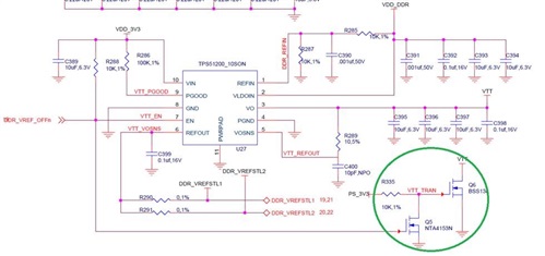
Customer has a question about using TPS51200 to provide power supply to DDR3’ VTT. They want to know below two MOSFET’s purpose and if they take away these two MOSFET, if these is any influence for the total system? Thanks a lot for your support!

8640.TI_AM572XEVM_REV_A3a.pdf


Best regards,

Sulyn Zhang

  • Hi,

    The purpose of this circuit is to discharge the Vtt power rail quickly when the DDR is placed in self-refresh. I wouldn't recommend removing it.
  • Hi Biser,
    Thanks a lot for your reply! As I'm just touch DDR relevant application, thus I'm still not very clear to understand your reply. But I have to explain clearly to my customer, so would you possible give me some more detailed information about how these two MOSFET works during DDR self-refresh?
    My understanding is that when the 3.3V supply was power down(but why?) and the PS_3V3 still alive, then the Q5 was disabled and Q6 was enabled, thus VTT was pulled down. I can't explain anymore based on the schematic, not sure if my understanding is correct? If not, can you help clarify? Thanks.

    Best regards,
    Sulyn Zhang
  • OK, I will try to explain. U27 is the regulator for Vtt and VREF voltages required by DDR3. When the system goes to low-power mode (for AM57x this is Suspend to RAM), the memory is put in self-refresh. Vtt and VREF voltages are switched off (U27 is turned off by the signal DDR_VREF_OFFn, active low). The same signal turns off Q5, which turns on Q6. Q6 shorts the Vtt rail to GND, draining the capacitors on this rail. When DDR_VREF_OFFn goes high, U27 and Q5 are switched on, Q6 is switched off and Vtt and VREF voltages ramp-up.
  • Biser,

    Many thanks for the explaination, it very clear!

    Last question, If Customer don't need to work in low power mode, can they remove the two MOSFET away and just pull Pin 7(Enable pin of TPS51200) to 3.3V supply(Customer only have one 3.3V supply)?  If the two MOSFET can't take away, do we have reference design for the PS_3V3 supply(Customer only have one 3.3V, if PS_3V3 supply is needed, they have to design it).

    Best regards,

    Sulyn Zhang

  • Yes, they can remove the MOSFETs, but I would still recommend to leave the Enable connection as it is. You don't want VREF and Vtt to ramp up earlier than necessary.

    I don't understand your question about PS_3V3. This is generated by U3 on the EVM, and this is the PMIC main supply rail.