This thread has been locked.

If you have a related question, please click the "Ask a related question" button in the top right corner. The newly created question will be automatically linked to this question.

C6672 - Main PLL issue / power failure on target CPU

Other Parts Discussed in Thread: CDCE62005, UCD9222, UCD7242

We have developed a custom PCB based on the C6672 DSP. Most of the boards produced work fine, however, there are still a few that seem to have a Main PLL related issue. The issue already occurs during the startup phase, when the Main PLL initialisation is done using the TI platform library for the C6678.

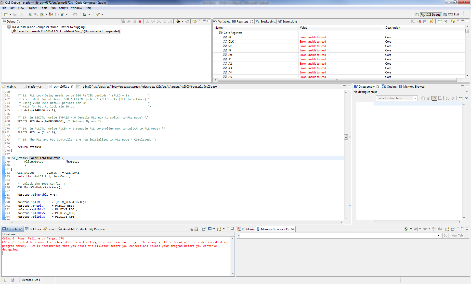
When debugging in CCS5, the debugger reports a 'Power Failure on Target CPU'. For 2 of our boards I can pinpoint the problem to the function CorePllcHwSetup(). More specifically, to step 14 in that function, as described in section 3.1.1 of SPRUGV2G. In that step the PLL controller mux is enabled to switch to PLL mode through the C statement 'PLLCTL_REG |= (1 << 0);'. As soon as I step over that statement, the DSP crashes and the debugger reports as below:

If I enable the option 'Allow power transitions while running if supported (low power running)' in the debug configuration, the target will continue for a bit longer, but then crash as well. Usually, when I try to pause the target then, the debugger will report 'Trouble Halting Target CPU: Connect to PRSC failed'.

What we would like to know is:

1) what could be the root cause of this problem?

2) if no specific root cause can be named, what would be the best way to tackle this problem? Which signals to verify / what register values to check etc?

Any help regarding this problem would be greatly appreciated!

Best regards,

Oane Kingma

  • It seems you are trying to configure the PLL using C source file but how about the gel file ?
    Have you tried to use the gel file ?
    Are you facing any issue while loading the gel file on DSP ?
  • The GEL file loads successfully. However, when running 'Global_Default_Setup', similar results as with the C file as far as I can see:

    Best regards,
    Oane

  • Seems problem with HW, so our HW expert assist you soon.
  • This is a very unusual issue.  PLL configuration and operation problems are rare.

    Since the problem appears in the GEL, I agree that this looks like a hardware issue.  So you have access to a C6678 EVM?  Comparative testing of the code on the EVM may also provide some insight.

    Each of the PLLs has its own filtered power supply.  You need to verify that the power supply implementation matches the requirement stated in the Hardware Design Guide.

    Is this a new board design?  How many have been produced?  How many fail?  Can this be an assembly issue?

    Tom

  • Hi Tom,

    Yes, this is a new design. 40 PCBs have been produced, out of which 36 do not exhibit any problems. Two of the PCBs show the problem as described above. An assembly issue does not seem likely as we've actually had one of these boards X-rayed and everything appears in order.

    The boards have been designed using the Hardware Design Guide, but we'll triple check it also just to be certain.

    Do you have any guidelines on how to continue?

    Best regards,
    Oane

  • Hi Oane,
    Have you checked the stability of the core voltage at the time that the PLL is enabled? Once the PLL is programmed, the power consumption of the part will jump to a higher level and that transition can occur rapidly. If the power supply circuit or the power delivery network on your PCB cannot keep the core voltage within spec during the transition, the SoC may not operate correctly.
    Have you checked the frequency on the SYSCLKOUT pin? We have also seen cases where the PLL was incorrectly programmed, resulting in a higher clock frequency then that part was designed to handle. This could also cause the connection to fail.
    Regards,
    Bill
  • Hi Bill,

    SYSCLKOUT pin shows 16.6 MHz up until the step 14 as described in my original post. As soon as I step over that statement, SYSCLKOUT drops to 0.

    • All our boards use the same TI platform library routine to initialise the PLL, so the incorrect programming scenario seems unlikely.
    • The frequency of the CORECLKx signal also seems ok, as SYSCLKOUT shows 16.6 MHz, which is 100 MHz/6...
    • We use the same clock generator (TI CDCE62005) with the same settings across all 40 produced PCB's.

    As for the core voltage: I'll ask my colleague take a better look at it, but measuring on a test point right after the core voltage power supply does not show any stability issues with the core voltage as far as I can see (Hameg 350 MHz scope set to 20ns/div, 500 mV/div, trigger set to slope down at 970 mV -> no trigger observed).

    Thank you all for your thoughts up to this point, your ideas are greatly appreciated. If you can think of any other, don't hesitate...


    Best regards,

    Oane

  • What do you see on the SYSCLKOUT pin on a board that does not fail?
  • I'll double check it tomorrow, but I'm fairly certain it was 166.6 MHz for the good cards after they've passed step 14 of the PLL initialisation (as it should be...).

    Best regards, Oane

  • Double check completed: on a good card, the SYSCLKOUT shows 16.6 MHz up until step 14. After step 14 (at the end of  CorePllcHwSetup() ) it's 166.6 MHz, as one would expect...

  • I've tried to modify the PLL configuration values a bit to see if the DSP would initialize at lower clock speeds.

    Normal settings:

    1. Clock input frequency: 100 MHz
    2. PLL prediv value = 1
    3. PLL multiplier value = 20
    4. PLL postdiv value = 2

    The final PLL output value should be: (100/1 * (20/2)) = 1.0 GHz. Verified by measuring SYSCLKOUT on a working PCB, which correctly measures 1GHz / 6 = 166.6 MHz.

    Now I've modified the PLL configuration parameters as such:

    1. Clock input frequency: 100 MHz
    2. PLL prediv value = 1
    3. PLL multiplier value = 2
    4. PLL postdiv value = 2

    This should yield a PLL output value of (100/1 * (2/2)) = 100 MHz

    The result: after step 14, the DSP still crashes, even though the clock frequency for the DSP has effectively not changed. Is it safe to say that this rules out a power consumption issue for the core voltage? Or does switching to the PLL also result in more components being enabled?

  • Oane,

    That last test is not truly valid even though the conclusion drawn may be.  Even though the DSP can start booting in BYPASS with the SYSCLK1 running at 100MHz, the device cannot operate all interfaces at this speed.  The lowest rated speed for SYSCLK1 when using peripherals is 800MHz.

    The results still appear to point to a board issue since you state that the board fails during PLL programming even when you use the EVM GEL file.  This PLL programming sequence is known to be robust.  I recommend that you explore possible issues that may result in core supplies (CVDD and CVDD1) or PLL supplies (AVDDA1/2/3) experience voltage droop.  Similarly, you should review the VSS routing for evidence of current starvation.

    These devices require a Smart Reflex power solution.  What are you using to generate CVDD?  How are you controlling the AVS voltage?  What is the AVS voltage at start-up?

    You may want to consider removing the DSP and installing a new one on a failing board to fully rule out an assembly issue.  X-RAYs of assembled boards do not capture all solder issues such as cold joints.

    Tom

  • Hi Tom,

    thanks for your insight! We will do some additional testing / measuring concerning CVDD/CVDD1 and AVDDA1/2/3 to rule out any voltage drops / current starvation.

    In general, the design is largely based on the C6678 EVM kit, so we're using the same Smart Reflex power solutions (UCD9222/UCD7242). Routing should also have closely followed the EVM.

    One of the two failing boards with this issue already had it's DSP removed and reinstalled with the same end result (hence why we had it X-rayed...).

    Hopefully we can find something that explains this issue next week!
  • Oane,

    Since you have the UCD9222 digital power controller implemented on your board, you can also review its fault logs to see if there are any transient events that it is detecting.

    Are you using the UCD configuration files directly from the EVM website or did you revised them to match your design?  It is important that the digital control loop is customized for the exact power stage components implemented on your board.  It is also very important to keep the sensitive analog circuitry separate from the AC ripple currents of the power stage.  This requires special care in the ground implementation around both UCD devices.

    Tom

  • Hi Tom,

    After some measurements, it does not seem that a voltage drop for CVDDx or AVDDAx is the problem. The voltages are all stable when debugstepping over step 14. As for the AVS voltage, it's 1.1V at startup, and then gets adjusted by the Smart Reflex system.


    So far I haven't been able to check the fault logs of the UCD9222 power controller (haven't fully figured out how to show the historic fault values...). However, the configuration file (.xml) we use is similar to the one from the EVM website, apart from some of the values that it's reading... The schematics are also heavily based on the EVM, so I wouldn't expect to find a lot of differences there...


    Best regards,

    Oane

  • Oane,

    Can you disable the AVS control in the UCD configuration so that the voltage remains at 1.1V?  Does this resolve the issue?  Other options may be to supply the voltages one at a time with an external bench supply and see if you can isolate one as a specific contributor.

    The documentation for the Fusion Digital Power Designer should step you though the steps for monitoring voltages and viewing logged faults.

    Tom

  • Hi Tom,

    after some modifications to our power sequencing software, I can now manually enable CVDD and CVDD1 during the power sequence. This allows me to check the actual voltages / currents during powerup until step 14 and after...

    Observations so far:
    * on both defective cards the current consumption on rail #1 is significantly higher (500mA or more) in comparison with good cards up until step 14 and after (when the card crashes). On good cards the current consumption only increases to this level when the main clock is switched to the 1GHz PLL clock.
    * on both defective cards the UCD9222 observes no FAULT conditions!
    * card #1: rail #1 stabilizes at 1.08V, rail #2 stabilizes at 1.0V
    * card #2: rail #1 stabilizes at 1.035V, rail #2 stabilizes at 1.0V

    I haven't been able to find how to disable AVS in the software so far, so I can't comment yet whether that helps.

    My question: is it likely that the increased current drawn from rail #1 contributes to the problem? After all, the UCD9222 does not observe any FAULT conditions...

    Best regards,
    Oane
  • Oane,

    Leakage current variations chip to chip can explain this difference.  What are the absolute measurements?

    I look forward to seeing the results with AVS disabled.  The is a single check-box in the AVS tab in the Fusion Digital Designer tool to disable this.

    Tom

  • Hi Tom,

    it took a lot of searching, but I used 'Ignore VID input pins and commands' for this particular rail to disable AVS.

    Unfortunately, still no luck. Still seeing the same 'Power failure on target CPU' message when single stepping over step 14 of the Main PLL initialisation routine.

    Attached are an Excel file with the logged data from the UCD9222 and the Fusion Digital Power designer XML file used to configure the UCD9222 on the PCB at fault. The logged data was gathered while I manually enabled both rails (rail #1 first, then rail #2) and then loaded the debug program which performs the Main PLL initialisation through the platform library. As can be seen, no drop in voltage on the rails is observed, nor is any additional current drawn. Very strange.

    Hopefully you have some more ideas on how to tackle this problem!

    Best regards,

    Oane

    20161111_026_UCD9222_logging.xlsxUCD9222 @ PMBus Address 78d - ACM 026 AVS off.xml

  • Oane,

    The logging is at a period of 500ms.  It will not capture short term variations.  That was why I was asking about logged warnings.

    So far you have not found any power supply anomaly.  You have disabled the AVS control so that you are forcing the supply and device to operate at the highest rated voltage.  Even then, you are seeing issues during PLL reconfiguration.

    This still points to come type of physical connectivity or filtering issue that results in improper voltage / insufficient current to the die that causes the PLL to misbehave.  I recommend that you recheck your schematic symbol and all power and ground connections in your schematic and PCB layout.  Perhaps you have some power or ground balls that are isolated or have constricted supply.  Also, make sure that all of the reserved pins are properly biased.

    Tom

  • Was the solution ever found?

  • Raz,

    If you have a similar problem, please provide details for your issue.  Also, please perform the same debug steps listed in this thread.  I am assuming that the original thread ended when the original author found the problem based on the debugging questions asked.

    Tom

  • @Raz Aloni: unfortunately, no, we have not been able to locate or solve this problem. For us it is a bit worrisome, in case we're ever going to produce a new batch of boards.

    Since you're asking here, I assume you've had similar experiences. Should you come across a solution, we would greatly appreciate it if you could share it here. We will do the same.