This thread has been locked.
If you have a related question, please click the "Ask a related question" button in the top right corner. The newly created question will be automatically linked to this question.
Hi,
I would like you to confirm about below.
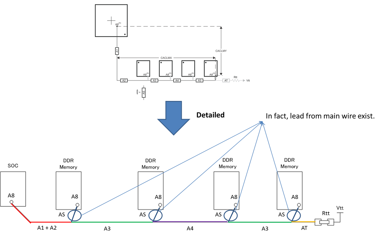
* According to datasheet, there is following figure in DDR section.
There are some parameters(A1, A2..) in this figure, but there is no definition for each parameters.
(For example, A1 means "Device Breakout", A2 means "main PCB" etc..)
Could you please give me definition for each parameters ?
Best Regards,
Machida
Hi Pavel-san and Yordan-san,
Thank you for your reply.
Yes, I confirmed Table 9-28, but there is uncleared point in this table. So I asked there is exactly definition for each parameters(A1, A2.. etc) in document.
According to E2E information which Pavel-san suggested, I understood as shown below for each paramaters.
Could you please confirm just in case ?
A1+A2 : Device breakout + trace to first DDR memory
A3 : the stump from the trace to next DDR memory
A4 : the stump from the trace to next DDR memory
AS : the stump from the trace to the chip
AT : the stump from the trace to DDR termination resistor
Best Regards,
Machida