This thread has been locked.

If you have a related question, please click the "Ask a related question" button in the top right corner. The newly created question will be automatically linked to this question.

RTOS/TMS320C6678: SRIO DIO operation

Part Number: TMS320C6678

Tool/software: TI-RTOS

Hi
I have a customized board that contained FPGA and DSP. I want to send data from FPGA to DSP by SRIO.
I want to FPGA write data in DSP memory. After I studied " sprugw1b.pdf " I decided to use DIO and I run
" C:\ti\pdk_C6678_1_1_2_6\packages\ti\drv\exampleProjects\SRIO_LoopbackDioIsrexampleproject " examples.

According to " sprugw1b.pdf " page 63 if packet type is NREAD, NWRITE  ..., DSP is in DIO operation mode in
other words when FPGA send packets including SWRITE,NREAD, NWRITE, DSP received DIO packets.

Q 1:
Which field of header in FPGA is responsible  for DSP memory map address?

I studied " pg007.pdf " in page 168 describe the packet format as below.
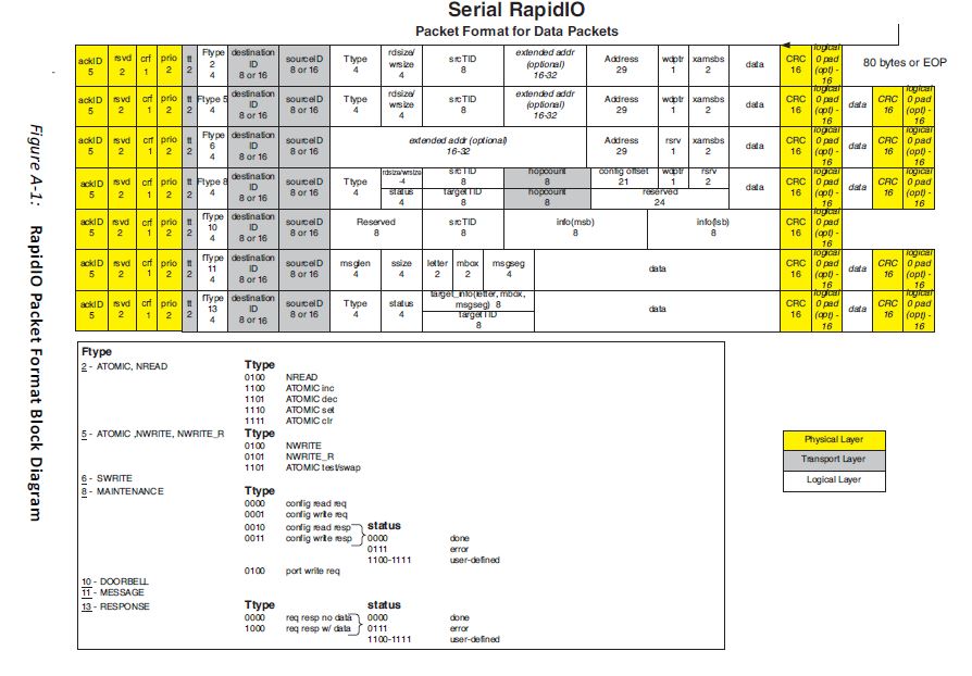
Q 2:
Which field of frame determine the DSP memory address in the figure 2-11 in " sprugw1b.pdf " as below?

Q 3:
Why " WrPtr " is one byte?

Best Regards

  • Hi Dariush,

    I've forwarded this to the SRIO experts. Their feedback should be posted here.

    BR
    Tsvetolin Shulev
  • Hi,

    Q1/2:

    address + ext_addr + xamsbs form 63 bits address. Since SRIO requires double-word alignment and the SRIO addressing is 66 bits wide (or 34 or 50 depending on the size of the ext_addr filed), the address in the SRIO packet is a double word address. The missing 3 lsb and the unaligned bytes are coded in the wrsize+wrprt.

    Since the dsp addresses are 32 bits wide:
    address=dsp_address >> 3
    ext_addr=0
    xamsbs=0

    Q3: WrPtr is 1 bit wide (not 1 byte) and together with rdsize/wrsizee encode both the size and the "bytes lane" depending on the alignment
    (wrsize,wrptr)=encode(bytes_count, dsp_address & 0x7)
    For the encode() algorithm, look at SRIO specification.

    If your playload destination address in not double-word aligned and is longer then 7 bytes, the transfer must be broken in more packets:
    1. Leading unaligned bytes, len=dsp_address & 0x7, to align next transfers
    2. one or more 256 bytes fragments, double-word aligned
    3. Trailing unaligned bytes (up to 7 bytes)
  • Hi

    Thank you so much, Alberto.

    Please, guide me I understand you correctly.

    Ftype 5 (NWRITE): 

    I should accomplish this steps for writing in DSP:

    1) I should shift DSP address 3 bits right and write the address in the address field of the header.

    2) I should set "ext_addr" and "xamsbs" zero.

    3) I should set WrPtr and WrSize according to 3 remain lsb bits and encoding algorythms.

    Q 1:

    I studied the "sprugw1b.pdf " and there wasn't anything about encoding algorythm!!!

    Please introduce me a reference that explained encode algorithm or how can I set "WrPtr" and "WrSize" fields?

    Ftype 6(SWRITE):

    There isn't "WrPtr" and "WrSize" in the header fields. 

    Q 2:

    Is the writing steps same as Ftype5?

    If the answer is yes what should I do about "WrPtr" and "WrSize" fields?

    If the answer is NO, guide me please.

    Regards

  • Hi

    Please, answer me. I'm waiting for you.

    Regards

  • Why nobody answer me?

  • Hi,

    I've escalated this internally.

    Best Regards,
    Yordan
  • Dariush,

    The details of forming RapidIO packet header is not described in Keystone Serial RapdioIO user guide sprugw1b as the SRIO Load/Store unit (LSU) in Keystone provides the mechanism to abstract and auto fill all the header fields of the RapidIO packet. There are 8 LSU in total, and each LSU has its own set of 7 registers. LSU_Reg0-4 is used to store “Control” information, LSU_reg5-6 for “Command” and Status information. You may check with your FPGA vendor to see if there is similar mechanism/module for structuring RapidIO packet header.

    RapidIO in Keystone is RapidIO Interconnect Specification REV2.2 compliant. You may also look into the document - RapidIO™ Interconnect Specification, Part 1: Input/Output Logical, Chapter 4 Packet Format Descriptions, www.rapidio.org/.../, for DirectIO packet header field description.

    wdptr: Word pointer, used in conjunction with the data size (rdsize and wrsize) fields—see Table 4-3, Table 4-4 and Section 3.5.
    rdsize: Data size for read transactions, used in conjunction with the word pointer (wdptr) bit—see Table 4-3 and Section 3.5.
    wrsize: Write data size for sub-double-word transactions, used in conjunction with the word pointer (wdptr) bit—see Table 4-4 and Section 3.5.

    In general, the steps you listed for Ftype 5 is correct. For "WrPtr" and "WrSize" fields setting, refer to above description.
    For Ftype 6, there is no size or transaction ID fields, so basically you just need step 1 and 2, please refer to 4.1.8 Type 6 Packet Format (Streaming-Write Class) in RapidIO spec.

    Regards,
    Garrett
  • Hi

    Thank you so much, I got my answer.

    I have some new answer, If you want I start new thread.

    I set " C:\ti\pdk_C6678_1_1_2_6\packages\ti\drv\exampleProjects\SRIO_TputBenchmarkingTestProject " as my base project for communicating to FPGA by SRIO.

    I accomplished this steps:

    1) set port to the normal mode

    2) set the board to board macro TRUE.

    3) load the program on Core0, but some problems happen.

    Port didn't initialized, I checked the SPn_ERR_STAT and it,s value was " 0x00000001 ".

    Q 1:

    What should I do for solving this problem? I checked more STATUS registers but I couldn't solve the problem. Please guide.

    I want the FPGA be master in the communication between DSP and FPGA, I found SP_GEN_CTL(0xB13C) that it's value was " 0x00000000 ".

    Q 2:

    Is it necessary to change the SP_GEN_CTL values?

    Q 3:

    When link between DSP and FPGA produce error(uninitialized), How can I debug it and solve the problem?

    Regards

  • Please, answer me!!! 

  • Hi 

    Why nobody answer!!!!!

  • dariush,

    Were you able to successfully run the SRIO_TputBenchmarkingTestProject cross boards? As noted in Readme.txt,


    To test board to board at same port width and baud rate shown above, the following
    changes to the global variables will be needed: (Boards will need to be connected
    through break-out cards are using a chassis with an sRIO switch.
     On the Consumer EVM (RX side, load .out file on core 0):
       1) testControl.srio_isLoopbackMode = FALSE;
       2) Start consumer application before starting the producer application.
     On the Producer EVM (TX side, load .out file on core 1):
       1) testControl.srio_isLoopbackMode = FALSE;
       2) testControl.srio_initCorenum = 1;
       3) Start the producer after the consumer


    How does your DSP connect to FPGA? Are these devices on a custom board of yours? Have you verified the port physical connection, lane width and baud rate setting in both devices? If you are able to run the DSP board to board benchmarking test, have you contacted your FPGA vendor for the port initialization issue?

    This e2e thread may help: e2e.ti.com/.../224579

    The MASTER_ENABLE bit should have been set in SP_GEN_CTL(0xB13C). The latest PDK 2.0.6 for C6678 is available here: software-dl.ti.com/.../index_FDS.html

        /* Set the Port General CSR: Only executing as Master Enable */
        CSL_SRIO_SetPortGeneralCSR (hSrio, 0, 1, 0);

    Regards,
    Garrett

  • Hi
    Thank you so much, Please help me.
    At first I explained my former works:
    1) I studied " sprugw1b.pdf ".
    2) I run all TI SRIO examples in " C:\ti\pdk_C6678_1_1_2_6\packages\ti\drv\exampleProjects " in loop back mode successfully.
    3) I'm working on a customized board, FPGA is connected to DSP by SRIO. I did a test between FPGA and DSP
    by SRIO successfully as below:
    3_1) My base project was " SRIO_TputBenchmarkingTestProject ".
    3_1) testControl.srio_isLoopbackMode = FALSE;
    3_2) testControl. srio_laneSpeedGbps = srio_lane_rate_3p125Gbps;
    3_3) FPGA was in Loopback.
    Core0 and Core1 communication together via FPGA and example run successfully.

    Now I want FPGA work as master and write the data to DSP memory.
    I did some changes in the " SRIO_TputBenchmarkingTestProject " project.
    First:
    1)I commented NREAD and type11 test functions in the consumerTests(); and producerTests(); functions.
    2) For NWRITE I simplified the code and core0 could write data in the L2SRAM of core1 successfully.
    I tested in loopback mode.

    Second:
    I modify project of in the first step for communicating to FPGA.
    1) testControl.srio_isLoopbackMode = FALSE;
    2) testControl. srio_laneSpeedGbps = srio_lane_rate_3p125Gbps;
    3) testControl.srio_isBoardToBoard = TRUE;
    4) I loaded the project on Core0.
    When I run the DSP project, Port didn't initialized, I checked the SPn_ERR_STAT and it,s value was " 0x00000001 ".
    Q 1:
    Is it necessary to do more changes in the " SRIO_TputBenchmarkingTestProject " project.
    Please guide me.

    Best Regards
  • dariush,

    For the 'FPGA loopback', do you mean your are simply routing the DSP's SRIO Tx to Rx pairs via FPGA?

    While the 'FPGA loopback' works but 'Port didn't initialized' when communicating to FPGA, which seems indicate the FPGA is not initialized properly for port physical connection, lane width or baud rate, and you should not need more changes in the " SRIO_TputBenchmarkingTestProject " project to just get port_OK. I suggest you to contact your FPGA vendor to move forward.

    Regards,
    Garrett