This thread has been locked.

If you have a related question, please click the "Ask a related question" button in the top right corner. The newly created question will be automatically linked to this question.

AM3352: DDR3 software leveling issue

Part Number: AM3352

Hello TI Team,


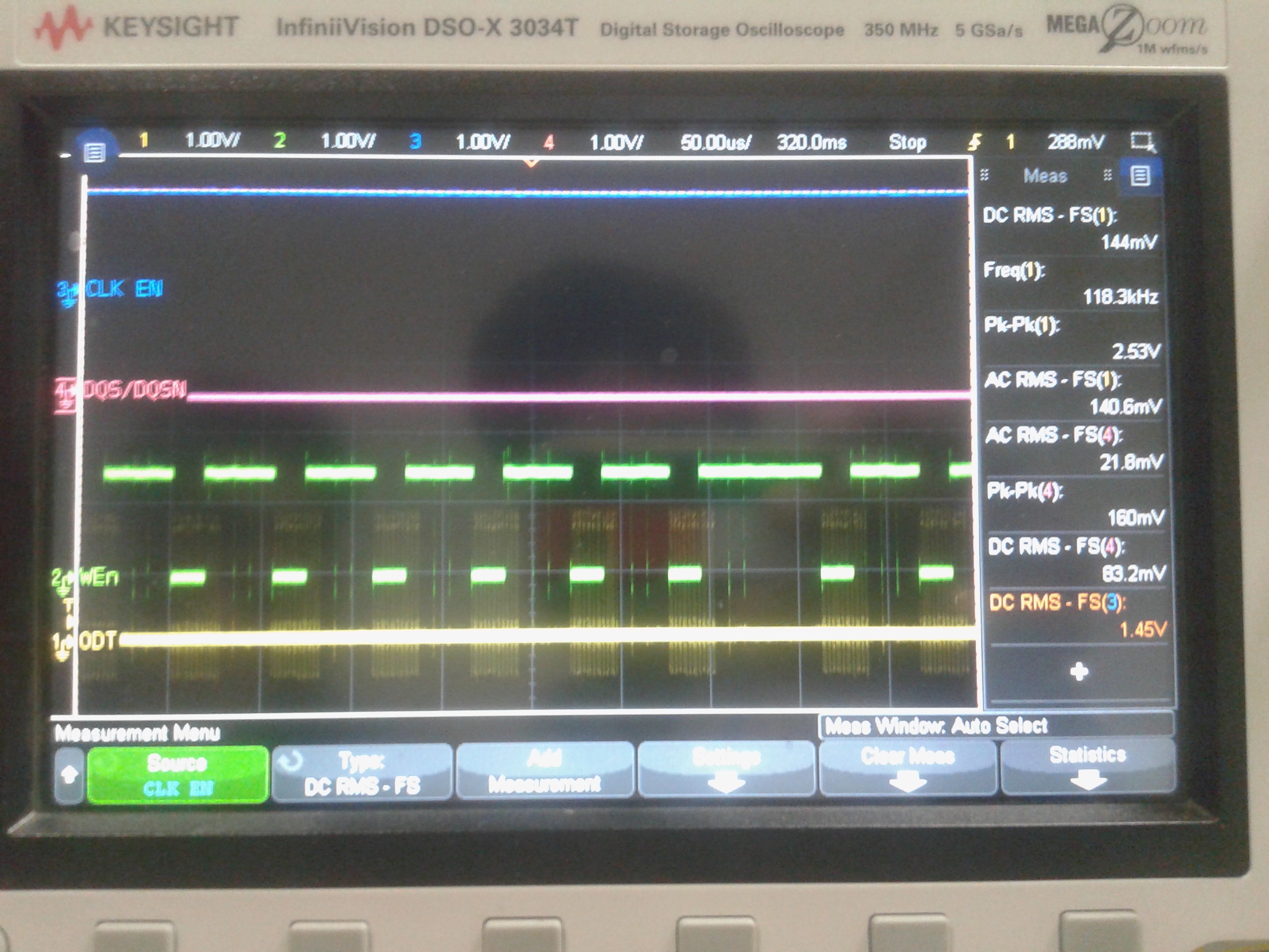
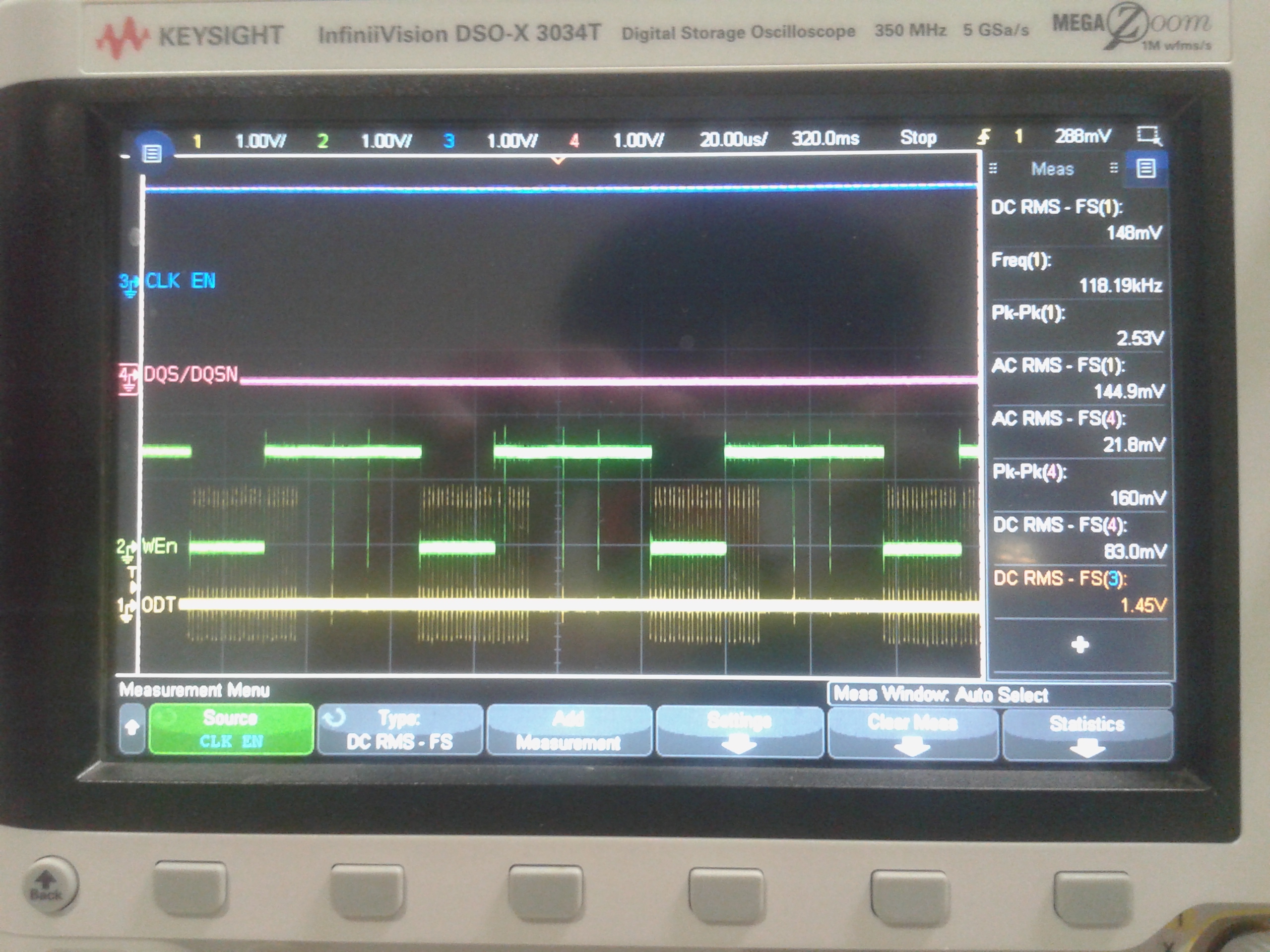
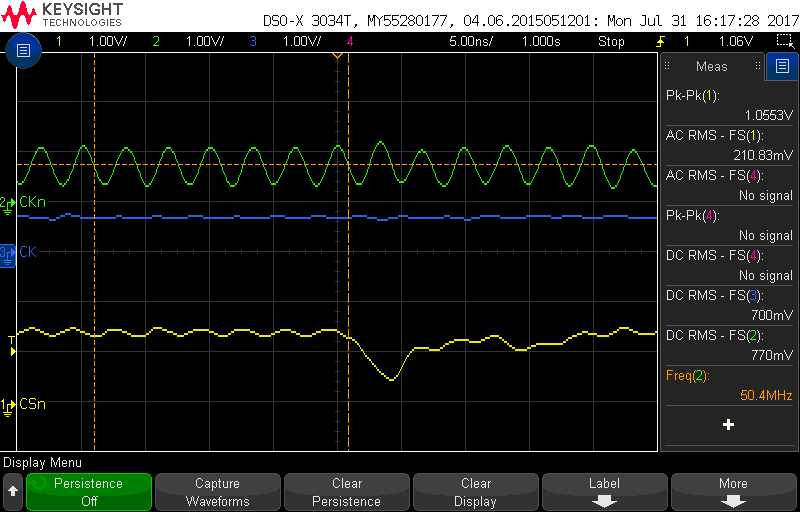
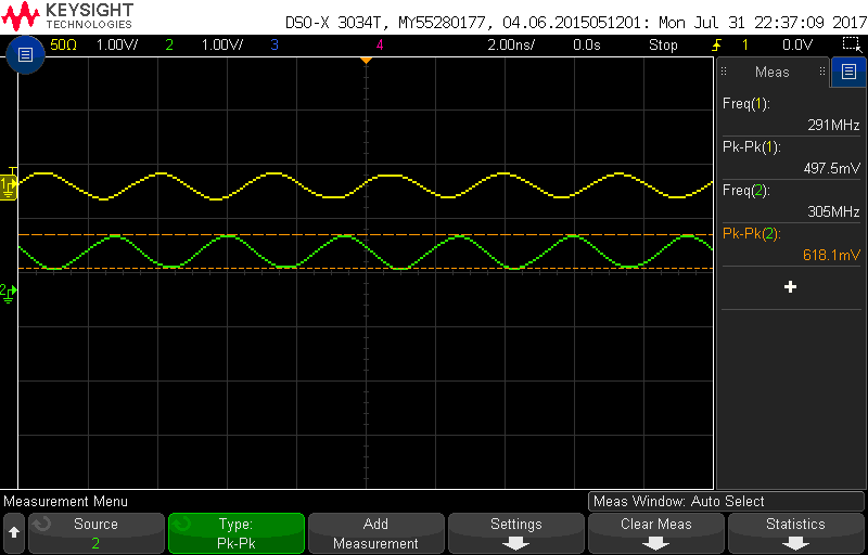
We are using AM3352 with ISSI DDR3 "IS43TR16256A-125KBLI" in one of our project. We have used XDS200 USB Emulator in one of our project and able to connect the JTAG.

After connecting the JTAG and checking the Test connection we are getting the logs as follows:


[Start: Texas Instruments XDS2xx USB Debug Probe_0]

Execute the command:

%ccs_base%/common/uscif/dbgjtag -f %boarddatafile% -rv -o -S integrity

[Result]


-----[Print the board config pathname(s)]------------------------------------

D:\Users\kumar_ne\AppData\Local\TEXASI~1\
    CCS\ti\0\0\BrdDat\testBoard.dat

-----[Print the reset-command software log-file]-----------------------------

This utility has selected a 560/2xx-class product.
This utility will load the program 'xds2xxu.out'.
The library build date was 'May 23 2017'.
The library build time was '19:03:48'.
The library package version is '6.0.628.3'.
The library component version is '35.35.0.0'.
The controller does not use a programmable FPGA.
The controller has a version number of '13' (0x0000000d).
The controller has an insertion length of '0' (0x00000000).
This utility will attempt to reset the controller.
This utility has successfully reset the controller.

-----[Print the reset-command hardware log-file]-----------------------------

This emulator does not create a reset log-file.

-----[Perform the Integrity scan-test on the JTAG IR]------------------------

This test will use blocks of 64 32-bit words.
This test will be applied just once.

Do a test using 0xFFFFFFFF.
Scan tests: 1, skipped: 0, failed: 0
Do a test using 0x00000000.
Scan tests: 2, skipped: 0, failed: 0
Do a test using 0xFE03E0E2.
Scan tests: 3, skipped: 0, failed: 0
Do a test using 0x01FC1F1D.
Scan tests: 4, skipped: 0, failed: 0
Do a test using 0x5533CCAA.
Scan tests: 5, skipped: 0, failed: 0
Do a test using 0xAACC3355.
Scan tests: 6, skipped: 0, failed: 0
All of the values were scanned correctly.

The JTAG IR Integrity scan-test has succeeded.

-----[Perform the Integrity scan-test on the JTAG DR]------------------------

This test will use blocks of 64 32-bit words.
This test will be applied just once.

Do a test using 0xFFFFFFFF.
Scan tests: 1, skipped: 0, failed: 0
Do a test using 0x00000000.
Scan tests: 2, skipped: 0, failed: 0
Do a test using 0xFE03E0E2.
Scan tests: 3, skipped: 0, failed: 0
Do a test using 0x01FC1F1D.
Scan tests: 4, skipped: 0, failed: 0
Do a test using 0x5533CCAA.
Scan tests: 5, skipped: 0, failed: 0
Do a test using 0xAACC3355.
Scan tests: 6, skipped: 0, failed: 0
All of the values were scanned correctly.

The JTAG DR Integrity scan-test has succeeded.

[End: Texas Instruments XDS2xx USB Debug Probe_0]


Going further with the reference of TI wiki processors.wiki.ti.com/.../Sitara_Linux_Training:_Tuning_the_DDR3_Timings_on_BeagleBoneBlack      


After uploading the customized gel file and downloaded . out file, we are unable to get the optimized DDR register optimized values.


Values are as follows:


[CortxA8]
Enter the PHY_INVERT_CLKOUT value (0 or 1) from the spreadsheet
0

Enter the Seed RD_DQS_SLAVE_RATIO Value in Hex to search the RD DQS Ratio Window
40

Enter the Seed FIFO_WE_SLAVE_RATIO Value in Hex to search the RD DQS Gate Window
8C

Enter the Seed WR_DQS_SLAVE_RATIO Write DQS Ratio Value in Hex to search the Write DQS Ratio Window
0

***************************************************************
 The Slave Ratio Search Program Values are...
***************************************************************
PARAMETER                       MAX  |  MIN  | OPTIMUM |  RANGE
***************************************************************
DATA_PHY_RD_DQS_SLAVE_RATIO    0x000 | 0x000 |  0x000  | 0x000
DATA_PHY_FIFO_WE_SLAVE_RATIO   0x000 | 0x000 |  0x000  | 0x000
DATA_PHY_WR_DQS_SLAVE_RATIO    0x000 | 0x000 |  0x000  | 0x000
DATA_PHY_WR_DATA_SLAVE_RATIO   0x000 | 0x000 |  0x000  | 0x000
***************************************************************
rd_dqs_range = 0
fifo_we_range = 0
wr_dqs_range = 0
wr_data_range = 0

Optimal values have been found!!

***************************************************************
 The Slave Ratio Search Program Values are...
***************************************************************
PARAMETER                       MAX  |  MIN  | OPTIMUM |  RANGE
***************************************************************
DATA_PHY_RD_DQS_SLAVE_RATIO    0x000 | 0x000 |  0x000  | 0x000
DATA_PHY_FIFO_WE_SLAVE_RATIO   0x000 | 0x000 |  0x000  | 0x000
DATA_PHY_WR_DQS_SLAVE_RATIO    0x000 | 0x000 |  0x000  | 0x000
DATA_PHY_WR_DATA_SLAVE_RATIO   0x000 | 0x000 |  0x000  | 0x000
***************************************************************

===== END OF TEST =====


Please do let us know the probable solution here. Please suggest the resolution to resolve the issue.

8484.RatioSeed_AM335x_boards.xls8802.AM335x_DDR_register_calc_tool.xlsvector-eye_main-board_25_05_2017.pdf

  • Your schematic does not comply to the DDR3 design requirements. No serial resistors are permitted on DDR3 signal lines. Please follow the guidelines in section 7.7.2.3 of the AM335x Datasheet Rev. J.
  • Hi Biser,
    Thanks for prompt reply.

    I have unplaced all the serial resistors from Command/Address and Data lines and shorted the resister pads. But I am getting the same response.
    Still the optimized values are 0. Please suggest.

    Regards,
    Daljeet
  • You are using a point-to-point connection for your DDR, with no termination. Section 7.7.2.3.3.9 of the AM335x Datasheet Rev. J states:

    "Signal terminations are required for the CK and ADDR_CTRL net class signals. On-device terminations (ODTs) are required on the DQS[x] and DQ[x] net class signals. Detailed termination specifications are covered in the routing rules in the following sections.

    Figure 7-48 provides an example DDR3 schematic with a single 16-bit DDR3 memory device that does not have VTT termination on the address and control signals. A typical DDR3 point-to-point topology may provide acceptable signal integrity without VTT termination. System performance should be verified by performing signal integrity analysis using specific PCB design details before implementing this topology."
  • Hi Biser,

    This is Nikhil. I am working with Daljeet on the same issue. We have started the signal integrity analysis for our design, Meanwhile I would like to share the PHY and EMIF calculation sheets as well as the DDR3 datasheet that we are using to update the GEL file. Max. Processor frequency is 300 MHz. We also tried to change multiple values in GEL file but nothing worked. Attached are the 3 files. We are using the GEL file provided on http://processors.wiki.ti.com/index.php/File:BeagleBlack_400Mhz_4GbDDR.gel.tar.gz and updating the EMIF values we get using the excel sheet tool.

    Regards0310.AM335x_DDR_register_calc_tool.xlsDDR3 ISSI.PDF4643.RatioSeed_AM335x_boards.xls

  • The only error I found in your timings is that tRAS should be 35ns, not 36. Can you try the leveling with 303MHz DDR clock?
  •   Hi Biser,

    Today we have tried to probe the signals , we have probe the DQS/DQSn (Strobe signal), CKE (Clock Enable), WE (Write Enable) and ODT (On-die termination) signals. While executing write command, WE assert low, CKE enable is high and ODT asserts high, but there is no DQS/DQSn signals from AM3352.

    Please check the attached waveform for your reference and suggest.

    Regards,

    Daljeet

  • This is not normal. What is running on the AM335x when you are taking these screenshots? Are you sure the EMIF is properly initialized? Do you see this on a single board or across multiple boards?
  • ISSI_DDR3_43-46TR16256A-85120AL.pdfAM335x_SK_1.2.gel2100.AM335x_DDR_register_calc_tool.xls6813.RatioSeed_AM335x_boards.xlsThese Waveforms has been captured while generating the optimized PHY register values.

    We have tried to read back the EMIF and PHY register values in GEL file and the logs are as follows:

    CortxA8: Output: ****  AM335x BeagleBlack Initialization is in progress ..........

    CortxA8: Output: ****  AM335x ALL PLL Config for OPP == OPP100 is in progress .........

    CortxA8: Output: Input Clock Read from SYSBOOT[15:14]:  24MHz

    CortxA8: Output: ****  Going to Bypass...

    CortxA8: Output: ****  Bypassed, changing values...

    CortxA8: Output: ****  Locking ARM PLL

    CortxA8: Output: ****  Core Bypassed

    CortxA8: Output: ****  Now locking Core...

    CortxA8: Output: ****  Core locked

    CortxA8: Output: ****  DDR DPLL Bypassed

    CortxA8: Output: ****  DDR DPLL Locked

    CortxA8: Output: ****  PER DPLL Bypassed

    CortxA8: Output: ****  PER DPLL Locked

    CortxA8: Output: ****  DISP PLL Config is in progress ..........

    CortxA8: Output: ****  DISP PLL Config is DONE ..........

    CortxA8: Output: ****  AM335x ALL ADPLL Config for OPP == OPP100 is Done .........

    CortxA8: Output: ****  AM335x DDR3 EMIF and PHY configuration is in progress.........

    CortxA8: Output: EMIF PRCM is in progress .......

    CortxA8: Output: EMIF PRCM Done

    CortxA8: Output: DDR PHY Configuration in progress

    CortxA8: Output: Waiting for VTP Ready .......

    CortxA8: Output: VTP is Ready!

    CortxA8: Output: DDR PHY CMD0 Register configuration is in progress .......

    CortxA8: Output: CMD0_REG_PHY_CTRL_SLAVE_RATIO_0 0x0x00000000 Read back .......

    CortxA8: Output: CMD0_REG_PHY_INVERT_CLKOUT_0 0x0x00000000 Read back .......

    CortxA8: Output: DDR PHY CMD1 Register configuration is in progress .......

    CortxA8: Output: CMD0_REG_PHY_CTRL_SLAVE_RATIO_0 0x0x00000000 Read back .......

    CortxA8: Output: CMD0_REG_PHY_INVERT_CLKOUT_0 0x0x00000000 Read back .......

    CortxA8: Output: DDR PHY CMD2 Register configuration is in progress .......

    CortxA8: Output: CMD0_REG_PHY_CTRL_SLAVE_RATIO_0 0x0x00000000 Read back .......

    CortxA8: Output: CMD0_REG_PHY_INVERT_CLKOUT_0 0x0x00000000 Read back .......

    CortxA8: Output: DDR PHY DATA0 Register configuration is in progress .......

    CortxA8: Output: DATA0_REG_PHY_RD_DQS_SLAVE_RATIO_0 0x0x00000000 Read back .......

    CortxA8: Output: DATA0_REG_PHY_WR_DQS_SLAVE_RATIO_0 0x0x00000000 Read back .......

    CortxA8: Output: DATA0_REG_PHY_FIFO_WE_SLAVE_RATIO_0 0x0x00000000 Read back .......

    CortxA8: Output: DATA0_REG_PHY_WR_DATA_SLAVE_RATIO_0 0x0x00000000 Read back .......

    CortxA8: Output: DDR PHY DATA1 Register configuration is in progress .......

    CortxA8: Output: DATA0_REG_PHY_RD_DQS_SLAVE_RATIO_0 0x0x00000000 Read back .......

    CortxA8: Output: DATA0_REG_PHY_WR_DQS_SLAVE_RATIO_0 0x0x00000000 Read back .......

    CortxA8: Output: DATA0_REG_PHY_FIFO_WE_SLAVE_RATIO_0 0x0x00000000 Read back .......

    CortxA8: Output: DATA0_REG_PHY_WR_DATA_SLAVE_RATIO_0 0x0x00000000 Read back .......

    CortxA8: Output: Setting IO control registers.......

    CortxA8: Output: DDR_CKE_CTRL0x0x00000001 Read back .......

    CortxA8: Output: EMIF Timing register configuration is in progress .......

    CortxA8: Output: EMIF_DDR_PHY_CTRL_1_REG 0x0x00000006 Read back .......

    CortxA8: Output: EMIF_DDR_PHY_CTRL_1_SHDW_REG 0x0x00000006 Read back .......

    CortxA8: Output: EMIF_DDR_PHY_CTRL_2_REG 0x0x00000006 Read back .......

    CortxA8: Output: EMIF_SDRAM_TIM_1_REG 0x0x0888A39B Read back .......

    CortxA8: Output: EMIF_SDRAM_TIM_1_SHDW_REG 0x0x0888A39B Read back .......

    CortxA8: Output: EMIF_SDRAM_TIM_2_REG 0x0x26517FDA Read back .......

    CortxA8: Output: EMIF_SDRAM_TIM_2_SHDW_REG 0x0x26517FDA Read back .......

    CortxA8: Output: EMIF_SDRAM_TIM_3_REG 0x0x501F84EF Read back .......

    CortxA8: Output: EMIF_SDRAM_TIM_3_SHDW_REG 0x0x501F84EF Read back .......

    CortxA8: Output: EMIF_SDRAM_REF_CTRL_REG 0x0x0000093B Read back .......

    CortxA8: Output: EMIF_SDRAM_REF_CTRL_SHDW_REG 0x0x0000093B Read back .......

    CortxA8: Output: EMIF_ZQ_CONFIG_REG 0x0x50074BE4 Read back .......

    CortxA8: Output: EMIF_SDRAM_CONFIG_REG 0x0x61A04BB0 Read back .......

    CortxA8: Output: EMIF Timing register configuration is done .......

    CortxA8: Output: PHY is READY!!

    CortxA8: Output: DDR PHY Configuration done

    CortxA8: Output: ****  AM335x BeagleBlack Initialization is Done ******************

    We have calculated the EMIF register values from TI DDR3 Timing configuration tool which is as attached. Please verify the same.

    We have calculated the PHY register values from TI Ratioseed xls file which is as attached. Please verify the same.

    We have checked this in 3 Boards and all boards are behaving same and we are not getting optimized value.

    Question here is that we are not getting clock and DQS signal from AM3352. We need to find out the root cause for the same. Can you suggest what can be the probable reason for the same? Do we need to  configure any register to enable the clock. I am attaching the GEL which have modified for 303MHz and ran today. Please verify the same also.

    While reading the DDR3 datasheet, IS43TR16256A-125KBLI, we came across that Page 14 describes Mode register MR1. Address filed A7 denotes write leveling On/OFF. where we need to set this bit. We are not able to find the same in GEL file. Please check the attached datasheet.

    Regards,

    Daljeet

  • One other thing I notice on the schematics: Try adding a 10k pulldown resistor on DDR_CKE.
  • Hi Biser,
    We have already done this change in our PCB, but no change. Optimized values are still 0.
  •   Hi Biser,

    I have tried to probe the CK and CK#, it seems that we are getting the 300MHz clock at CK# and not in CK. Please suggest.

  • I already pointed out in my initial replies that you have severe design/manufacturing issues. If what you are measuring is really what is shown on those scope screenshots, this board will never work. I have never seen such DDR behavior. On my part I cannot help further with this issue.

    I have notified the factory team to look at this thread. They will post here if they have any suggestions.
  •  Hi Biser,

    Just to check if AM3352 is feeding Clock or not, today I have disconnected the DDR3 by removed serial resistor on CK and CK# pin and I observed the differential clock on the same. Please check the attached waveform.

    It seems to be the DDR Assembly problem or may be DDR chipset gone bad.

    Please do let me know the another thought on the same.

    Regards,

    Daljeet

  • - I think the series resistors might be too big for the I/O drive being set which could be a problem. Try to see if the problem goes away by increasing the I/O drive strength

    - Did you turn the parallel termination on the Data bus on the DRAM and the processor? If so, please disable this since you already have series resistors. Alternately, try a test with removing all the series resistor on the Data bus and enable ODT. For Addr/Ctrl, you can use a smaller value (say 10 ohm) and see if it changes the behavior

    - Can you also check if you have the right CCS configuration esp. if the processor is in supervisor mode. You can refer to the below E2E post for more details

    https://e2e.ti.com/support/arm/sitara_arm/f/791/t/603477

    - Probe the power supplies esp. VDDS_DDR, DDR_VREF at the SoC and VDDQ, VREF_CA/DQ on the memory side and see if they are at proper levels


    Regards, Siva

  •  Hi Siva,

    Today we have successfully get the differential clock of 300 MHz at CK/CK# and validated all the control signals which are (WE#, CS#, RESET#, RAS, CAS, CKE) which are asserted and de-asserted while AM3352 Initialisation.

    But we are not getting the DQS/DQSn strobe clock while Data latch. As a next step we need to find the root cause for the same.

    Please check the attached Differential clock for your reference and let me know your valuable suggestions.

    Regards,

    Daljeet

  • Hi Siva,

    With Biser suggestion, we have removed the series resister on Data, Address/Command and Control signals and ran the tests.

    As of now, the ODT is enabled and we are getting 0.74V at DDR_Vref and 1.48V at VDDS_DDR.

    From GEL file perspective ,

    You shared a GEL file for 303 MHz. In that we saw a difference,

    //*******************************************************************
    //DDR3 PHY parameters
    //*******************************************************************

    #define CMD_PHY_CTRL_SLAVE_RATIO 0x80
    #define CMD_PHY_INVERT_CLKOUT 0x0

    #define DATA_PHY_RD_DQS_SLAVE_RATIO 0x40
    #define DATA_PHY_FIFO_WE_SLAVE_RATIO 0x8C //RD DQS GATE
    #define DATA_PHY_WR_DQS_SLAVE_RATIO 0x00 //0x10
    #define DATA_PHY_WR_DATA_SLAVE_RATIO 0x72 //0x80 //WRITE DATA

    #define DDR_IOCTRL_VALUE (0x18B)

    //******************************************************************
    //EMIF parameters
    //******************************************************************
    #define ALLOPP_DDR3_READ_LATENCY 0x07 //RD_Latency = (CL + 2) - 1
    #define ALLOPP_DDR3_SDRAM_TIMING1 0x0888A39B //0x0AAAD4EB //0x0AAAD4EB
    #define ALLOPP_DDR3_SDRAM_TIMING2 0x26517FDA //0x26377FDA
    #define ALLOPP_DDR3_SDRAM_TIMING3 0x501F84EF //0x501F833F

    #define ALLOPP_DDR3_SDRAM_CONFIG 0x61C05332 //0x61C04AB2//0x61C05332 //termination = 1 (RZQ/4)
    //dynamic ODT = 2 (RZQ/2)
    //SDRAM drive = 0 (RZQ/6)
    //CWL = 0 (CAS write latency = 5)
    //CL = 2 (CAS latency = 5)
    //ROWSIZE = 5 (14 row bits)
    //PAGESIZE = 2 (10 column bits)
    #define ALLOPP_DDR3_REF_CTRL 0x0000093B //0x00000C30 //303 * 7.8us = 0x93B
    #define ALLOPP_DDR3_ZQ_CONFIG 0x50074BE4

    Two questions here ,

    1. #define DATA_PHY_FIFO_WE_SLAVE_RATIO 0x8C . we are getting 0x79 as per the excel sheet. How did you get 0x8C ?

    2. In the ISSI DDR3 Data sheet, we are selecting CL=11, but in GEL file  ALLOPP_DDR3_SDRAM_CONFIG is configured for CL =5, so for, CL=11, we have modified the ALLOPP_DDR3_SDRAM_CONFIG and  AL2870.AM335x_SK_1.2.gelLOPP_DDR3_READ_LATENCY in the attached file above . Please confirm the values are correct . If they are wrong , please let us know the right values/changes to be made.

    Thanks and regards,

    Daljeet.

  • Hi Daljeet,

    please update the DATA_PHY_FIFO_WE_SLAVE_RATIO as per your design. I will let Siva comment on other settings, but as discussed please update the observations on the suggestions given by Siva in previous posts.

    Best Regards,
    Shiv

  • Hi Biser,

    From SW team perspective, we have few queries :

    Based on your feedback, and with the issue that we are facing:

    1.If the DDR3 is not properly initialized , then write leveling could/will run with all zeros, right ?

    2.If write leveling is all zeros , then DQS signal won’t come from processor, right ?

    3.Is there a way to read theDDR3 mode registers from processor before initialization or at any other stage?

    4.In the GEL file provided by TI , We don’t see the MR1 setting, A7 in MR1 set “High” to enter the Write leveling mode. Then how does this bit get SET ?

    5.Also for Software Write leveling, we should set this MR1 A7 set “HIGH” ?

    Your answers for all queries could help us narrow down the issue.

    Thanks and regards,

    Daljeet

  • Hi Biser/Shiva,

    Adding one more query :

    6. In processor, we saw a register named "read-write Leveling control register" Offset =DCh

      Bit 31 : says "1" will trigger the read and write leveling.

        Are we setting this bit and controlling any other parameters in this register?

        I don't see any such related setting in the GEL file.

    Thanks  

    Daljeet.

  • Hi Biser/Shiva,

    Adding to the queries  I have asked earlier, I would like to add one more information :

    This is for 400 MHZ.

    On Probing the DDR Initialization signals (RESET and CKE), we found that CKE is going HIGH in 132uS with respect to RESET HIGH. Expected time is 500uS.

    For this we changed the value of ALLOP_DDR3_REF_CTRL to 0x3100 instead of 0xC30. After making this change, we saw 508uS difference between RESET HIGH and CKE HIGH.

    We assume this as a bug in the GEL file and suspect there could be more settings wrongly set in the GEL file TI shared .

    Could you please let us know , what could be the right  values to be set for 400 MHz (Please don't calculate from the DDR3 timing config tool Spreadsheet  ). ALLOPP_SDRAM_DDR3_TIMING1 ,ALLOPP_SDRAM_DDR3_TIMING2,ALLOPP_SDRAM_DDR3_TIMING3 ,ALLOPP_DDR3_SDRAM_CONFIG,READ_LATENCY and DDR3_ZQ_CONFIG

    Thanks and Regards,

    Daljeet.