This thread has been locked.

If you have a related question, please click the "Ask a related question" button in the top right corner. The newly created question will be automatically linked to this question.

TMS320C6657: Power sequencing clarification required

Part Number: TMS320C6657

Champs,

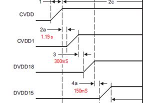
Customer has a product in production that has recently had a few failures in the field. The failures happen during DDR3 memory test when the DSP is at increased temperature (but still within spec: 55-65C). During investigation it has been found that when failure occurred the DSP clock did not switch from 66.6 Mhz to 666 Mhz as it is supposed to during boot which suggests failure with PLL initialization. At this moment the power sequence was closely inspected and it was found that the time between ramping rails is considerably bigger than what's recommended in the datasheet. Actual timing is shown below in red. the question is: could this longer timing between rails cause failure in PLL initialization? 

thanks,Michael

  • Hi Michael,

    I've forwarded this to the DDR experts. Their feedback should be posted here.

    BR
    Tsvetolin Shulev
  • Hi Michael,

    Let me ask a couple more questions.

    1) What is the boot mode used by the customer? Can you share the strapping of the boot mode pins?

    2) The diagram doesn't show the relationship of the power supplies with the  SYSCLK, PORz and the RESETFULLz. Can you include the timing of these signals as well?

    3) When the board does not initialize, has it been determined if the proper bootmode is being initialized? Has the customer checked the DEVSTAT register with an emulator on a failing board?

    The C6657 was not designed for an environment where all the power supplies were not present for long periods of time. We don't know all the effects of prolonged periods of time between the presence of each of the rails but I believe that is more of a long term reliability issue as opposed to a boot issue. That's why I am asking about the timing and relationship between the clock and reset signals. 

    Regards,

    Bill

  • Hi Bill, I'm the board designer that is experiencing the boot problem.  Here are the answers to your questions

    1.  Boot Mode [2:0] = "100" = PCIe

    Boot Mode [8:5] =  Bar Config = 1111

    Boot Mode [9] =  "0" = 100MHz

    Boot Mode [12:10] =  "100" = 156.25MHz

    2.  Here's the full timing diagram with the measured values in red

    DSP measured boot sequence.docx

    3.  No we have not checked this.  Our production boards have the emulator connector no-loaded so we would have solder a connector to a board.

    Thank you for looking into this.

    Heath

  • Hi Heath,

    I see you have your PCIECLK driven by 100MHz and your CORECLK driven by 156.25MHz. Is that correct? Do you have access to the SYSCLKOUT pin? If so, measure the frequency at SYSCLKOUT. It should show the SYSCLK / 6. Check the frequency in both the passing and failing case and see if the failing case shows 26.04MHz. This would indicate that the BOOTROM hasn't configured the system PLL which would be another indication that the bootmode is not latching correctly.
    Regards,
    Bill
  • Hi Bill, we measured 166Mhz on SYSCLKOUT for both a good & failed state so it looks like the main PLL is getting configured.

    I believe we found the problem...  GPIO0 which is also the LENDIAN bootstrap pin has an internal pull-up so we do not pull it up on our board.  Our test board which attaches to our main board just so happens to use GPIO0 and does have a pull-up on it.  Whenever we run with the test board attached, the boot problem never happens no matter how hot the DSP gets.  When we take the test board off, the problem occurs if the DSP is warm/hot but works when cool.  So I believe on some DSP's, the internal pull-up on LENDIAN bootstrap isn't effective when the DSP is above a certain temperature.

    Unfortunately, this will require a board spin. :(

    Heath

  • Hi Heath,

    Section 8.1 and 8.4 of the data manual are pretty clear about the need for external pulls on configuration pins.

    If a configuration pin must be routed out from the device and it is not driven (Hi-Z state), the internal pullup or pulldown (IPU/IPD) resistor should not be relied upon. TI recommends the use of an external pullup or pulldown resistor. For more detailed information on pullup or pulldown resistors and situations in which external pullup or pulldown resistors are required, see Section 8.4.


    The internal pulls are present to hold a pin in a known state if the pin is not used as an output or driven externally. They should only be used to hold unconnected signal balls in a known state. If any external circuitry or trace in attached to the pad on the PCB, an external resistor is needed to ensure that a valid state is present at the input pin. This is doubly true for configuration pins since they will effect the boot state of the device, as you've discovered. 

    Regards,

    Bill

  • Thank you Bill.  Yes we were aware of that requirement.  I think what happened is that originally that pin was a no-connect, but someone at a later time requested an GPIO pin.    So given the volatility of that internal pull-up, is the recommended 20K external pull-up enough?

    Thanks,

    Heath