This thread has been locked.

If you have a related question, please click the "Ask a related question" button in the top right corner. The newly created question will be automatically linked to this question.

6416 PCI Issue

Other Parts Discussed in Thread: TMS320C6416T

Hi Champs:

My customer is having an intermittent PCI issue on 6416. Please see the attached doc file for more information on data being captured..  This is an intermittent problem, and out test (software and hardware) seem to work correctly most of the time.

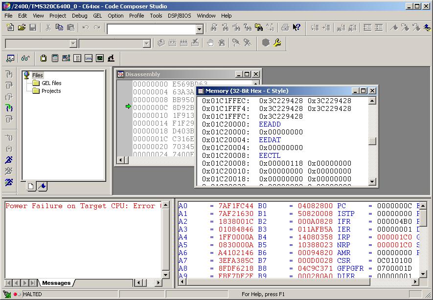
This attached doc  describes a failure condition we see while trying to write to the DSP Internal RAM memory across the PCI bus.  We have only the processor and DSP on the PCI bus.

Thanks for your help.

Pradhyum

FailureDuringRamWriteRead.doc
  • We have auto-initialization disabled, even though there is an EEPROM attached that is unused.  Not sure if this is a problem.

    We cannot seem to readthe HDCR bit from Code Composer.  We have read it from the Host Interface side, but only during sucessfull boots, and it is set.  When I try to read it in CC, I get garbage data (like the attached pic).

    We have only been able to read the HDCR from the Host side, and the PCIBOOT is set.

    I may have been unclear re: resets.  We release the RESET 10 seconds after power up, but long before we attempt any PCI transactions. We allow power and clocks to stablize, then release the DSP and DSP PCI resets, then attempt PCI transactions to it.

    You will notice in the attached pic, that this is following a "release from reset" state.  The PC is non-zero, and I have attempted to read the HDCR address.  I think this is the correct address right?

    Dano

  • yea, I meant we do all of our Gpp memory tests before releasing the DSP from reset.  We do all of our DSP memory tests AFTER reset :)

  • HDCR is only readable from the host.  What value does your GPP read from the HDCR register?

  • We have never programed the PCI Configuration EEPROM with any data.  Our configuration is PCI_EN = 1, MCBSP2_EN = 1, BEA13 = 0.  Will not having the EEPROM programmed, cause any probelms, even through we are technically "disabling" it?

    Do we still need to put something in it even though we are not wanting to use it?

    Can we just remove the part, or is it required to be there?

    -Dano

  • I was wondering about a couple of pins on the DSP. We have a group of pins in the symbol called Resets and Interrupts. It seems like they are in order of interrupt number (INT_0 through INT_7). INT_2 and INT_3 are listed in our symbol as GP0 and GP3. I can’t find anything in the datasheet that actually says that GP0 and GP3 are dual purpose pins. INT 2 and 3 should be non-maskable interrupts. In the datasheet it says they are reserved (in the interrupt table), but in the listing for the GPIO pins, it shows they are used as GPIO, with GP0 able to be configured as an interrupt output. I’ve even looked at spru646a which is the Interrupt Selector Reference Guide and I don’t see any mention of INT_2 and INT_3.


    My question is why are INT_2 and INT_3 reserved and are they muxed with GP0 and GP3?  In this case, we believe we are not driving the pins. The device they are attached to will tri-state the two signals (we don’t have probe access though). However, on another program with a similar design, they are driving GP0 with a 1 and GP3 with a 0. I’m not aware of the reasoning behind that. Would that cause any problems?


    Would there be any configuration register or anything pertaining to these two signals to cause the DSP CPU to come out of the stalled state at power up?

  • My question is why are INT_2 and INT_3 reserved and are they muxed with GP0 and GP3? 

    No INT_2 and INT_3 are reserved and not muxed with GP0 and GP3. INT_2 and INT_3 are probably reserved for some internal use.

    GP0 and GP3 are purely used as GPIO pins. Not all GPIO pins have dedicated CPU interrupts. See SPRU584A GPIO user guide. Pg 13 says that "All GPINTn are synchronization events to the EDMA. Only GPINT0 and GPINT[47] are available as interrupts to the CPU.". The ones that don't have a CPU interrupt will go to EDMA as events and can trigger an EDMA interrupt to the CPU.

    Pradhyum

  • So, we have a new discovery of a possible critical symptom.

    We are seeing the 1st 1k of data in the internal RAM filled with 0xFFFF.  It is almost as though it is coming up in "EMIF Boot" mode.  We tried to veriify this by putting a device onto the EMIF bus, that contains a known data pattern.  However, we do not see this "known data pattern" ending up in the internal memory.

    If we configure the Host Boot pins specifically for "EMIF BOOT", then we DO see the expected EMIF data pattern show up for the 1st 1k of data in the internal SRAM, so we know our theory is correct.  Also, when we attach, we see the Program Counter running other than zero (as expected)

    Something is acting almost like EMIF BOOT, but not quite, because it isn't getting the data from the EMIF bus, but the processor is acting like EMIF boot in ALL OTHER evidences (i.e. 1st 1K of data filled, Program Counter running).

    Our PCI_EN is set to 1.  What does the "reserved boot mode 11" actually do?

    Does this condition sound familiar to anyone?

    Thanks,

    Dano

  • A couple of questions:

    1)  Is there a way the contents of the internal EEPROM (PCI EEPROM) can get transferred to the internal SRAM during a boot?  Is there some Boot Mode that can cause this?

    2) If the EEPROM is blank, will the PCI Config fail?  If so, what happens?  Could a failure to read the PCI EEPROM cause a HPI boot to occur, even if we are not configured for HPI Boot?

    Thanks!

    Dano

  • Dano,

    I wasn't looking at the latest data sheet earlier and mentioned something that was incorrect.  The W25 pin should be connected directly to ground rather than left as a no-connect.  The following errata pertains to this recommendation:

    errata said:

    Power Sequencing − IO Before Core
    If customers are using IO before Core, which was initially supported, it is required to connect the Reserved pin
    W25 to ground due to insufficient pulldown strength. If IO comes up before Core, and W25 is not at ground level,
    this can result in the device coming up in an improper state. To ensure this does not occur, it is required to connect
    W25 to VSS. If this is not done, then the power sequencing must be changed to Core before IO to ensure the
    internal state is set properly.

    Does that errata pertain to you?  Specifically, which power rail comes up first: core or I/O?

    Brad

  • Dano said:

    A couple of questions:

    1)  Is there a way the contents of the internal EEPROM (PCI EEPROM) can get transferred to the internal SRAM during a boot?  Is there some Boot Mode that can cause this?

    2) If the EEPROM is blank, will the PCI Config fail?  If so, what happens?  Could a failure to read the PCI EEPROM cause a HPI boot to occur, even if we are not configured for HPI Boot?

    Thanks!

    Dano

    Can you just probe the EEPROM pins to see if the 6416 is reading from it at power-up?  This would tell us definitively whether we need to care about this.  If the configuration pins were not set correctly and the 6416 was reading from a blank flash then I imagine that could cause issues.  However, given that you have auto-init turned off I don't think this should be the case.

    Brad


  • HI Brad,

    Thanks very much for your support, responses and suggestions.

    • Regarding the I/O before Core. 

    We have looked into this errata in great detail.  At 1st, our I/O was coming up before (or concurrently with) the core, at which time we tried grounding W25.  But we have sinc changed the design so that our Core comes up 160mS before the I/O, and now W25 is no-connect.

    • Regarding EEPROM

    I will probe the EEPROM as you suggested.  My question was more a hypothetical one in that since we suspciously see exactly 1k of data in the SRAM following a power-on reset, I wanted to know all the possible places that exactly 1k could orginate from.  My question was is there any way that the contents of the PCI EEPROM could end up in the SRAM?  I believe the answer to this question is "NO, the PCI EEPROM contents can never end up in the internal SRAM, they are only used for PCI configuration when the DSP is configured to use it."

    We have since written known data to the PCI EEPROM (because it was previously blank), and we are not seeing this known data end up in the SRAM, but still see the FFs there.  We know the FFs are not coming from the EMIFB bus, because we intentionally put drove the EMIF bus, and are not seeing this known data end up in the EEPROM either.  If we intentionally drive the Boot Mode pins for "EMIF BOOT", then we DO see the known EMIF data show up in the internal SRAM.

    I personally have not found in any documentation suggesting any mode that could fill up exactly 1k of data in the internal SRAM except EMIF boot mode.  My thoughts were that perhaps the DSP thinks it is in EMIF Boot Mode (bad or noisey signals or power supplies or whatever reason), but because the DSP is confused, it is unable to get good data from the EMIF bus.  Almost like the Core thinks it's in EMIF boot mode, but the buffers between the Core and the EMIF bus DO NOT, and thus the FFs are being driven when the Core is moving the Data from the EMIF bus to the SRAM.

    -Dan

  • Dano said:
    We are seeing the 1st 1k of data in the internal RAM filled with 0xFFFF.  It is almost as though it is coming up in "EMIF Boot" mode.  We tried to veriify this by putting a device onto the EMIF bus, that contains a known data pattern.  However, we do not see this "known data pattern" ending up in the internal memory.

    This is really interesting behavior.  Can you provide some more details such as:

    • Do the failures/lockups happen on all boards all of the time, some boards all of the time, or all boards some of the time?
    • Does this behavior of seeing all 0xF's correlate perfectly with the failures?
    • Can you probe the EMIF when this happens?  Specifically I'd be curious to see if byte enables are firing, etc.  I wonder if somehow it's trying to boot from a different chip select or something...

    On a related note I received your schematic from Pradhyum.  Can you try setting MCBSP2_EN = 1?

    Brad

  • Thanks again for the feedback.

    Here are some details that may help :)

    1. The failures happen on all of the boards some of the time.  Some boards with more frequency than others. 
      1. Always during the Gpp access to the DSP internal memory. 
      2. Some failures are merely memory test failures, sometimes the failures result in the 'hang condition"
    2. We really are not able to prove or disprove the "0xFs" behavior correlation with the failures.  I think this is because of the timing of the DSP putting the FFs data into the SDRAM and the Gpp putting RAM Test data into the same memory.  Sometimes, we see part of the Gpp RAM Test data overwritten by the FFs, and the FFs can occur at various blocks within the 1k range.  I think this is because the DSP starts writing the FFs data, at the same time the Gpp starts writing pattern data, overwriting some of the FFs data, and at some point, the Gpp writing passes up the DSP moving the FFs data.  Once the Gpp passes up, the DSP overwrites the portion of the Gpp test data pattern beginning at the address where the Gpp passed up the DSP writing.  All of this is a speculation based on our observation of the FFs data in the SDRAM, because sometimes we see the entire 1k filled with FFs, and sometimes we only see portions of the data filled with FFs.  But I don't really know.
    3. Probing the EMIF bus is a challenge for us.  I will see if we can possibly develop a snopper with an FPGA, and maybe get some visibility.  As far as chip selects are concerned, this shouldn't matter, because our FPGA is driving the known pattern on the bus all the time, so it ignores the chip selects.

    Oh, and we have tried setting the MCBSP2_EN bit = 1.  We also changed BE13 to disable auto initialization.  There's a good bet we've tried just about all the pins in all of the possible configurations.  We've poured over the forums and errata's, and even tried some of the ones that apply to Rev1 silicon.

    On a side note, we have several different products using the same Rev2 6416DSP.  They are all using the same basic schematic layout, but power supplies, board stackups and placement of bypass caps do differ.  Some of the different designs show this "hang/ram failure" problem.  1 does not seem to have the problem at all (although we have a much smaller sample size on this design). 

    I always hate to admit it, but I am fairly certain this is our internal design issue, and not a TI DSP issue (simply because one design works), so my questions are more related to solving our internal design issues.  I am hoping that some of the eratic behavior we see, could point you and your experience to something obvious to look at.

    One method we are concurrently persuing is to "sabotage" the "working" design, to attempt to make it fail in the same way (changing supplies, removing filter caps, modifying the configuration, etc.), as another approach to the cause of the problem.

    Thanks again for your help,

    -Dano

  • Dano said:
    My question was is there any way that the contents of the PCI EEPROM could end up in the SRAM?  I believe the answer to this question is "NO, the PCI EEPROM contents can never end up in the internal SRAM, they are only used for PCI configuration when the DSP is configured to use it."

    That is my understanding.  The EEPROM should be irrelevant based on your config pins.

  • Dano said:
    We really are not able to prove or disprove the "0xFs" behavior correlation with the failures.  I think this is because of the timing of the DSP putting the FFs data into the SDRAM and the Gpp putting RAM Test data into the same memory.  Sometimes, we see part of the Gpp RAM Test data overwritten by the FFs, and the FFs can occur at various blocks within the 1k range.  I think this is because the DSP starts writing the FFs data, at the same time the Gpp starts writing pattern data, overwriting some of the FFs data, and at some point, the Gpp writing passes up the DSP moving the FFs data.  Once the Gpp passes up, the DSP overwrites the portion of the Gpp test data pattern beginning at the address where the Gpp passed up the DSP writing.  All of this is a speculation based on our observation of the FFs data in the SDRAM, because sometimes we see the entire 1k filled with FFs, and sometimes we only see portions of the data filled with FFs.  But I don't really know.

    What if you don't do any PCI activity at all?  For example, if you just power up the processor and connect with CCS do you observe PC pointing to some random location?  Can you post a screenshot of the CPU registers and the corresponding disassembly window for this case?

    The other thing you might look at is the EDMA.  We do not have as much visibility into the EDMA as we do in some of the newer devices, but for starters you should try dumping the contents of the parameter RAMS (0x01A00000 - 0x01A007FF), perhaps in a good case and a bad case.

  • Brad,

    Let me know if this contains what you are looking for.  If I stop the PCI access, I can't know for sure if this would be a "PASS" or "FAIL" condition.  I have 2 screen shots here, the 1st shows the PC at zero (which I would expect), and the 2nd shows it non-zero.  Both show the FFs being written.

    It appears, that with the 2nd scenario, that the DSP is executing code (made up of random data), and a thought that we have is that this random running of code could be asserting the "IFRAME" signal on the PCI bus inadvertently (which can cause the Gpp PCI bus to hang).  Interestingly, this signal (IFRAME) serves as an interrupt in some configurations.  Not sure that is a clue.

    I added a 3rd screenshot that shows sometimes not all of the data contains FFs, but some other data.  The data pattern appears repeating, but I don't recognize it.  Maybe you could?

    3348.ScreenShotsWithNoPCIAccess.pdf

    -Dano

  • Another data point (for what it's worth).

    On the design that works, the die has an "A6" in the corner, while on the designs that do not, there is a "1GHz" in the corner.

    Both are running at 1GHz.  The BOM calls out for the 1GHz in both scenarios, so the working ones may have been mispopulated.

    -D

  • Here's another thing I just noticed in the data sheet:

    datasheet said:

    Internal pullup/pulldown resistors also exist on the non-configuration pins on the BEA bus (BEA[12, 10, 6:1]).
    Do not oppose the internal pullup/pulldown resistors on these non-configuration pins with external
    pullup/pulldown resistors. If an external controller provides signals to these non-configuration pins, these
    signals must be driven to the default state of the pins at reset, or not be driven at all.

    Do you know if you meet this requirement?  The BEA[n] pins are very critical in the device coming up in the correct state.  Since this issue seems to be dragging out a bit perhaps you might consider performing a test where no other devices are populated on the EMIF.  Then you can see if the CPU still points to random locations when you power up the device.  Alternatively you could put a logic analyzer on every single pin so we can verify the logic levels.  Be careful with the trigger levels, i.e. we don't want to think something is a '0' but have the DSP interpret as '1'.

  • Hi Brad,

    We do meet this requirement.  We have carefully looked at each of the BEA pins before, during, and after reset, to make sure they were at the correct levels during release of reset.  We have also tried completly tri-stating all of the EMIF bus from the FPGA by holding it in reset, and also by not loading an image into it.  Our FPGA designer insures me this will tri-state the bus.

    -Dan

  •  

    In the data sheet page 137, the P/N TMS320C6416TGLZ (1GHZ) is shown as obsolete, while TMS320C6416TBGLZ (1GHZ) is shown as active.  Page 64 there is no mention of the "B" field in the nomenclature desciption.

    The marking on the part that we are using does not have the "B".

    Can you ellaborate on this descrepancy?

    Thanks,

    Dano

  • I was confused by the same thing a while back.  The 'B' is part of the orderable part number, but not part of the package markings.  For example, here's a package marking:

    TMS320C6416TGLZ
    D20 -73AFVRW

    The "D20" indicates this is Rev 2.0 silicon, i.e. it's a 6416TB.

  • Thanks,

    What does the $N20 indicate?  We see this rather than the D20 on both the 1GHZ and the A6 parts.

  •  It's the "20" that we care about.  That means Rev 2.0.  The other option would be "10" which was Revision 1.0.

  • Here's our "A6".  We dont' have a pic of the 1GHZ,  but the only differences are that the "A6" is replaced with "1GHZ" and the other line conaines a "$N20-94A535W"


  • Are you able to put one of the 600 MHz devices on this design (perhaps changing the PLL setting to match)?  That might serve as a good data point.  In other words, the 600 MHz devices and 1 GHz devices are on separate ends of the process curve.  If the 600 MHz devices seem to boot ok that would indicate to me that something on your board is not quite in spec, causing it to work on one end of the process but not the other.  When all the specs are met it will work reliably across process, temperature, etc.

  • Changing the processor is not an easy feat.

    I did just get some new data from the group that designed around the A6 though, and they started seeing the same failure during PCI access to the DSP.  They started seeing the problem running at elevated temperatures, and are now seeing it on one board, even on the bench at room temperature.

    We have been looking at the evaluation board a little also.  There, when we configure for PCI boot mode, we do see the PC not always at zero, but sometimes at 0x00000018 and sometimes at 0x00000024.  We see random data in the SRAM (and not FFs), which is what I expect.  I did expect to see the PC at zero every time though, so this gives me a clue what to expect.  But in no case, did I see the PC way out far away from zero, like I see often in our designs.

    -Dano

  • Any updates?  Another idea that came to mind was to see if you can reproduce this behavior on the EVM.

  • Dan:

    As I mentioned to you , Here are some things to check..

    -          Slow down the processor to 600 MHz and see if you are seeing fewer instances of lockup

    -          Reproduce problem on EVM - So that we can see whether it is an issue specific to your board or something to do with the chip

    -          Check JTAG circuitry as per the link below

    http://processors.wiki.ti.com/index.php/XDS_Target_Connection_Guide#Target_Connection_Design

    Thanks,

    Pradhyum

  • Slowing down to 600 MHz has no affect.

    The JTAG circuitry looks fine as well.

    We are not able to duplicate the problem on the EVM.  We have configured the EVM to PCI Boot Mode, and wired it directly into our design, and are holding OUR DSP in reset, thereby using the EVM DSP via PCI from our Gpp.  Everything seems to work correctly.

    Some differences:

    • The EVM is power sequenced differently and seperately
    • The EVM has a different LOT code on the DSP
    • The EVM must be powered prior to our design, or it hangs up.

    We now see the failure on our 3rd in-house design.  Orginally, we didn't, but temperature stressing the board, and stressing the clocking seems to be introducing failures on that design as well.

    Q:  Could NOT driving RESET to the DSP during the initial board bring-up, or perhaps driving it incorrectly, cause permant damage to the DSP part?  Since we drive these resets from a CPLD, and the initial board bring-up process does not include a programmed CPLD, we are wondering if invalid signals on either the RESET to the DSP or any other mode pins, could cause some permanent damage to the DSP.

    Thanks,

    Dano

  • Dano said:
    Q:  Could NOT driving RESET to the DSP during the initial board bring-up, or perhaps driving it incorrectly, cause permant damage to the DSP part?  Since we drive these resets from a CPLD, and the initial board bring-up process does not include a programmed CPLD, we are wondering if invalid signals on either the RESET to the DSP or any other mode pins, could cause some permanent damage to the DSP.

    The main way to damage the device would be to apply voltage to pins (like nRESET) when the device is not powered.  Here's the relevant spec that would violate:

    If the device is not powered then DVdd = 0.0V and so you cannot apply more than 0.5V to a pin.

    Do you think that's an issue?  Can you elaborate more on what is or isn't happening to the RESET pin?


  • I don' think we are at risk of driving the signals before voltage is ramped up.  We read an errata applicable to older dies, that indicated that RESET should be driven LOW during power RAMP-UP, or internal fuses could be blown, causing permanent damage.

    We wondered if this could be an issue.

    For our boards, when we power up, RESET isn't driven LOW until after the Vcc is ramped up (becaus the CPLD driving RESET active hasn't come up).  So essentially, the DSP will see power, then RESET will be asserted until all of the clocks are stable, etc.  Some time later, RESET will be deasserted, allowing things to come up.  Our solution was to put a pull-down resistor on the RESET signal.

    We have wondered of this "floating" state of the RESET signal during power-up could have caused permanent damage to the DSP.

    Thanks,

    Dan

  • Dano said:
    We read an errata applicable to older dies, that indicated that RESET should be driven LOW during power RAMP-UP, or internal fuses could be blown, causing permanent damage.

    That errata applies to the 6416 Rev 1.02 and earlier.  You are using a different device altogether (not just different revision), 6416T Rev 2.0.

  • I'm concerned about your power supply decoupling.  Can you swap some of the caps on your board?  We recommend the following in the data sheet:

    • 560 pF caps closest to the device
    • 220 nF caps next closest
    • 100 uF caps can be further away (4 per supply)

    When reset is released I assume that will cause a current inrush.  Without proper power supply decoupling that could cause a momentary supply dip which might cause "funny things" to happen.

    Brad

  • Dan:

    Any updates since Brad's last post ?.

    Thanks

    Pradhyum

  • There has been no further progress.  None of the recommendations have helped yet.

  • I happened to look at the 6416 to 6416T Migration Guide and noticed something interesting in the Reset chapter:

    • "The device will not be fully out of reset and initialized until after the 16070P (P=1/CPU) delay, and the host boot should not proceed until the 16070P delay has elapsed."

    After releasing reset does your host wait for 16070 CPU cycles before doing any accesses?

    What testing did you do in terms of power supply decoupling?  Were you able to put 560pF caps on?  Which size?  How close?