This thread has been locked.

If you have a related question, please click the "Ask a related question" button in the top right corner. The newly created question will be automatically linked to this question.

TMS320C6678: SPI Booting and DDR initialization Problem

Expert 6030 points
Part Number: TMS320C6678

Team,

On our board the C6678 DSP works in memory boot mode. We gonna use the SPI flash as a boot source - avoiding the IBL usage. We've followed to http://processors.wiki.ti.com/index.php/File:C6678_directROM_boot_examples.zip steps to generate the SPI image and programmed it directly to SPI flash via an external programmer and soldered down the flash memory to our board. After it the DSP ROM boot loader successfully configures the device resources to start the boot process, loads the image from SPI flash into the device and stuck on RBL hand-over process so it still doesn't execute the image.

Next I tried to program the SPI flash via the C6678 DSP as described in manual. I used CCS and C:\ti\ccsv5\ccs_base\emulation\boards\evmc6678l\gel\evm6678l.gel as our board's .gel file to connect to our board but the .gel file did not match to our board, DDR3 test failed and the console gave next output:

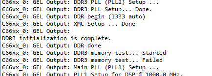
At test time the DSP reads different values that it wrote before.

I tried to reconfigure the .gel file according to the SDRAM part's datasheet (since it differs from C6678 EVM's part) and the geometrical/timing specifications as described in the http://www.ti.com/lit/an/sprabl2e/sprabl2e.pdf KeyStone I DDR3 Initialization manual via the spreadsheets mentioned in this application report but have no success yet.

Could you please describe the most critical steps in this manual to let me correct the .gel file and mention the needed sources for you in case if we decide to ask you for .gel file calculation for our board on your side.

P.S.

​Next are the core schematics differences between our board and TI's C6678 EVM reference board regarding to DDR3 memory controller:

  • On our board the DDRSLRATE0 and DDRSLRATE1 channels are pulled down both with the 0 Om resistors (1 KOm pull up resistors are not loaded) while in the C6678 EVM the DDRSLRATE0 is pulled down with the 2 KOm resistor and the DDRSLRATE1 is pulled up with the 2 KOm
  • ​The SDRAM parts used​​ on our board is MT41K1G8SN-125 while the C6678 EVM uses K4B2G1646C-HCH9​​. We configured the DDR3 controller at 666.67MHz because of the errata on C6678 silicon but SDRAM part on our board is 800MHz speed grade part
  • DDRAM fly-by problem. 

- This note is from the EVM: Address/Command/Control/Clock routing must be Fly-By in byte order 0, 1, 2, 3 ECC, 4, 5, 6, 7. 

- Our board's order is 0,1,2,3,ECC,7,6,5,4​ so how read and write leveling handles this?

​Please take a look to this and let us know in case if these differences can cause the above mentioned test failure.  Additional questions:

  • Still I can't understand why the DSP RBL stuck on hand-over process and doesn't execute the loaded image at first experiment when we write the SPI flash via the programmer
  • Can we execute some instructions on DSP directly via JTAG interface without SPI flash and DRAM interaction?
  • I've forwarded your query to the software experts. Their feedback should be posted here.

    BR
    Tsvetolin Shulev
  • PM,

    We recommend that you break your issue into 2 different parts. The first one is a DDR initialization issue and the second issue relates to Booting directly from SPI as these are questions for 2 different set of experts.

    I will respond the the SPI boot questions and then loop in the DDR experts to help with the other issue.  Can you indicate, if you have tried the SPI boot example and validated on the TI EVM before trying it on the custom design.  Are you using TI flashing utilities or your own programmer to program the flash. this is important as you need to get the byte ordering correct when programming the flash. Is the boot image, you are using also initializing DDR and then trying to load image into DDR memory ?  Can you provide a log of the Debug GEL file after the boot fails (Can you provide this log) ? Have you checked that the bootmode in DEVSTAT matches how these pins are configured on the custom board?  Before determining why the RBL doesn`t pass control, Can you confirm the application code and data sections are loaded in memory (Check memory map and try to load the symbols from the application .out)

    Regards,

    Rahul

  • PM,

    As Rahul said, this problem needs to be broken into 2 parts.  You should work to get the DDR configured correctly and operating robustly independent of the getting the compiled boot solutions functional.  I recommend that you get the DDR interface configured and functional simply using the GEL file with CCS connected to your board with a JTAG debugger. 

    DDR commissioning is also in 2 parts: proper board design and proper software configuration.  The DDR Layout Guidelines must be followed to obtain a properly routed board.  Then the steps in the DDR Initialization Guide must be followed to get the DDR Controller and PHY properly configured to communicate robustly with the DDR3 SDRAM.  Please refer to the steps outlined in this other E2E post to complete the layout and commissioning steps e2e.ti.com/.../462229 .

    Tom

  • Rahul, please find answers point by point for your questions:

    • I'm not able to try / validate the SPI boot example on TI C6678 EVM since simply we don't have the EVM and we've designed our board exclusively based on C6678 hardware reference manuals
    • We use own programmer to program the SPI NOR flash and the SPI fetching passes well from start to end but doesn't execute the image after fetching, which means there can't be the byte-swapping problem (in other case the fetch process had been broken as well)
    • We still can't execute the image built exactly on the way described in C6678 directROM boot example (processors.wiki.ti.com/.../File:C6678_directROM_boot_examples.zip) which doesn't initialize the DDR A.F.A.I.K.
    • I don't see any output on CCS console after I switch the evmc6678l.gel with the Shannon_SystemDebug_v0.4.gel file from start to the end of target connect -> nor_writer.out load to CCS -> app.dat load to 0x80000000 address flow till the nor_writer.out execution when I see just "[C66xx_0] NOR Writer Utility Version 01.00.00.03" CCS console output (the last can be a result of difference between SPI flashes used on C6678 EVM and ours - we use MICRON_S25FL128S instead of NUMONYX_N25Q128A11BSF40F used on EVM)
    • The bootmode in DEVSTAT is set to ROM SPI boot  - so it should be good for this side
    • The memory is not initialized properly (the dram test fails) so the application code and data sections load aren't / can't be correct

  • Hi Everybody,

    I am talking behalf of Andranik too.
    We were able to fix all issues and looks like we don't have any problem at this moment.
    Our customized board could boot up from the SPI flash and send out the Hello world message on the serial output.

    The main problem was DRAM settings everywhere. It was bad in the gel file, in the pdk library and the pre-complied LED demo, what we pre-programmed in the flash chip. The norwriter uses the same library, writing the image to the flash failed too. Also we use a different SPI flash than the EVM, I have to customize the norwriter to make it work after the DDR got fixed.

    Since the DRAM test was not error free, every single program what we tried exited the main() function before it was able to do anything useful. It didn't show any error message on the console....

    Anyway, thank you for your support with these problems.

    Thanks you,
    Robert
  • Thanks for the update Robert and good to hear. I'll mark the thread as answered.

    Phil