This thread has been locked.

If you have a related question, please click the "Ask a related question" button in the top right corner. The newly created question will be automatically linked to this question.

AM5728: GPMC read latency

Part Number: AM5728

Hi,

Depending on the number of executions of the code, GPMC read access is affected.
GPMC register is set as follows.

GPMC_CONFIG1_i 0x60 0x00601211
GPMC_CONFIG2_i 0x64 0x00090902
GPMC_CONFIG3_i 0x68 0x00010100
GPMC_CONFIG4_i 0x6C 0x06030903
GPMC_CONFIG5_i 0x70 0x00090A0A
GPMC_CONFIG6_i 0x74 0x86020281
GPMC_CONFIG7_i 0x78 0x00000F42

During GPMC read access,
When cortexA15 executes more than 40 instructions, 170ns delay occurs with GPMC access.
Why does this delay occur?
Please tell me how to solve the delay.

①call_16_read:
call_16_read:

ldrh r10, [r0] /* r0 = address on GMPC LSC0 */
ldrh r10, [r0]
ldrh r10, [r0]
ldrh r10, [r0]
ldrh r10, [r0]
ldrh r10, [r0]
ldrh r10, [r0]
ldrh r10, [r0]
ldrh r10, [r0]
ldrh r10, [r0]
bx lr

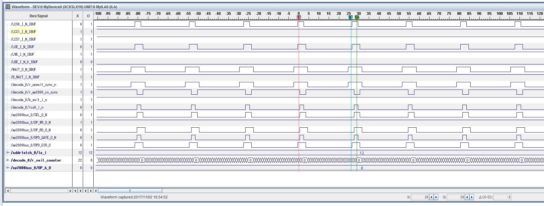
no instructions between gpmc reads -> no delay
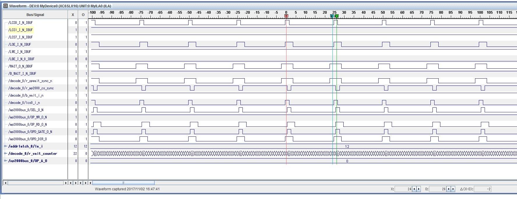
②call_16_read20:

ldrh r10, [r0] /* r0 = address on GMPC LSC0 */

ldrh r9, [r1] /* r1 = address on stack (will be in cach) */
ldrh r9, [r1]
ldrh r9, [r1]
ldrh r9, [r1]
ldrh r9, [r1]
ldrh r9, [r1]
ldrh r9, [r1]
ldrh r9, [r1]
ldrh r9, [r1]
ldrh r9, [r1]

ldrh r9, [r1]
ldrh r9, [r1]
ldrh r9, [r1]
ldrh r9, [r1]
ldrh r9, [r1]
ldrh r9, [r1]
ldrh r9, [r1]
ldrh r9, [r1]
ldrh r9, [r1]
ldrh r9, [r1]


ldrh r10, [r0] /* r0 = address on GMPC LSC0 */
ldrh r10, [r0]
ldrh r10, [r0]
ldrh r10, [r0]
ldrh r10, [r0]
ldrh r10, [r0]
ldrh r10, [r0]
ldrh r10, [r0]
ldrh r10, [r0]
bx lr

Added 20 lines of instructions between gpmc reads -> no delay between accesses of added code
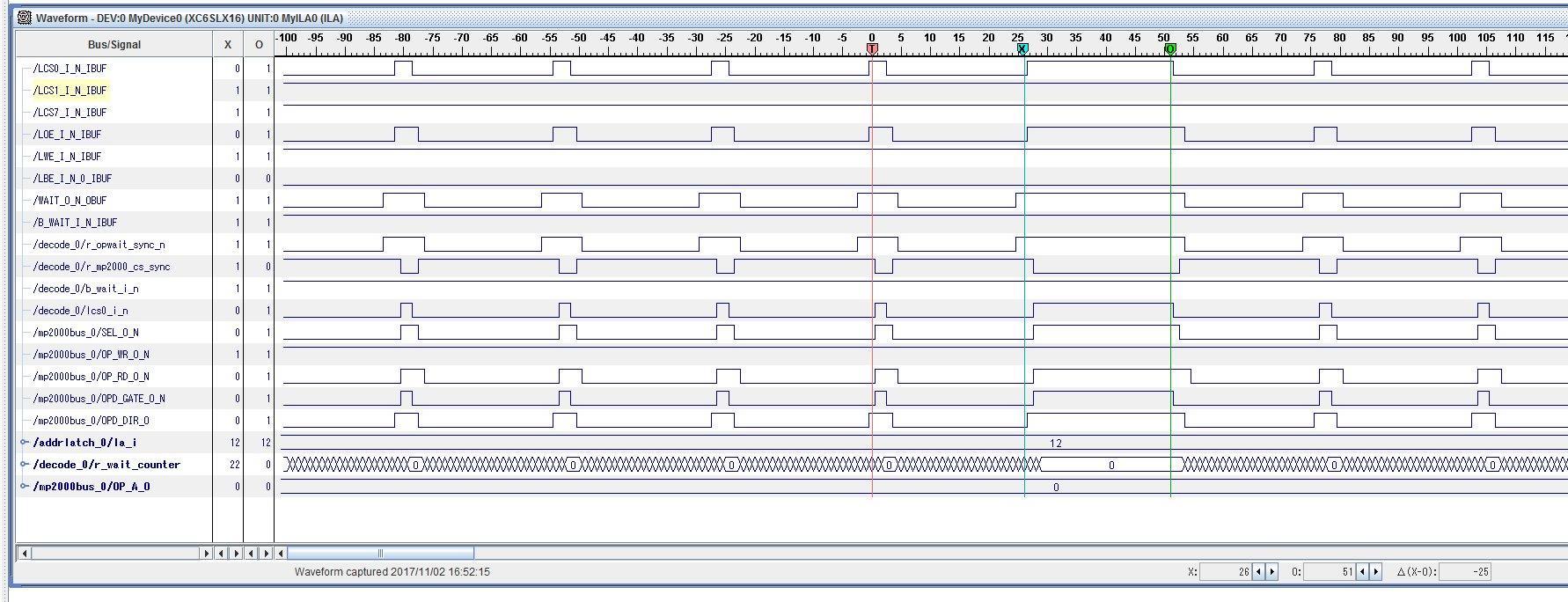
③call_16_read40:

call_16_read40:

ldrh r10, [r0] /* r0 = address on GMPC LSC0 */

ldrh r9, [r1] /* r1 = address on stack (will be in cach) */
ldrh r9, [r1]
ldrh r9, [r1]
ldrh r9, [r1]
ldrh r9, [r1]
ldrh r9, [r1]
ldrh r9, [r1]
ldrh r9, [r1]
ldrh r9, [r1]
ldrh r9, [r1]

ldrh r9, [r1]
ldrh r9, [r1]
ldrh r9, [r1]
ldrh r9, [r1]
ldrh r9, [r1]
ldrh r9, [r1]
ldrh r9, [r1]
ldrh r9, [r1]
ldrh r9, [r1]
ldrh r9, [r1]

ldrh r9, [r1]
ldrh r9, [r1]
ldrh r9, [r1]
ldrh r9, [r1]
ldrh r9, [r1]
ldrh r9, [r1]
ldrh r9, [r1]
ldrh r9, [r1]
ldrh r9, [r1]
ldrh r9, [r1]

ldrh r9, [r1]
ldrh r9, [r1]
ldrh r9, [r1]
ldrh r9, [r1]
ldrh r9, [r1]
ldrh r9, [r1]
ldrh r9, [r1]
ldrh r9, [r1]
ldrh r9, [r1]
ldrh r9, [r1]

ldrh r10, [r0] /* r0 = address on GMPC LSC0 */
ldrh r10, [r0]
ldrh r10, [r0]
ldrh r10, [r0]
ldrh r10, [r0]
ldrh r10, [r0]
ldrh r10, [r0]
ldrh r10, [r0]
ldrh r10, [r0]
bx lr

Added 40 lines of instructions between gpmc reads -> 170ns delay between accesses of added code

Best Regards,
Shigehiro Tsuda

  • Biser,

    This is a test assembly code written by customer. I'm checking processor initialization code used by customer.
  • Tsuda-san,

    Please see suggestions in these forum threads.
    e2e.ti.com/.../43106
    e2e.ti.com/.../176382
  • Hi Shin-san,

    Thank you for quick reply.

    Our customers seems that most of their applications are single-access GPMC.
    Therefore it is not to use the burst access and DMA and NEON.

    The introduction thread seems to recommend using DMA, so it seems to be different from this problem.
    Depending on the amount of code, delay in GPMC access is a problem.
    Is there any other information?

    Best Regards,
    Shigehiro Tsuda

  • Tsuda-san,

    We have recently added GPMC driver support for Sitara device AM335x and AM437x in Processor SDK RTOS.

    I am providing a code snippet of RTOS configuration for access parallel NOR that you can use as reference ( AM355x configuration is provided below)

    Cache MMU settings on the ARM for your reference:

    /* ================ Cache and MMU configuration ================ */
    
    var Cache = xdc.useModule('ti.sysbios.family.arm.a9.Cache');
    Cache.enableCache = true;
    Cache.configureL2Sram = false;//DDR build
    
    var Mmu = xdc.useModule('ti.sysbios.family.arm.a8.Mmu');
    Mmu.enableMMU = true;
    
    /* Force peripheral section to be NON cacheable strongly-ordered memory */
    var peripheralAttrs = {
        type : Mmu.FirstLevelDesc_SECTION, // SECTION descriptor
        tex: 0,
        bufferable : false,                // bufferable
        cacheable  : false,                // cacheable
        shareable  : false,                // shareable
        noexecute  : true,                 // not executable
    };
    
    /* Define the base address of the 1 Meg page the peripheral resides in. */
    var norBaseAddr1 = 0x08000000;
    
    /* Configure the corresponding MMU page descriptor accordingly */
    Mmu.setFirstLevelDescMeta(norBaseAddr1,
                              norBaseAddr1,
                              peripheralAttrs);                                                      
    
    /* Define the base address of the 1 Meg page the peripheral resides in. */
    /* var norBaseAddr2 = 0x09100000; */
    var norBaseAddr2 = 0x08100000;
    
    /* Configure the corresponding MMU page descriptor accordingly */
    Mmu.setFirstLevelDescMeta(norBaseAddr2,
                              norBaseAddr2,
                              peripheralAttrs);    
    
    /* Define the base address of the 1 Meg page the peripheral resides in. */
    var gpmcBaseAddr = 0x50000000;
    
    /* Configure the corresponding MMU page descriptor accordingly */
    Mmu.setFirstLevelDescMeta(gpmcBaseAddr,
                              gpmcBaseAddr,
                              peripheralAttrs);                                                      
    

    Hope this helps.

    Regards,

    Rahul

  • Since AM572x has A15 core, you can refer to the following discussion between Stuart and Eric for setting up the MMU for GPMC access:

    e2e.ti.com/.../592105

    Regards,
    Rahul
  • Tsuda-san,

    For your reference, this is a very good wiki article discussing this topic.
    processors.wiki.ti.com/.../Common_Issue_Resulting_in_Slow_External_Memory_Performance
  • Hi Shin-san,

    Thank you for quick reply.

    If there is a lot of single access to FPGA and they want to realize as fast access as possible, which of the following should be better for GPMC?
    1. Set as cache area
    2. Set as non-cacheable area

    In the case of Rahul-san's answer NOR flash setting, it seems that it is set as non-cache and strongly-ordered memory area.

    The wiki site of your introduction has the following description.
    · Set as cache area
    · Using multiple load instructions

    Best Regards,
    Shigehiro Tsuda

  • Tsuda-san,

    If the FPGA memory space accessible by GPMC can be only changed by AM5728 (i.e. the data doesn't change by FPGA activity), the GPMC memory space for FPGA should be set to casheable. Otherwise, it should be set to non-casheable.