

Hi All,
I would like to ask a group of related questions on VPFE:
First is an erratic behavior I observed with FLDSTAT bit of register SYN_MODE in VPFE.
According to the document SPRU977a, 643x VPFE User's Guide, page 126, table 58 "Sync and Mode Set Register (SYN_MODE) Field Descriptions", FLDSTAT serves as field indicator:

Because in BT.656 mode field 0 and 1 comes alternatively in the stream, and it seems that according to the document, if we have an interrupt service routine being triggered by VD associated with the beginning of each field, we should be able to see the toggling between 0 and 1 every time we entering the interrupt service routine.
But in my experiment, in which I have made the ISR triggered by VDINT0 to be very short to avoid any possible complication due to nested ISR, although I do observe change in FLDSTAT, it is NOT regular. At most times it does NOT toggle as expected at new field (I watch SYN_MODE value in breakpoint within ISR), but could remain at either 1 or 0 for several fields before changing to another. For example, the observed pattern of FLDSTAT between consecutive fields could be like:
11110001111011101

This is recorded by reading and then saving the value of SYN_MODE to an entry in a global static integer array, incrementing the index at every ISR (triggered by VDINT0) by one. static int i=0; interrupt void my_isr() It clearly does NOT look like a field indicator whose pattern of change should be ...1010101010... But even with this fairly long delay, which is to provide enough time if the SYN_MODE.FLDSTAT bit do need time to update after VD, I still observe the same erratic FLDSTAT changing pattern as with very short (in fact 0) VPFE_CCDC_VDINT value. Why does this happen? Did I miss anything in the setting or have made any mistake in reading SYN_MODE? What exactly does VPFE work for BT.656 stream? VPFE has a SDOFST register which can be conveniently configured to do the de-interlacing, but what is its internal mechanism?
I wish to have get an answer on these VPFE mechanism questions. There are still a few remaining questions: from http://en.wikipedia.org/wiki/Interlace And I also could not understand why VPFE provide both VDINT0 and VDINT1. For the same VD event (two VDs for a BT.656 frame), why two interrupts are needed? (SPRU977a, page 89) In what aspects are these interrupts "different"? Sincerely,
static int field[50];
{
i++;
field[i%50]= VPFE_CCDC_SYN_MODE; //VPFE_CCDC_SYN_MODE points to address 0x01C70408 in my 6437
}
I thought on whether it was because this my_isr() executes too fast, immediately following VD so that when my_isr() is reading SYN_MODE, SYN_MODE it has not yet been updated according to the ID of the new (current coming-in) field. To avoid this I tried to change the value VDINT0 delay after VD.
VPFE_CCDC_VDINT = 0x00300030; //made both VDINT0 and VDINT1 happen 48+1 (please see page 140, SPRU977a on why there is a "+1") lines after VD, which I think it quite long
My objective of reading FLDSTAT is to determine from which field the current interrupt is coming from. Digital cameras nowadays capture a whole frame once at a time and only split it to two fields to accommodate BT.656 standard which was intially designed for degital conversion of analog TV signals. Therefore, top (field 0) and bottom (field 1) fields needs to be combined to restore the original frame. 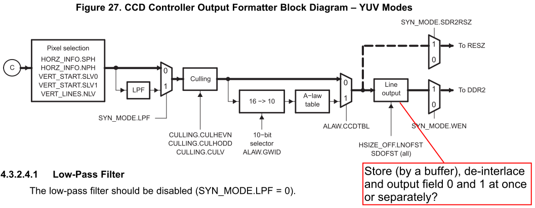
( page 55, SPRU977a)
According to Figure 27. CCD Controller Output Formatter Block Diagram – YUV Modes, Line output is the last stage in the pipeline. Does VPFE
2) Or does it has an internal buffer to store all lines within in a field first and then output them separetely?
3) I don't think in 2) outputting a whole field as an integral block directly to DDR2 is possible. This is due to the interlacing nature of BT.656 such that field 0 and 1 has one line's shift between corresponding lines, so any attempt to write a field as a whole block will overwrite most of the contents of another field.
Although BT.656 has embedded FVH bits to as the field ID, how can we get it in VPFE? I have tried to read SYN_MODE.FLDSTAT which is only relevant register I could find in VPFE's document (SPRU977a), yet using it is not successful. If I am not able to determine after which field and ISR (triggered by VDINT0) is from, how do I know that the content in the the DDR2 memory output by VPFE is not a "mixed" frame with field 1 from the previous frame and field 0 from the current frame? In digital cameras these two fields are taken at different time and there could possibly be "interlacing artifact" due to the incorrect combination.
It is therefore not only necessary, but imperative to know the field ID to determine the proper action in an ISR triggered by VDINT0. How can I know this?
Zheng


