This thread has been locked.

If you have a related question, please click the "Ask a related question" button in the top right corner. The newly created question will be automatically linked to this question.

Linux/AM5718: Clock noise

Part Number: AM5718
Other Parts Discussed in Thread: TMDXIDK5718

Tool/software: Linux

Hi.

My customers made a custom board referring to TMDXIDK 5718.
We want to check SYS_CLK1 from clkoutx.
(TRM: See Figure 3-36, 37)

I set the following registers with TMDXIDK 5718,
the clock could not be confirmed from clkout3.

1. CTRL_CORE_PAD_XREF_CLK3
2. CTRL_CORE_PAD_XREF_CLK0
3. CM_IPU_TIMER5_CLKCTRL
4. CM_IPU_TIMER6_CLKCTRL
5. CM_IPU_TIMER7_CLKCTRL
6. CM_IPU_TIMER8_CLKCTRL
7. CTRL_CORE_HWOBS_CONTROL

devmem2 0x4a003694 w 0x00000009
devmem2 0x4a005558 w 0x0B000000
devmem2 0x4a005560 w 0x0B000000
devmem2 0x4a005568 w 0x0B000000
devmem2 0x4a005570 w 0x0B000000
devmem2 0x4a002360 w 0x00000001

(example)
root@am57xx-evm:~# devmem2 0x4a0036a0 w 0x00000009
/dev/mem opened.
Memory mapped at address 0xb6f9b000.
Read at address 0x4A0036A0 (0xb6f9b6a0): 0x00050009
Write at address 0x4A0036A0 (0xb6f9b6a0): 0x00000009, readback 0x00000009
009

Question 1:
Would you tell me the register setting required to check SYS_CLK1 from clkout3.

Question 2:
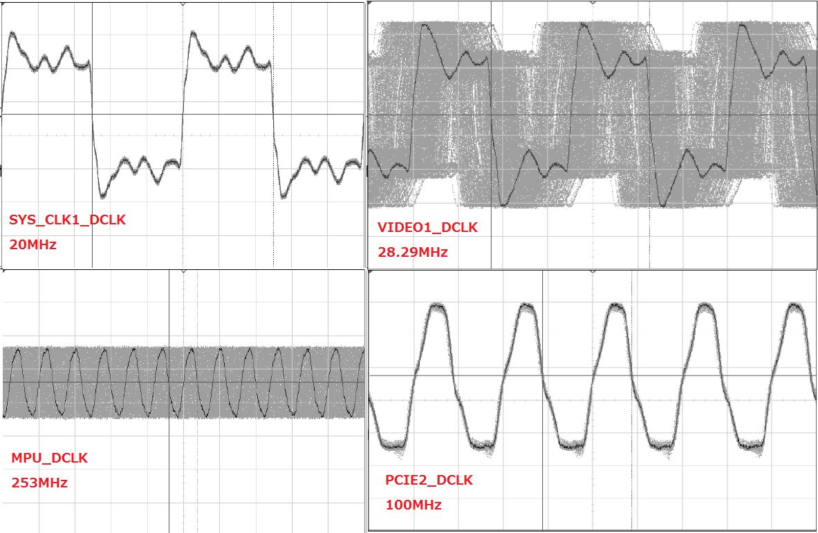
My customers could to confirm SYS_CLK1 from clkout2.
When they confirmed SYSCLK from clkout2, they could confirm a beautiful waveform.
However, if you check MPU_DCLK or VIDEO1_DCLK, the waveform is distorted.
The power supply has no noise and can not find causes.
Are there any possible causes?

Wave information


Regards,
Rei

  • Rei,

    #1  I recommend that you use the Pinmux tool.  It will work out all of the register values and help you avoid conflicts.  The pinmux file for the TMDXIDK5718 is distributed as part of ProcSDK under the pdk directory tree.  The pinmux tool is available at http://www.ti.com/tool/PINMUXTOOL .

    #2  The clock waveform captures do not have enough information to determine "goodness".  Vertical deflection, ground reference and timebase are minimum requirements.  Note that the clkout# outputs are LVCMOS drivers so that are bandwidth limited at about 200MHz.  The amplitude will be restricted as you approach the limit.  Also note that these clkout2 and clkout3 outputs have limited use as shown in the notes in Section 4.4.26 of the Data Manual.  They are not intended as high performance clocks used to drive other circuitry.

    Tom

  • Hi Tom,
    #1
    I recommend Pinmux tool to my customers.
    Thank you for teaching it.

    #2
    Sorry, my explanation was missing.
    Please check the uploaded pdf file.

    wave_for_e2e.pdf

    Do you have any advice?

    Regards,
    Rei

  • Rei,

    I do not see anything in these scope shots that is problematic.

    1. SYS_CLK1_DCLK appears to be an unterminated  20MHz output.  Transition edges are clean and the overshoot and undershoot do not violate VOH(min) or VOL(max)
    2. MPU_DCLK is a 250MHz clock.  Since it is beyond the frequency range of the LVCMOS buffer, the amplitude is reduced and the signal never reaches the expected LVCMOS voltage limits.  The trigger delay shows that this clock has period jitter but that is not unexpected.
    3. VIDEO1_DCLK is about 28MHz with signal integrity like #1.  The trigger delay shows that this clock has period jitter but that is not unexpected.
    4. PCIE2_DCLK is a 100MHz clock.  Since it has lower frequency than #2, you can see that it reaches the voltage rails as expected.  You also see that there is almost no phase jitter as a PCIe reference clock must be a low-jitter clock.

    Please let me know if you have further questions.

    Tom

  • Hi Tom,
    I appreciate your information.

    ///
    3. VIDEO1_DCLK is about 28MHz with signal integrity like #1. The trigger delay shows that this clock has period jitter but that is not unexpected.
    ///

    Question 1:
    What do you mean " that is not unexpected" ?

    We think that clock jitter is bad. We have questions related to the above.
    We measured the VOUT1_HSYNC on TMDXIDK5718. However, we checked the clock jitter.

    hsync.pdf

    Question 2:
    Would you tell me the register settings to avoid clock jitter.

    Regards,
    Rei

  • Rei,

    Digital circuits are not affected by clock period jitter as long as it is bounded and never violates minimum set-up and hold requirements within the logic.  PLLs that only use integer multipliers and dividers will yield the lowest jitter but that will place unacceptable limits on system performance.  As long as you follow the guidelines provided, the clock period jitter will not cause a problem within the device.  If you want to use the clock external to the device, signal conditioning may be needed.  As stated in the Data Manual, these clkout# outputs can be used externally for devices with noncritical timing requirements, only.

    Tom

  • Hi Tom,
    Thank you for your reply.

    We understand that clkout# is not good.
    (It is only used to observe the clock.)
    Now my customers are using vout1_xxx (Figure 11-2 in TRM).

    The following signals were confirmed to be operating within the specified range for setup and hold.
    ・vout1_clk,
    ・vout1_d[23:0],
    ・vout1_hsync
    ・vout1_vsync

    Question 1:
    We are concerned about the clock period jitter on IDK of vout1_clk and vout1_hsync.
    Is this happening because spread spectrum is enabled?

    Question 2:

    I want to output DPLL_HDMI to vout1_clk. (not DPLL_VIDEO1)
    Because I thought that clock period jitter would be improved.
    What register settings can we output DPLL_HDMI to vout1_clk?

    Regards,

    Rei

  • Rei,

    The VOUT interface does support SSC clocking.  This allows for the radiated noise from this interface to have its spectrum flattened to help pass compliance tests.  Control for the SSC modulation is through the software.  I do not know if it is enabled by default or not.

    Figure 11-4 in TRM section 11.1.2.1 shows the DSS subsystem clock multiplexers.  Table 11-7 that lists the clock options for muxes 1, 2 3 and 10.  The 3rd note under the table points to the register that has the control for muxes A, B and C.  Mux A is the one needed to select the HDMI clock.  DSI1_A_CLK1_SELECTION is bits [4:3] in the DSS_PLL_CONTROL register shown in Table 18-292 CTRL_CORE_DSS_PLL_CONTROL on page 4265.

    Tom