This thread has been locked.

If you have a related question, please click the "Ask a related question" button in the top right corner. The newly created question will be automatically linked to this question.

AM3351: DDR2 JEDEC compliance issues

Part Number: AM3351


Hi!

It has been a while on the DDR2 topic, before our equipment was not good and also time was limited to analyze in-depth, but lately we have had time to measure integrity and timing of the DDR2. The previous question about the Vswing is not applicable anymore, we solved the amplitude with an parallel termination on the clock differential and series termination. (Not sure why this is not added in the datasheet as a requirement on the differential clock to the DDR2 device.)

Now we almost finalized the qualification successfully but we run into a few points which are not okay yet. (Below the measurement I'll share details about the design).

1.  When measuring read bursts timing fails on:

- tAC-Diff, CK, DQ which is required to be +/- 500 ps. Measurement results show between -628.75 ps and -282.71 ps.

Histogram hits tAC-Diff

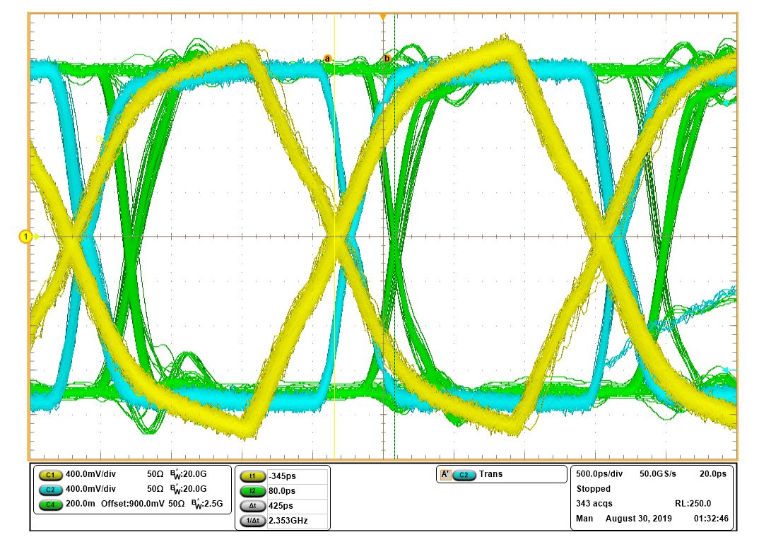
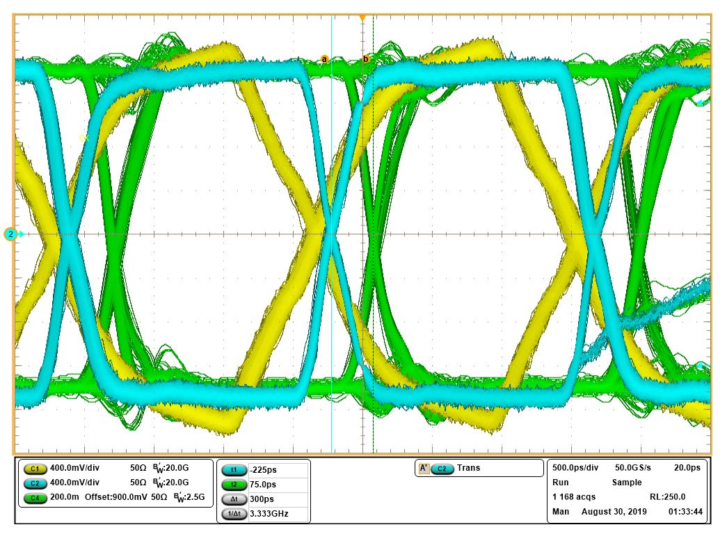
Where the signals are (all measured close to the CPU):

- C1 -> CK_p/n

- C2 -> DQS1_p/n

- C3 -> DQ8

2. Second measurement on read burst where timing fails:

- tDQSQ-Diff, DQ, DQS which is required to be less than +300ps. Measurement results show +396.45ps (with an average of 288.93ps and a low of -387.77ps).

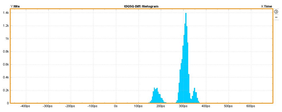
Signals are same as the previous measurement.

3. The third measurement is an signal integrity measurement where we do not meet the JEDEC:

- Vox(ac)DQS, DQS, DQS# where the low limit is 775mV and high limit 1.025V. From the measurement result we see the low limit is not met and results in 421.89mV.

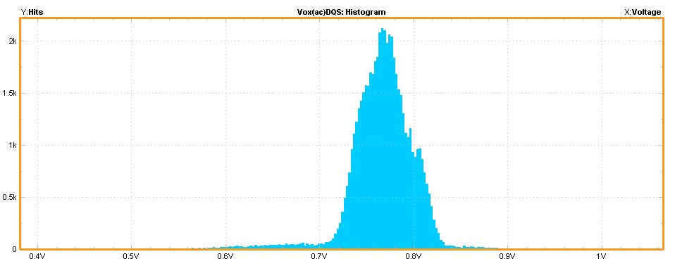
As shown in the histogram we do not meet this JEDEC spec.

Can you advice on these measurements and fails?

The design consist of a DDR2 (ISSI) device (IS43DR16640C-25DBLI) connected to the CPU (AM3351).

The DDR2 settings in the Sitara CPU are as follow:

arch/arm/include/asm/arch-am33xx/ddr_defs.h:28:#define IS43DR16640C25DBLI_EMIF_READ_LATENCY   0x100306
arch/arm/include/asm/arch-am33xx/ddr_defs.h:29:#define IS43DR16640C25DBLI_EMIF_SDCFG                   0x43845732
arch/arm/include/asm/arch-am33xx/ddr_defs.h:30:#define IS43DR16640C25DBLI_EMIF_SDREF                   0x2000040d
arch/arm/include/asm/arch-am33xx/ddr_defs.h:31:#define IS43DR16640C25DBLI_EMIF_TIM1                       0x0666a392
arch/arm/include/asm/arch-am33xx/ddr_defs.h:32:#define IS43DR16640C25DBLI_EMIF_TIM2                       0x142431ca
arch/arm/include/asm/arch-am33xx/ddr_defs.h:33:#define IS43DR16640C25DBLI_EMIF_TIM3                       0x0000021f
arch/arm/include/asm/arch-am33xx/ddr_defs.h:34:#define IS43DR16640C25DBLI_INVERT_CLKOUT            0x0
arch/arm/include/asm/arch-am33xx/ddr_defs.h:35:#define IS43DR16640C25DBLI_IOCTRL_VALUE               0x373
arch/arm/include/asm/arch-am33xx/ddr_defs.h:36:#define IS43DR16640C25DBLI_PHY_FIFO_WE                0x5d
arch/arm/include/asm/arch-am33xx/ddr_defs.h:37:#define IS43DR16640C25DBLI_PHY_WR_DATA               0x40
arch/arm/include/asm/arch-am33xx/ddr_defs.h:38:#define IS43DR16640C25DBLI_RATIO                              0x80
arch/arm/include/asm/arch-am33xx/ddr_defs.h:39:#define IS43DR16640C25DBLI_RD_DQS                          0x40
arch/arm/include/asm/arch-am33xx/ddr_defs.h:40:#define IS43DR16640C25DBLI_WR_DQS                         0x6

PCB trace lengths between CPU (U2000) and DDR2 (U4001) are as follow:

Net Length Time
DDR2_ADD0 30.654
U2000.F3:U4001.M8 30.654 0.18765
DDR2_ADD1 29.890
U2000.J2:U4001.M3 29.889 0.18297
DDR2_ADD2 30.391
U2000.D1:U4001.M7 30.391 0.18604
DDR2_ADD3 29.966
U2000.B3:U4001.N2 29.966 0.18344
DDR2_ADD4 30.377
U2000.E5:U4001.N8 30.377 0.18596
DDR2_ADD5 30.258
U2000.A2:U4001.N3 30.258 0.18523
DDR2_ADD6 30.559
U2000.B1:U4001.N7 30.559 0.18707
DDR2_ADD7 30.033
U2000.D2:U4001.P2 30.032 0.18385
DDR2_ADD8 30.570
U2000.C3:U4001.P8 30.570 0.18714
DDR2_ADD9 30.016
U2000.B2:U4001.P3 30.016 0.18375
DDR2_ADD10 30.270
U2000.E2:U4001.M2 30.270 0.1853
DDR2_ADD11 29.976
U2000.G4:U4001.P7 29.976 0.1835
DDR2_ADD12 29.727
U2000.F4:U4001.R2 29.727 0.18198
DDR2_ADD13 30.044
U2000.H1:U4001.R8 30.044 0.18392
DDR2_BA0 29.997
U2000.A3:U4001.L2 29.997 0.18363
DDR2_BA1 30.262
U2000.E1:U4001.L3 30.262 0.18525
DDR2_BA2 30.175
U2000.B4:U4001.L1 30.175 0.18472
DDR2_CAS_N 30.260
U2000.F1:U4001.L7 30.260 0.18524
DDR2_CKE 30.046
U2000.G3:U4001.K2 30.046 0.18394
DDR2_CK_N 29.028
U2000.C1:U4001.K8 29.029 0.1774
DDR2_CK_P 30.298
U2000.C2:U4001.J8 30.298 0.18515
DDR2_CS0_N 30.306
U2000.H2:U4001.L8 30.306 0.18552
DDR2_ODT 29.862
U2000.G1:U4001.K9 29.862 0.18281
DDR2_RAS_N 30.384
U2000.F2:U4001.K7 30.384 0.186
DDR2_WE_N 30.282
U2000.A4:U4001.K3 30.283 0.18538
DDR2_BYTE0(11)
DDR2_DAT0 17.647
U2000.N4:U4001.C8 17.647 0.10803
DDR2_DAT1 16.709
U2000.P4:U4001.C2 16.709 0.10229
DDR2_DAT2 16.851
U2000.P2:U4001.D7 16.851 0.10316
DDR2_DAT3 17.329
U2000.P1:U4001.D3 17.329 0.10608
DDR2_DAT4 16.085
U4001.D1:U2000.P3 16.085 0.09847
DDR2_DAT5 17.386
U2000.T1:U4001.D9 17.386 0.10643
DDR2_DAT6 15.816
U2000.T2:U4001.B1 15.816 0.09682
DDR2_DAT7 18.325
U2000.R3:U4001.B9 18.325 0.11218
DDR2_DQM0 16.827
U2000.N3:U4001.B3 16.827 0.10301
DDR2_DQS0_N 15.926
U2000.R2:U4001.A8 15.926 0.09733
DDR2_DQS0_P 15.876
U2000.R1:U4001.B7 15.876 0.09703
DDR2_BYTE1(11)
DDR2_DAT8 16.606
U2000.K2:U4001.G8 16.606 0.10166
DDR2_DAT9 15.269
U2000.K1:U4001.G2 15.269 0.09347
DDR2_DAT10 16.170
U2000.M3:U4001.H7 16.170 0.09899
DDR2_DAT11 15.871
U2000.M4:U4001.H3 15.871 0.09716
DDR2_DAT12 14.279
U2000.M2:U4001.H1 14.279 0.08741
DDR2_DAT13 16.648
U2000.M1:U4001.H9 16.648 0.10192
DDR2_DAT14 14.158
U2000.N2:U4001.F1 14.158 0.08667
DDR2_DAT15 16.420
U2000.N1:U4001.F9 16.420 0.10052
DDR2_DQM1 16.364
U2000.K3:U4001.F3 16.364 0.10017
DDR2_DQS1_N 15.674
U2000.L2:U4001.E8 15.674 0.0958
DDR2_DQS1_P 15.727
U2000.L1:U4001.F7 15.727 0.09612

Thank you in advance!

Francois.

  • Francois, be sure to double check the layout guidelines in the datasheet for DDR2.  I see a big violation on the differential clock and some which are close, which may be contributing to your compliance issues:

    1.  Datasheet:  CK differential pair skew length mismatch 25 mils (0.635mm)

    Board:  CK_P - CK_N length = 30.298 - 29.028 = 1.27mm

    2. Datasheet:DQ[x]-to-DQS[x] skew length mismatch 100 mils (2.54mm)

    Board: DAT7 - DQS0_N = 18.325 - 15.876 = 2.45mm (not technically a violation, but very close to the limit compared to the other data signals) 

    3. DQ[x]-to-DQ[x] skew length mismatch 100 mils (2.54mm)

    Board: DAT13 - DAT14 = 16.648 - 14.158 = 2.49mm (not technically a violation, but close) 

    Board: DAT7 - DAT6 = 18.325 - 15.816 = 2.509 (not technically a violation, but very close)


    I just mention the ones that are close because there may be other specifications (eg, center to center spacing or other skew mismatches) which may also be in violation which may be affecting your results.

    Regards,

    James 

  • Hi James,

    Thank you for pointing this out, we are updating the design as we speak. I'll let you know if this solves the problems when we have the new boards.

    During qualification I also needed to tune the clock to comply to JEDEC. To comply I added a 100R parallel termination between p and n and 10R series termination in p and n signal. From measurements this is now pass but it is nowhere mentioned in the datasheet or in reference designs this termination I added should be added. Can you comment on this?

    We did found that our implementation on the differential DQS and CK is 90um trace width and 210um airgap to get the 100R differentials. After reviewing the datasheet we are now thinking of updating it to 100-100-100 um differentials. In this case we do also comply to the datasheet 2w spacing and impedance. Can you comment on this as well?

    Thank you in advance!

    Regards,

    Francois

  • Francois, 

    all of the read timing are signals generated by the DDR memory, not the AM335x.  Most likely timing distortion  would result from PCB layout and termination impedance issues.  JEDEC signal levels and requirements are defined at the pins of the DDR memory.  Taking these measurements close to the CPU will give you misleading results.  You should take these measurement at or near the DDR pins.

    Also, be sure to follow all of the guidance on stackup, placement, trace widths, etc from the datasheet.  Things like split ground planes or routing not adjacent to ground planes can cause impedance mismatches which will distort your signal.  This may be the reason you need to add series and/or parallel termination. 

    Regards,

    James

  • James,

    Sorry I may be a bit unclear in my previous reply.

    The question of adding parallel and series termination was not about a measurement mentioned above (from my first post), but is an additional question.

    The differential signal where I added the termination is only to the CK_p/n, which I believe is an output only on the AM335x side. We are measuring this signal at the DDR2 device side. In the DDR2 device there is no on-die termination (as far as I could find) so the signal was to strong at the DDR2 device. With the termination added I was able to get the signal within JEDEC requirements. I was wondering about this because there is no termination inside the DDR2 Device, shouldn't this be stated in the datasheet of the Sitara?

    The other question about the implementation of the differential signals we have a problem with the requirements stated in the datasheet (I miss interpret my colleague who drawing the PCB).

    Our implementation is 90-210-90 um to get 100R impedance differential. We use 100um to get 50R impedance single ended. This violates the requirement of center-to-center (2w) of the datasheet.

    If we do want to follow the datasheet we can implement the differentials like 100-100-100 um which satisfies the center-to-center requirement. With our stack-up we satisfy the impedance requirement for the single ended signal trace of 50R. But the impedance of the differential will be lower than 100R which violates the 2x Zo requirement stated in the datasheet. What is in your opinion the best way to implement the differentials?

    Regards,

    François

  • Hi Francois, if the CK signal was too strong, have you tried adjusting the drive strength for it from the AM335x side?  What are your drive strength settings?  If you have JTAG access, run the script below and send back the resulting file:

    git.ti.com/.../am335x-ddr-analysis.dss 

    Instructions for running the file can be found here:  http://git.ti.com/sitara-dss-files/am335x-dss-files/blobs/master/README

    As for your differential impedance, how is CK and CKn routed?  Ideally, they should be routed on an outer layer with no layer transitions.  This will allow you to control the impedance mismatches much easier.  I believe you can move slightly wider that 2w to achieve the 2x Zo if needed.

    Regards,

    James  

  • Hi James,

    I have run the script on a board and the following output it printed: 

    Switched to DAP_DebugSS
    Read value of 2b94402e from Device_ID register.
    CONTROL: device_id = 0x2b94402e
      * AM335x family
      * Silicon Revision 2.1
    
    CONTROL: control_status = 0x008c0356
      * SYSBOOT[15:14] = 10b (25 MHz)
    CM_CLKSEL_DPLL_DDR = 0x00010a18
      * DPLL_MULT = 266 (x266)
      * DPLL_DIV = 24 (/25)
    CM_DIV_M2_DPLL_DDR = 0x00000201
      * CLKST = 1: M2 output clock enabled
      * DIVHS = 1 (/1)
    
    DPLL_DDR Summary
     -> F_input = 25 MHz
     -> CLKOUT_M2 = DDR_PLL_CLKOUT = 266 MHz
    
    EMIF: SDRAM_CONFIG = 0x43845732
      * Bits 31:29 (reg_sdram_type) set for DDR2
      * Bits 28:27 (reg_ibank_pos) set to 0
      * Bits 26:24 (reg_ddr_term) set for 50 Ohm (011b)
      * Bit  23    (reg_ddr2_ddqs) set to differential DQS.
      * Bits 19:18 (reg_sdram_drive) set for weak drive (01b)
      * Bits 15:14 (reg_narrow_mode) set to 1 -> 16-bit EMIF interface
      * Bits 13:10 (reg_cl) set to 5 -> CL = 5
      * Bits 09:07 (reg_rowsize) set to 6 -> 15 row bits
      * Bits 06:04 (reg_ibank) set to 3 -> 8 banks
      * Bits 02:00 (reg_pagesize) set to 2 -> 10 column bits
    
    EMIF: PWR_MGMT_CTRL = 0x00000000
     * Bits 10:8 reg_lp_mode set to 0, auto power management disabled
     * Warning: Bits 7:4 (reg_sr_tim) are in violation of Maximum Self-Refresh Command Limit
       -> Please see the silicon errata (DDR3: JEDEC Compliance for Maximum Self-Refresh Command Limit) for more details.
       -> This is only an issue if used in conjunction with reg_lp_mode=2.
    
    DDR PHY: DDR_PHY_CTRL_1 = 0x00100306
      * Bits 9:8 (reg_phy_rd_local_odt) to 3 -> half thevenin termination
      * Bits 4:0 (reg_read_latency) set to 6
        -> If PHY_INVERT_CLKOUT=0, this is an appropriate value.
        -> If PHY_INVERT_CLKOUT=1, this is too small.
        -> PHY_INVERT_CLKOUT is a write-only register, so this needs to be
        -> inspected closely in the code and RatioSeed spreadsheet.
    
    *********************
    *** Register Dump ***
    *********************
    
    *(0x4c000000) = 0x40443403
    *(0x4c000004) = 0x40000004
    *(0x4c000008) = 0x43845732
    *(0x4c00000c) = 0x00000000
    *(0x4c000010) = 0x2000040d
    *(0x4c000014) = 0x0000040d
    *(0x4c000018) = 0x0666a392
    *(0x4c00001c) = 0x0666a392
    *(0x4c000020) = 0x142431ca
    *(0x4c000024) = 0x142431ca
    *(0x4c000028) = 0x0000021f
    *(0x4c00002c) = 0x0000021f
    *(0x4c000038) = 0x00000000
    *(0x4c00003c) = 0x00000000
    *(0x4c000054) = 0x00ffffff
    *(0x4c000058) = 0x8000140a
    *(0x4c00005c) = 0x00021616
    *(0x4c000080) = 0x003f9180
    *(0x4c000084) = 0x00026ee7
    *(0x4c000088) = 0x00010000
    *(0x4c00008c) = 0x00000000
    *(0x4c000090) = 0x89526de3
    *(0x4c000098) = 0x00050000
    *(0x4c00009c) = 0x00050000
    *(0x4c0000a4) = 0x00000000
    *(0x4c0000ac) = 0x00000000
    *(0x4c0000b4) = 0x00000000
    *(0x4c0000bc) = 0x00000000
    *(0x4c0000c8) = 0x00000000
    *(0x4c0000d4) = 0x00000000
    *(0x4c0000d8) = 0x00000000
    *(0x4c0000dc) = 0x00000000
    *(0x4c0000e4) = 0x00100306
    *(0x4c0000e8) = 0x00100306
    *(0x4c000100) = 0x00000000
    *(0x4c000104) = 0x00000000
    *(0x4c000108) = 0x00000000
    *(0x4c000120) = 0x00000305
    
    ************************
    *** IOCTRL Registers ***
    ************************
    
    CONTROL: DDR_CMD0_IOCTRL = 0x00000373
      * ddr_ba2 Pullup/Pulldown disabled
      * ddr_wen Pullup/Pulldown disabled
      * ddr_ba0 Pullup/Pulldown disabled
      * ddr_a5 Pullup/Pulldown disabled
      * ddr_ck Pullup/Pulldown disabled
      * ddr_ckn Pullup/Pulldown disabled
      * ddr_a3 Pullup/Pulldown disabled
      * ddr_a4 Pullup/Pulldown disabled
      * ddr_a8 Pullup/Pulldown disabled
      * ddr_a9 Pullup/Pulldown disabled
      * ddr_a6 Pullup/Pulldown disabled
      * Bits 9:5 control ddr_ck and ddr_ckn
        - Slew slowest
        - Drive Strength 8 mA
      * Bits 4:0 control ddr_ba0, ddr_ba2, ddr_wen, ddr_a[9:8], ddr_a[6:3]
        - Slew fast
        - Drive Strength 8 mA
    CONTROL: DDR_CMD1_IOCTRL = 0x00000373
      * ddr_a15 Pullup/Pulldown disabled
      * ddr_a2 Pullup/Pulldown disabled
      * ddr_a12 Pullup/Pulldown disabled
      * ddr_a7 Pullup/Pulldown disabled
      * ddr_ba1 Pullup/Pulldown disabled
      * ddr_a10 Pullup/Pulldown disabled
      * ddr_a0 Pullup/Pulldown disabled
      * ddr_a11 Pullup/Pulldown disabled
      * ddr_casn Pullup/Pulldown disabled
      * ddr_rasn Pullup/Pulldown disabled
      * Bits 4:0 control ddr_15, ddr_a[12:10], ddr_a7, ddr_a2, ddr_a0, ddr_ba1, ddr_casn, ddr_rasn
        - Slew fast
        - Drive Strength 8 mA
    CONTROL: DDR_CMD2_IOCTRL = 0x00000373
      * ddr_cke Pullup/Pulldown disabled
      * ddr_resetn Pullup/Pulldown disabled
      * ddr_odt Pullup/Pulldown disabled
      * ddr_a14 Pullup/Pulldown disabled
      * ddr_a13 Pullup/Pulldown disabled
      * ddr_csn0 Pullup/Pulldown disabled
      * ddr_a1 Pullup/Pulldown disabled
      * Bits 4:0 control ddr_cke, ddr_resetn, ddr_odt, ddr_csn0, ddr_[a14:13], ddr_a1
        - Slew fast
        - Drive Strength 8 mA
    CONTROL: DDR_DATA0_IOCTRL = 0x00000373
      * ddr_d8 Pullup/Pulldown disabled
      * ddr_d9 Pullup/Pulldown disabled
      * ddr_d10 Pullup/Pulldown disabled
      * ddr_d11 Pullup/Pulldown disabled
      * ddr_d12 Pullup/Pulldown disabled
      * ddr_d13 Pullup/Pulldown disabled
      * ddr_d14 Pullup/Pulldown disabled
      * ddr_d15 Pullup/Pulldown disabled
      * ddr_dqm1 Pullup/Pulldown disabled
      * ddr_dqs1 and ddr_dqsn1 Pullup/Pulldown disabled
      * Bits 9:5 control ddr_dqs1, ddr_dqsn1
        - Slew slowest
        - Drive Strength 8 mA
      * Bits 4:0 control ddr_d[15:8], ddr_dqm1
        - Slew fast
        - Drive Strength 8 mA
    CONTROL: DDR_DATA1_IOCTRL = 0x00000373
      * ddr_d0 Pullup/Pulldown disabled
      * ddr_d1 Pullup/Pulldown disabled
      * ddr_d2 Pullup/Pulldown disabled
      * ddr_d3 Pullup/Pulldown disabled
      * ddr_d4 Pullup/Pulldown disabled
      * ddr_d5 Pullup/Pulldown disabled
      * ddr_d6 Pullup/Pulldown disabled
      * ddr_d7 Pullup/Pulldown disabled
      * ddr_dqm0 Pullup/Pulldown disabled
      * ddr_dqs0 and ddr_dqsn0 Pullup/Pulldown disabled
      * Bits 9:5 control ddr_dqs0, ddr_dqsn0
        - Slew slowest
        - Drive Strength 8 mA
      * Bits 4:0 control ddr_d[7:0], dqm0
        - Slew fast
        - Drive Strength 8 mA
    CONTROL: DDR_IO_CTRL = 0x00000000
      * Bit 31: DDR_RESETn controlled by EMIF.
      * Bit 28 (mddr_sel) configured for SSTL, i.e. DDR2/DDR3/DDR3L operation.
    CONTROL: VTP_CTRL = 0x00010167
      * VTP not disabled (expected in normal operation, but not DS0).
    CONTROL: VREF_CTRL = 0x00000000
      * VREF supplied externally (typical).
    CONTROL: DDR_CKE_CTRL = 0x00000001
      * CKE controlled by EMIF (normal/ungated operation).
    

    From this output I see that our clock settings are:

    - Slew slowest
    - Drive Strength 8 mA

    So do you recommend to reduce the drive strength of the clock signal? (The same settings are used for DQSx, this signal is near the 1V - VSWING(max) parameter, only here the ODT is present where it is not for the clock.). Without my added parallel and series termination on the clock differential the VSWING(max) is almost 1.8V.

    Additionally for your information we have updated the board on the violations pointed out and re-checked the board. Within a few weeks I will have updated boards to test.

    Thank you.

    Regards,

    François

  • Francois, yes you can try to reduce the clock drive strength and see the effects.  Also, i noticed you are mixing and matching slew rates for the signals.  I think i would at least match up the addr/clk slew rates, and then the data/DQS/DM slew rates.  

    REgards,

    James

  • Hi James,

    We received the boards and have updated the settings so we are at the point of remeasuring the DDR2.

    One thing we noticed when I used the am335x-ddr-analysis.dss to read the settings through JTAG is that we see different settings between u-boot and Linux. When we booted to u-boot the settings we set are correct, but when the boot continues and loads Linux it sets the DDR2 settings to different settings.

    I'm not a software engineer so I hope it is not a trivial question but does Linux uses its own DDR2 settings? Or do I overlook something here with the JTAG script, where the registers are blocked from reading? I do get a lot of 0x00 from the registers back but the system does work.

    Thank you for the support!

    Regards,

    François

  • Francois Veger said:
    One thing we noticed when I used the am335x-ddr-analysis.dss to read the settings through JTAG is that we see different settings between u-boot and Linux. When we booted to u-boot the settings we set are correct, but when the boot continues and loads Linux it sets the DDR2 settings to different settings.

    That's unexpected.  Can you please zip up the output of the script as observed during u-boot and Linux?  I'd like to better understand precisely what is changing, e.g. is it a few isolated registers or does it appear to be fully reconfigured?

  • JTAG_read.zip

    In the added zip 2 logs are present. First I read the settings through JTAG when I halted boot at the U-boot stage. Second read was after entire boot sequence.

    I checked the reads but when Linux is booted I appears that JTAG is not able to read the settings anymore. Maybe Linux blocks JTAG reads? 

  • Execute this command from the Linux console before running the script:

    devmem2 0x44e00414 w 0x12500002