This thread has been locked.

If you have a related question, please click the "Ask a related question" button in the top right corner. The newly created question will be automatically linked to this question.

Compiler/TDA4VM: How to enable PCIE internal clock on dts

Part Number: TDA4VM

Tool/software: TI C/C++ Compiler

Hi TI members:

For project request, we are studying how to enable PCIE internal clock output function.

There is some code about pcie0 in k3-j721e-main.dtsi

 974         pcie0: pcie@2900000 {
 975                 compatible = "ti,j721e-pcie";
 976                 reg = <0x00 0x02900000 0x00 0x1000>,
 977                       <0x00 0x02907000 0x00 0x400>,
 978                       <0x0 0x02905000 0x0 0x00000400>;
 979                 reg-names = "intd_cfg", "user_cfg", "vmap";
 980                 #address-cells = <2>;
 981                 #size-cells = <2>;
 982                 ranges;
 983                 ti,syscon-pcie-ctrl = <&pcie0_ctrl>;
 984                 max-link-speed = <3>;
 985                 num-lanes = <2>;
 986                 power-domains = <&k3_pds 239 TI_SCI_PD_EXCLUSIVE>;
 987                 clocks = <&k3_clks 239 1>;
 988                 clock-names = "fck";

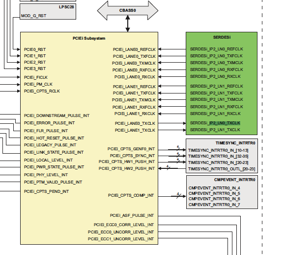
I am not sure is this  "clocks = <&k3_clks 239 1>;" just mean below clock pin 

So I have a few questions,

Q1: Is my understand about the clocks k3_clks right? 

Q2: is there any document to explain what means of the number parameters(239 1) in clocks?

Q3: how to set PCIE_REFCLK1 is output?

if my description is not clean,

please let me know,

Thanks a lot!!!

BR

Sentinen Chen

  • Sentinen, 

    The DTS entry you mentioned is for PCIe0, but seems you trying to enable PCIe_REFCLK1 (on the 2Lane slot). So I use PCIe0 as example:

    "clocks = <&k3_clks 239 1>" refers to Device ID 239 (PCIe0), Clock ID 1 (DEV_PCIE0_PCIE_CBA_CLK). they are defined in the System Firmware user guide. 

    http://software-dl.ti.com/tisci/esd/19_12_01/5_soc_doc/j721e/clocks.html

    I checked J721E EVM schematics, it seems using external REFCLK for SERDES1 with an external clockgen device, though the x2 slot defaults to RC function. But SERDES2 on PCIe2 are configured for SOC to provide a common refclk to the SSD card. You can refer to the "serdes_wiz2" section in the same DTSI file. Note kernel configure to enable PCIe RC are at:

    http://software-dl.ti.com/jacinto7/esd/processor-sdk-linux-jacinto7/latest/exports/docs/linux/Foundational_Components/Kernel/Kernel_Drivers/PCIe/PCIe_Root_Complex.html

    let me know if you have further questions. 
    jian

  • Hi Jian:

    Thanks for your reply.


    1. but seems you trying to enable PCIe_REFCLK1 (on the 2Lane slot).

    ==> Yes, it's my mistake. we want to enable PCIE_REFCLK0 as internal clock currently. 

    2. But SERDES2 on PCIe2 are configured for SOC to provide a common refclk to the SSD card

    ==> I check the schemtics. Does your's SSD card mean PCIE_M2_interface in schemtics PROC079E3B(001)_SCH.pdf page 54? 

    If yes, It seem the PCIE_M2_interface is also use external clk.

    Can you help to check again?

    BR

    Sentinen Chen

  • Sentinen:

    Yes on Page 54 of the same document you mentioned, you would use the "SOC" option under "CLOCK ROOT SELECTION", where you install C1, C2, R3, R4, and remove R1, R2, R5, R6. 

    You can use similar resistor configuration on the "x4LANE PCIe Interface" on Page 53 for PCIe1.

    Then you need to configure "serdes_wiz1" in the DTSI to use internal refclk. I can look up if not clear from: 

    http://software-dl.ti.com/tisci/esd/19_12_01/5_soc_doc/j721e/clocks.html

    Jian

  • Hi Jian:

    OK,it is about HW rework.

    But back to dts, I compare "serdes_wiz0" and "serdes_wiz2".

    because they all use external clock. I can't refer it.

    1. In clock domain, there are many output clock can choose (clock ID 16~43).

    which one suggest to use?

    2. Do you have related patch about serdes_wizX which use internal clock can provide to us? 

    BR

    Sentinen Chen 

  • Hi Jian:

    I just try to follow below picture on TRM to output PCIE internal clock,

    let PCIEi clock set PCIEi_LANE0_TXCLK and SERDES clock set SERDESi_IP2_LN0_TXCLK

    below is my modify on dts

    --- a/arch/arm64/boot/dts/ti/k3-j721e-main.dtsi
    +++ b/arch/arm64/boot/dts/ti/k3-j721e-main.dtsi
    @@ -633,7 +633,7 @@
                    #address-cells = <2>;
                    #size-cells = <2>;
                    power-domains = <&k3_pds 292 TI_SCI_PD_EXCLUSIVE>;
    -               clocks = <&k3_clks 292 5>, <&k3_clks 292 11>, <&dummy_cmn_refclk>;
    +               clocks = <&k3_clks 292 9>, <&k3_clks 292 11>, <&dummy_cmn_refclk>;
                    clock-names = "fck", "core_ref_clk", "ext_ref_clk";
                    assigned-clocks = <&k3_clks 292 11>, <&k3_clks 292 0>;
                    assigned-clock-parents = <&k3_clks 292 15>, <&k3_clks 292 4>;
    @@ -984,7 +984,7 @@
                    max-link-speed = <3>;
                    num-lanes = <2>;
                    power-domains = <&k3_pds 239 TI_SCI_PD_EXCLUSIVE>;
    -               clocks = <&k3_clks 239 1>;
    +               clocks = <&k3_clks 239 30>;
                    clock-names = "fck";
    
                    pcie0_rc: pcie@d000000 {

    But after I try my new dtb file, the clock form SOC still can not output. 

    I also try to modify core_ref_clk setting, but it always make another problem let my wiz@5000000 register failed.

    I am not sure my idea is correct or not.

    Can you give us more detail suggestions about enable pcie internal clock?

    BR

    Sentinen Chen 

  • Sentinen, 

    There are several steps involved here:

    1. Set DEV_SERDES_16G1_CORE_REF_CLK_PARENT_HSDIV4_16FFT_MAIN_2_HSDIVOUT4_CLK as the input to the core_refclk/1;

    2. Set SERDES1 to use core_refclk (on-chip clock)

    3. Enable DEV_SERDES_16G1_REF1_OUT_CLK on SERDES1, this clock goes to the ACSPCIe mux;

    4. Set ACSPCIe mux 

    It seems TRM does not have enough information. I will try to get a sample DTS for you to try. 

    Sorry for the delay

    Jian

  • Hi Jian:

    I try to follow your steps on SERDES0 & PCIE0

    1. Set DEV_SERDES_16G1_CORE_REF_CLK_PARENT_HSDIV4_16FFT_MAIN_2_HSDIVOUT4_CLK as the input to the core_refclk/1;

    2. Set SERDES0 to use core_refclk (on-chip clock)

    3. Enable DEV_SERDES_16G1_REF1_OUT_CLK on SERDES0, this clock goes to the ACSPCIe mux;

    4. Set ACSPCIe mux

    In step1~3, I think the DEV_SERDES_16G1_CORE_REF_CLK_PARENT_HSDIV4_16FFT_MAIN_2_HSDIVOUT4_CLK already be the assigned_clock-parents,

    so I only do below modify

    +++ b/arch/arm64/boot/dts/ti/k3-j721e-main.dtsi
    @@ -633,7 +633,7 @@
                    #address-cells = <2>;
                    #size-cells = <2>;
                    power-domains = <&k3_pds 292 TI_SCI_PD_EXCLUSIVE>;
    -               clocks = <&k3_clks 292 5>, <&k3_clks 292 11>, <&dummy_cmn_refclk>;
    +               clocks = <&k3_clks 292 34>, <&k3_clks 292 0>, <&dummy_cmn_refclk>;
                    clock-names = "fck", "core_ref_clk", "ext_ref_clk";
                    assigned-clocks = <&k3_clks 292 11>, <&k3_clks 292 0>;
                    assigned-clock-parents = <&k3_clks 292 15>, <&k3_clks 292 4>;
    @@ -662,7 +662,7 @@
                            clock-output-names = "wiz0_refclk_dig";
                            #clock-cells = <0>;
                            assigned-clocks = <&wiz0_refclk_dig>;
    -                       assigned-clock-parents = <&k3_clks 292 11>;
    +                       assigned-clock-parents = <&k3_clks 292 0>;
                    };

    and in step4, after sd-boot finished, I use JTAG & CCS tool to modify register CTRLMMR_PCIE_REFCLK0_CLKSEL,

    value as below

    I also read the CTRLMMR_SERDES0_CLKSEL register, it seem already to set as "3h - MAIN_PLL2_HSDIV4_CLKOUT"

    But after those modifies, Internal clock still can not output. 

    Did I lose any part to modify, or my understand has wrong?

    BR

    Sentinen Chen

  • Sentinen, 

    CTRLMMR_PCIE_REFCLK0_CLKSEL stetting looks right. 

    You may also need to enable the ACSPCIe pads, by :

        CTRLMMR_ACSPCIE0_CTRL: 0x0003->0x0000;  //This line enables the PCIE_REFCLK0_P/M output buffers, they were disabled by default.

    let me know how it goes. 

    Jian

  • Sentinen, 

    Beside of the CTRLMMR_ACSPCIE0_CTRL register mentioned above on Step 4. I also like  to confirm we configured SERDES corrected in Step #2, specifically, can you also check two registers within the SERDES block, they are:

    1. SERDES_RST register at address: 0x05000000 + 0x40C:  Bit 28 and Bit 29 shall be set to allow SERDES to use pma_cmn_refclk1_int  (core_refclk) 
    2. PHY_PMA_CMN_REGISTERS_PHY_PMA_CMN_CTRL at  address: 0x05000000 + 0xe000, Bit 7 shall be set. this bit enabled the  cmn_refclk1_rcv_out (refclk1_out), that connected to input of the ACSPCIe0 mux. 

    Please send me the full value of these two registers in your system, as we may try a few things. It seems SERDES chapter is not in the TRM ver1A yet. So you are a bit blind. 

    Jian

  • Hi Jian:

    After I modify CTRLMMR_ACSPCIE0_CTRL bit 0, 

    I can see clock pin only high to 1.8V, but it still not a clock signal.

    And I also check 0x05000040c & 0x0500e000 reigster, but there are a few questions:

    Q1. bit 28 on 0x05000040c seem a reserved bit.

    Q2:

    I try to use CCS tool to modify SERDES_16G0's register's bit, but register value can't change as my modify.

    no matter on 0x05000040c or 0x0500e000c, manual modify doesn't have effect.

    I also try to connect different core to test(CortexA72_0_1, MCU_Cortex_R5_0,... ), but it seem not work.

    Do you have any idea on this situation?

    BR

    Sentinen Chen

  • Sentinen, 

    Regarding to your Q's:

    Q1: The register is not the _SERDES_RST register. Instead you showed  CMN_CTRL_CDBREG_CMN_PWRISO_OVRD_PREG__CMN_PWRISO_CTRL_PREG at offset 0x40. Please advance to offset (0x40C) and confirm if you can see the register name _xxx_SERDES_RST. Where xxx can be either SERDES_16G0 or *WIZ* (not sure how the register names were coded in CCS). 

    Q2. Bit 27 of SERDES_RST is write-protected if Bit 31 of the same register is "1". So please try to fist set Bit 31 of the same register to "0", the see if you can access Bit 27. 

    PHY_PMA_CMN_REGISTERS_PHY_PMA_CMN_CTRL register - only Bit 15:14 and Bit 7:6 are RW, other bits are read-only. but there are no mentioning of any protection on this register. 

    I will check to see if possible to share these register definitions to you before they are published in the TRM. 

    Jian

  • Hi Jian:

    Sorry, it's my misunderstanding。

    Below is 0x0500040C & 0x0500e000 value after I modify. 

    0x0500040C:

    0x0500e000:

    but in this settings, internal clock still only high to 1.8v. 

    BR

    Sentinen Chen

  • Hi Jian,

    Is there any update for the PCIe internal clock enabling?

    We need a clear guideline to enable it.

    Is it possible for TI to provide a brief document for it?

    Thanks,

    Alex Lin

  • Sentinen, 

    Sorry about the delay. Both registers seems right on the RW bits. But in the PHY_PMA_CMN_CTRL register, it seems  Bit 12 and Bit 13 are still set - can you confirm SERDES already configured and PLLs are locked?

    I did confirm with our software team there are no SDK support for internal refclk currently, and in the process of getting some register definitions to you. I think the fastest approach may be to debug on your setup. 

    regards

    Jian

  • Hi Jian:

    Are there any update form your software team? 

    and 

    can you confirm SERDES already configured

    ==> What part of SERDES configured do you mean, dts?  or  register? 

    BR

    Sentinen Chen

  • Hi Jian:

    Sorry to brother you, 

    Can you share your software team's schedule about enable PCIE internal clock to us?

    I need to evaluate what time we can rework our EVM board HW part to external clock.

    our colleague still wait the EVM board to test. 

    BR

    Sentinen Chen

  • Sentinen, 

    Sorry for the delay. I have not received development plan to enable internal clocking. 

    In parallel,  I received confirmation to release a few relevant register definitions to you, so we can program the clock via barematel. Please let me know if you need the full driver support. Since REFCLK must satisfy PCIe specification on timing sequence in reference to PERST# signal, you may need to control both signals to get the card to work properly. 

    In my earlier question to you - if you already have all (PHY registers -> clock mux -> IO enable) the muxes set, then the last thing to check is SERDES PLL is locked. I will send you these register bits in 1-2 days.

    Jian

  • Hi Jian:

    so we can program the clock via barematel. Please let me know if you need the full driver support

    ==> Yes, we need to set all register in dts & driver in finally, if you can provide us full driver support is better. But the first priority thing is enable internal clock successfully.

    the last thing to check is SERDES PLL is locked. I will send you these register bits in 1-2 days.

    ==> Is there any update information about register bits? 

    BR

    Sentinen Chen