This thread has been locked.

If you have a related question, please click the "Ask a related question" button in the top right corner. The newly created question will be automatically linked to this question.

TDA2EX17EVM: TDA2 EMIF setting for TIDL

Part Number: TDA2EX17EVM

Hi Champs:

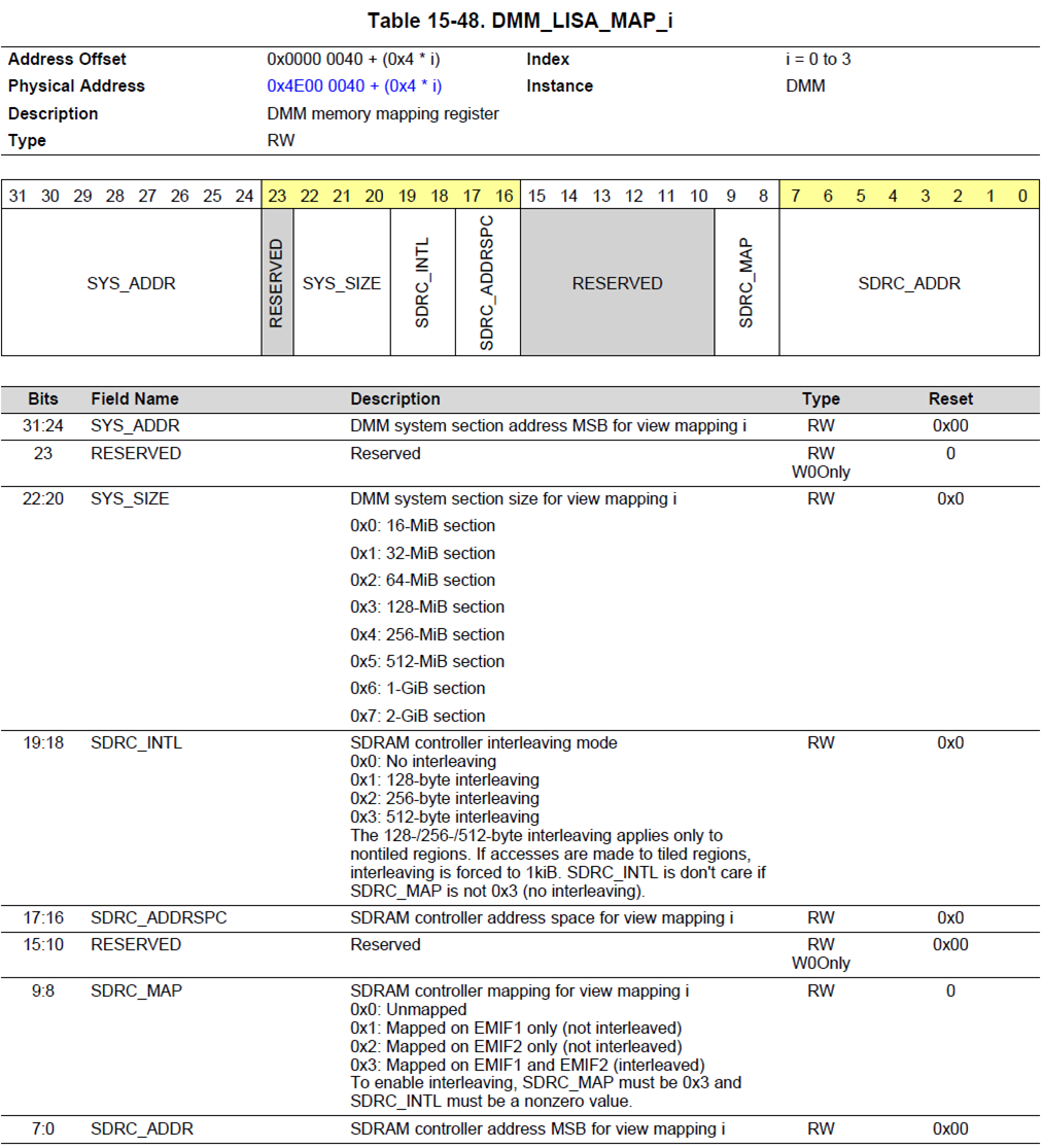
Customer is making the TIDL SSD for 720P, he is able to change the EMIF from 512MB to 512X2MB (Dual EMIF) as expected.

Now, he is asking if we are able to enlarge the SR1 ?

and can he modify with DUAL_EMIF with 1GB_512MB?

Please comment, thanks.

BR Rio

  • Hi,

    Can you comment on what "SR1" refers to?

    Also, what is meant by "1GB_512MB"? How does it differ than "512x2MB"?

    Best regards,
    Kevin

  • Hi,

    This is wxchen, the Rio's customer.

    1) I wanna know how to enlarge heap size on RTOS(SR1_FRAME_BUFFER_SIZE in mem_segment_definition_bios.xs, please correct  me if i wrong) at EMIFMODE=DUAL_EMIF_2X512MB setup.

        is it possible to having continuous memory on RTOS using both of EMIF1 & EMIF2?

    2) I also wanna know how to setup EMIDMODE=DUAL_EMIF_1GB_512MB and SINGLE_EMIF_1GB,

        I have referred the settings written on https://e2e.ti.com/support/processors/f/791/p/613857/2277707, but evm-board will stuck on booting.

        Is there any document indicating that changing memory map to DUAL_EMIF_1GB_512MB and SINGLE_EMIF_1GB? ( i found how to change memory map to DUAL_EMIF_2X512MB on VisionSDK_UserGuide_MemoryMap.pdf in VSDK, and i successed changing memory map to DUAL_EMIF_2X512MB by steps of that document. )

    3) In addition, what’s exactly HW setup for EMIFMODE=DUAL_EMIF_2X512MB? Is it using two EMIF modules and dual 512 MB DDR chips for each EMIF?

    Thanks

    Best regards,
    Wxchen

  • HI,

    The  supported EMIFMODE option in TDA2XX are 

    EMIFMODE = SINGLE_EMIF_512MB (default) or you can set below options
    DUAL_EMIF_1GB_512MB or
    DUAL_EMIF_2X512MB or
    SINGLE_EMIF_256MB

    NOTE:
    DUAL_EMIF_1GB_512MB : uses EMIF2 - 1GB and EMIF1 512MB, BUT in non-interleaved mode
    Vision SDK uses only 1GB hence effectivly this is single EMIF
    non-interleaved mode for Vision SDK
    0x8000_0000 - 0xBFFF_FFFF is mapped to EMIF2
    0xC000_0000 - 0xDFFF_FFFF is mapped to EMIF1
    DUAL_EMIF_2X512MB : uses EMIF1 and EMIF 512MB each in interleaved mode
    0x8000_0000 - 0x9FFF_FFFF is interleaved between EMIF1 and EMIF2
    SINGLE_EMIF_256MB : uses EMIF1 with 256MB
    0x8000_0000 - 0x8FFF_FFFF is mapped to EMIF1
    SINGLE_EMIF_512MB : uses EMIF1 with 512MB
    0x8000_0000 - 0x9FFF_FFFF is mapped to EMIF1

    By default, TDA2XX is configured with SINGLE_EMIF_512MB & here we will get SR1 memory around 250MB. If it is not sufficient for TIDL processing you choose the DUAL_EMIF_2X512MB option. In this configuration, we will get SR1 around 430MB. After choosing EMIFMODE=DUAL_EMIF_2X512MB we have to apply some patches to work & this is already explained in the "VisionSDK_UserGuide_MemoryMap.pdf". But this is not updated with the latest SDK version. So please add the below changes in your code to work properly.

    diff --git a/apps/build/tda2xx/mem_segment_definition_bios.xs b/apps/build/tda2xx/mem_segment_definition_bios.xs
    index 9dda0630f..d21c0116f 100755
    --- a/apps/build/tda2xx/mem_segment_definition_bios.xs
    +++ b/apps/build/tda2xx/mem_segment_definition_bios.xs
    @@ -18,7 +18,7 @@ function getMemSegmentDefinition_external(core)
    MB=KB*KB;

    DDR3_ADDR = 0x80000000;
    - DDR3_SIZE = 512*MB;
    + DDR3_SIZE = 1024*MB;

    /*
    * In case of ECC_FFI_INCLUDE, DDR3_BASE_ADDR_1 and DDR3_BASE_SIZE_1
    @@ -27,7 +27,7 @@ function getMemSegmentDefinition_external(core)
    * If this DDR3_BASE_SIZE_0 is changed, update Ipu1_0.cfg
    */
    DDR3_BASE_ADDR_0 = DDR3_ADDR;
    - DDR3_BASE_SIZE_0 = 507*MB;
    + DDR3_BASE_SIZE_0 = 512*MB;

    /* The start address of the second mem section should be 16MB aligned.
    * This alignment is a must as a single 16MB mapping is used for EVE
    @@ -42,7 +42,7 @@ function getMemSegmentDefinition_external(core)
    * in non-cached virtual address of
    * DDR3_BASE_ADDR_1 + 512*MB
    */
    - DDR3_BASE_ADDR_1 = DDR3_BASE_ADDR_1+512*MB;
    + /* DDR3_BASE_ADDR_1= DDR3_BASE_ADDR_1+512*MB; */
    }

    DSP1_L2_SRAM_ADDR = 0x40800000;
    @@ -122,7 +122,7 @@ function getMemSegmentDefinition_external(core)
    if(java.lang.System.getenv("ECC_FFI_INCLUDE")=="yes")
    {
    /* Ensure ECC regions are 64kB aligned */
    - SR1_FRAME_BUFFER_SIZE = 297.5*MB;
    + SR1_FRAME_BUFFER_SIZE = 390*MB;
    SR1_BUFF_ECC_ASIL_SIZE = 1*MB;
    SR1_BUFF_ECC_QM_SIZE = 40*MB;
    SR1_BUFF_NON_ECC_ASIL_SIZE = 1*MB;
    @@ -132,7 +132,7 @@ function getMemSegmentDefinition_external(core)
    SR1_BUFF_ECC_ASIL_SIZE = 4*KB;
    SR1_BUFF_ECC_QM_SIZE = 4*KB;
    SR1_BUFF_NON_ECC_ASIL_SIZE = 4*KB;
    - SR1_FRAME_BUFFER_SIZE = 339.5*MB - (SR1_BUFF_ECC_ASIL_SIZE + SR1_BUFF_ECC_QM_SIZE + SR1_BUFF_NON_ECC_ASIL_SIZE);
    + SR1_FRAME_BUFFER_SIZE = 432*MB - (SR1_BUFF_ECC_ASIL_SIZE + SR1_BUFF_ECC_QM_SIZE + SR1_BUFF_NON_ECC_ASIL_SIZE);
    if(java.lang.System.getenv("OPENCL_INCLUDE") == "yes")
    {
    SR1_FRAME_BUFFER_SIZE = SR1_FRAME_BUFFER_SIZE - A15_0_DATA_SIZE_INC;
    @@ -189,7 +189,7 @@ function getMemSegmentDefinition_external(core)
    * be kept constant across all platforms and should match the increment
    * to heapStats.heapSize in utils_xmc_mpu.c
    */
    - EVE1_VECS_ADDR = DDR3_BASE_ADDR_0;
    + EVE1_VECS_ADDR = DDR3_BASE_ADDR_1 + 16*MB;
    EVE1_CODE_ADDR = EVE1_VECS_ADDR + EVE1_VECS_SIZE;
    EVE1_DATA_ADDR = EVE1_CODE_ADDR + EVE1_CODE_SIZE;
    EVE2_VECS_ADDR = EVE1_DATA_ADDR + EVE1_DATA_SIZE;
    @@ -201,23 +201,23 @@ function getMemSegmentDefinition_external(core)
    EVE4_VECS_ADDR = EVE3_DATA_ADDR + EVE3_DATA_SIZE;
    EVE4_CODE_ADDR = EVE4_VECS_ADDR + EVE4_VECS_SIZE;
    EVE4_DATA_ADDR = EVE4_CODE_ADDR + EVE4_CODE_SIZE;
    - NDK_DATA_ADDR = EVE4_DATA_ADDR + EVE4_DATA_SIZE;
    + NDK_DATA_ADDR = DDR3_BASE_ADDR_0 + 16*MB;
    IPU1_1_CODE_ADDR = NDK_DATA_ADDR + NDK_DATA_SIZE;
    IPU1_0_CODE_ADDR = IPU1_1_CODE_ADDR + IPU1_1_CODE_SIZE;
    IPU2_CODE_ADDR = IPU1_0_CODE_ADDR + IPU1_0_CODE_SIZE;
    - DSP1_CODE_ADDR = IPU2_CODE_ADDR + IPU2_CODE_SIZE;
    + DSP1_CODE_ADDR = EVE4_DATA_ADDR + EVE4_DATA_SIZE;
    DSP2_CODE_ADDR = DSP1_CODE_ADDR + DSP1_CODE_SIZE;
    - IPU1_1_DATA_ADDR = DSP2_CODE_ADDR + DSP2_CODE_SIZE;
    + IPU1_1_DATA_ADDR = IPU2_CODE_ADDR + IPU2_CODE_SIZE;
    IPU1_0_DATA_ADDR = IPU1_1_DATA_ADDR + IPU1_1_DATA_SIZE;
    IPU2_DATA_ADDR = IPU1_0_DATA_ADDR + IPU1_0_DATA_SIZE;
    - DSP1_DATA_ADDR = IPU2_DATA_ADDR + IPU2_DATA_SIZE;
    + DSP1_DATA_ADDR = DSP2_CODE_ADDR + DSP2_CODE_SIZE;
    DSP2_DATA_ADDR = DSP1_DATA_ADDR + DSP1_DATA_SIZE;
    - A15_0_DATA_ADDR = DSP2_DATA_ADDR + DSP2_DATA_SIZE;
    + A15_0_DATA_ADDR = IPU2_DATA_ADDR + IPU2_DATA_SIZE;
    SR1_BUFF_ECC_ASIL_ADDR = A15_0_DATA_ADDR + A15_0_DATA_SIZE;
    SR1_BUFF_ECC_QM_ADDR = SR1_BUFF_ECC_ASIL_ADDR + SR1_BUFF_ECC_ASIL_SIZE;
    - DSP1_DATA_ADDR_2 = SR1_BUFF_ECC_QM_ADDR + SR1_BUFF_ECC_QM_SIZE;
    + DSP1_DATA_ADDR_2 = DSP2_DATA_ADDR + DSP2_DATA_SIZE;
    DSP2_DATA_ADDR_2 = DSP1_DATA_ADDR_2 + DSP1_DATA_SIZE_2;
    - SR1_BUFF_NON_ECC_ASIL_ADDR = DSP2_DATA_ADDR_2 + DSP2_DATA_SIZE_2;
    + SR1_BUFF_NON_ECC_ASIL_ADDR = SR1_BUFF_ECC_QM_ADDR + SR1_BUFF_ECC_QM_SIZE;
    SR1_FRAME_BUFFER_ADDR = SR1_BUFF_NON_ECC_ASIL_ADDR + SR1_BUFF_NON_ECC_ASIL_SIZE;

    /* Non Cached Section */
    diff --git a/apps/configs/tda2xx_evm_bios_all/cfg.mk b/apps/configs/tda2xx_evm_bios_all/cfg.mk
    index 7eea438d1..87364e024 100755
    --- a/apps/configs/tda2xx_evm_bios_all/cfg.mk
    +++ b/apps/configs/tda2xx_evm_bios_all/cfg.mk
    @@ -34,6 +34,7 @@ DUAL_A15_SMP_BIOS=no

    # Supported values: DDR_MEM_512M
    DDR_MEM=DDR_MEM_512M
    +EMIFMODE=DUAL_EMIF_2X512MB

    # Supported values: ipu1_0 ipu1_1 a15_0 none
    NDK_PROC_TO_USE=a15_0
    diff --git a/build/rtos/makerules/build_pdk.mk b/build/rtos/makerules/build_pdk.mk
    index 3e456fabb..4246b4796 100755
    --- a/build/rtos/makerules/build_pdk.mk
    +++ b/build/rtos/makerules/build_pdk.mk
    @@ -15,6 +15,7 @@ PDK_BUILD_OPTIONS += INCLUDE_DUMMY_OSAL=no
    PDK_BUILD_OPTIONS += PACKAGE_VIP=yes
    PDK_BUILD_OPTIONS += INCLUDE_SYSBIOS=yes
    PDK_BUILD_OPTIONS += VPS_RADAR_INCLUDE=yes
    +PDK_SBL_BUILD_OPTIONS += EMIF_MODE=DUAL_EMIF_2X512MB

    ifeq ($(VPE_INCLUDE),yes)
    PDK_BUILD_OPTIONS += PACKAGE_VPE=yes
    diff --git a/links_fw/src/rtos/bios_app_common/tda2xx/a15_0/a15_0.cfg b/links_fw/src/rtos/bios_app_common/tda2xx/a15_0/a15_0.cfg
    index f54833e68..8a85aec48 100755
    --- a/links_fw/src/rtos/bios_app_common/tda2xx/a15_0/a15_0.cfg
    +++ b/links_fw/src/rtos/bios_app_common/tda2xx/a15_0/a15_0.cfg
    @@ -162,7 +162,7 @@ attrs2.attrIndx = 0; // Non-cache, normal memory
    // Set the descriptor for each entry in the address range
    for (var i=0xA0000000; i < 0xC0000000; i = i + 0x00200000) {
    // Each 'BLOCK' descriptor entry spans a 2MB address range
    - Mmu.setSecondLevelDescMeta(i, i-0x20000000, attrs2);
    + Mmu.setSecondLevelDescMeta(i, i, attrs2);
    }

    // Region for NDK packet data buffers.
    diff --git a/links_fw/src/rtos/bios_app_common/tda2xx/ipu1_0/Ammu1_bios.cfg b/links_fw/src/rtos/bios_app_common/tda2xx/ipu1_0/Ammu1_bios.cfg
    old mode 100644
    new mode 100755
    index 7809abc24..685a934a7
    --- a/links_fw/src/rtos/bios_app_common/tda2xx/ipu1_0/Ammu1_bios.cfg
    +++ b/links_fw/src/rtos/bios_app_common/tda2xx/ipu1_0/Ammu1_bios.cfg
    @@ -204,13 +204,13 @@ function init()
    entry.pageEnabled = AMMU.Enable_YES;
    entry.translationEnabled = AMMU.Enable_YES;
    entry.logicalAddress = 0xA0000000;
    - entry.translatedAddress = 0x80000000;
    + entry.translatedAddress = 0xA0000000;
    entry.size = AMMU.Large_512M;
    entry.L1_cacheable = AMMU.CachePolicy_NON_CACHEABLE;
    entry.L1_posted = AMMU.PostedPolicy_NON_POSTED;
    entry.L2_cacheable = AMMU.CachePolicy_NON_CACHEABLE;
    entry.L2_posted = AMMU.PostedPolicy_NON_POSTED;
    -/*
    +
    var entry = AMMU.largePages[3];
    entry.pageEnabled = AMMU.Enable_YES;
    entry.translationEnabled = AMMU.Enable_YES;
    @@ -221,6 +221,6 @@ function init()
    entry.L1_posted = AMMU.PostedPolicy_NON_POSTED;
    entry.L2_cacheable = AMMU.CachePolicy_NON_CACHEABLE;
    entry.L2_posted = AMMU.PostedPolicy_NON_POSTED;
    -*/
    +
    }

    diff --git a/links_fw/src/rtos/bios_app_common/tda2xx/ipu2/Ammu2_bios.cfg b/links_fw/src/rtos/bios_app_common/tda2xx/ipu2/Ammu2_bios.cfg
    old mode 100644
    new mode 100755
    index 21d55cc5f..f44a48866
    --- a/links_fw/src/rtos/bios_app_common/tda2xx/ipu2/Ammu2_bios.cfg
    +++ b/links_fw/src/rtos/bios_app_common/tda2xx/ipu2/Ammu2_bios.cfg
    @@ -204,13 +204,13 @@ function init()
    entry.pageEnabled = AMMU.Enable_YES;
    entry.translationEnabled = AMMU.Enable_YES;
    entry.logicalAddress = 0xA0000000;
    - entry.translatedAddress = 0x80000000;
    + entry.translatedAddress = 0xA0000000;
    entry.size = AMMU.Large_512M;
    entry.L1_cacheable = AMMU.CachePolicy_NON_CACHEABLE;
    entry.L1_posted = AMMU.PostedPolicy_NON_POSTED;
    entry.L2_cacheable = AMMU.CachePolicy_NON_CACHEABLE;
    entry.L2_posted = AMMU.PostedPolicy_NON_POSTED;
    -/*
    +
    var entry = AMMU.largePages[3];
    entry.pageEnabled = AMMU.Enable_YES;
    entry.translationEnabled = AMMU.Enable_YES;
    @@ -221,5 +221,5 @@ function init()
    entry.L1_posted = AMMU.PostedPolicy_NON_POSTED;
    entry.L2_cacheable = AMMU.CachePolicy_NON_CACHEABLE;
    entry.L2_posted = AMMU.PostedPolicy_NON_POSTED;
    -*/
    +
    }
    \ No newline at end of file
    diff --git a/links_fw/src/rtos/links_ipu/system/system_bsp_init.c b/links_fw/src/rtos/links_ipu/system/system_bsp_init.c
    index 7605432cc..c6cc1c1d6 100755
    --- a/links_fw/src/rtos/links_ipu/system/system_bsp_init.c
    +++ b/links_fw/src/rtos/links_ipu/system/system_bsp_init.c
    @@ -292,10 +292,10 @@ Int32 System_bspInit(void)
    vpsInitPrms.physBaseAddr = 0x80000000U;
    vpsInitPrms.isAddrTransReq = FALSE;
    #else
    - vpsInitPrms.virtBaseAddr = 0xA0000000U;
    + vpsInitPrms.virtBaseAddr = 0x80000000U;
    vpsInitPrms.physBaseAddr = 0x80000000U;
    /* if Virtual address != Physical address then enable translation */
    - vpsInitPrms.isAddrTransReq = TRUE;
    + vpsInitPrms.isAddrTransReq = FALSE;
    #endif
    Vps_printf(" SYSTEM: VPDMA Descriptor Memory Address translation"
    " ENABLED [0x%08x -> 0x%08x]\n",

    Once the above patch is applied, please run the below command.
    cd $(INSTALL_DIRECTORY)/vision_sdk/build
    rm -rf ../binaries (For clean build)
    make -s -j depend
    make -s -j
    make -s appimage
    make -s sbl

    Now you can try with the latest appimage & MLO to get a 430MB of SR1 memory.

    Note: If still wants more SR1 memory, please go with the DUAL_EMIF_1GB_512MB EMIF option & we don't have the document for this. So please understand changes done for DUAL_EMIF_2X512MB & implement the same here.

    Thanks

    Gaviraju

    DUAL_EMIF_1GB_512MB

  • hi,

    thanks for providing the patch to DUAL_EMIF_2X512MB. i've done for this patch and evm board is now can booting normally on this setup.

    1) i'm still wondering why the DUAL_EMIF_2X512MB only enlarge memory size from  330MB to 430MB, not from 330MB to 330MB+512MB( DUAL_EMIF_2X512MB is using more memory from HW, but the software patch is less than HW setup)?


    here is the memory map after my modification:

    MEMORY CONFIGURATION
    
             name            origin    length      used     unused   attr    fill
    ----------------------  --------  ---------  --------  --------  ----  --------
      L2_ROM                00000000   00004000  000001a0  00003e60  RWIX
      L2_RAM                20000000   00010000  00000000  00010000  RWIX
      OCMC_RAM1             40300000   00080000  00000000  00080000  RWIX
      OCMC_RAM2             40400000   00100000  00000000  00100000  RWIX
      OCMC_RAM3             40500000   00100000  00000000  00100000  RWIX
      DSP1_L2_SRAM          40800000   00048000  00000000  00048000  RWIX
      DSP2_L2_SRAM          41000000   00048000  00000000  00048000  RWIX
      NDK_MEM               80000000   00400000  00000000  00400000  RWIX
      IPU1_1_CODE_MEM       80400000   00280000  00000000  00280000  RWIX
      IPU1_0_CODE_MEM       80680000   00c00000  0053ad08  006c52f8  RWIX
      IPU2_CODE_MEM         81280000   00200000  00000000  00200000  RWIX
      IPU1_1_DATA_MEM       81480000   00680000  00000000  00680000  RWIX
      IPU1_0_DATA_MEM       81b00000   01000000  00915604  006ea9fc  RWIX
      IPU2_DATA_MEM         82b00000   00700000  00000000  00700000  RWIX
      A15_0_DATA_MEM        83900000   00d80000  00000000  00d80000  RWIX
      SR1_BUFF_ECC_ASIL_MEM 84680000   00001000  00000000  00001000  RWIX
      SR1_BUFF_ECC_QM_MEM   84681000   00001000  00000000  00001000  RWIX
      SR1_BUFF_NON_ECC_ASIL 84781000   00001000  00000000  00001000  RWIX
      SR1_FRAME_BUFFER_MEM  84782000   1b87d000  00000000  1b87d000  RWIX
      SR0                   a0000000   00020000  00020000  00000000  RWIX
      REMOTE_LOG_MEM        a0020000   00028000  000278a0  00000760  RWIX
      LINK_STATS_MEM        a0048000   00040000  00024df4  0001b20c  RWIX
      SYSTEM_IPC_SHM_MEM    a0088000   00078000  00062388  00015c78  RWIX
      SYSTEM_AUTOSAR_IPC_SH a0100000   00080000  00000000  00080000  RWIX
      HDVPSS_DESC_MEM       a0180000   00100000  0001d4c0  000e2b40  RWIX
      EVE1_VECS_MEM         a1000000   00080000  00000000  00080000  RWIX
      EVE1_CODE_MEM         a1080000   00200000  00000000  00200000  RWIX
      EVE1_DATA_MEM         a1280000   00d80000  00000000  00d80000  RWIX
      EVE2_VECS_MEM         a2000000   00080000  00000000  00080000  RWIX
      EVE2_CODE_MEM         a2080000   00200000  00000000  00200000  RWIX
      EVE2_DATA_MEM         a2280000   00d80000  00000000  00d80000  RWIX
      EVE3_VECS_MEM         a3000000   00080000  00000000  00080000  RWIX
      EVE3_CODE_MEM         a3080000   00200000  00000000  00200000  RWIX
      EVE3_DATA_MEM         a3280000   00d80000  00000000  00d80000  RWIX
      EVE4_VECS_MEM         a4000000   00080000  00000000  00080000  RWIX
      EVE4_CODE_MEM         a4080000   00200000  00000000  00200000  RWIX
      EVE4_DATA_MEM         a4280000   00d80000  00000000  00d80000  RWIX
      DSP1_CODE_MEM         a5000000   00600000  00000000  00600000  RWIX
      DSP2_CODE_MEM         a5600000   00400000  00000000  00400000  RWIX
      DSP1_DATA_MEM         a5a00000   00e00000  00000000  00e00000  RWIX
      DSP2_DATA_MEM         a6800000   00e00000  00000000  00e00000  RWIX
      DSP1_DATA_MEM_2       a7600000   00100000  00000000  00100000  RWIX
      DSP2_DATA_MEM_2       a7700000   00100000  00000000  00100000  RWIX

    it was actually allocate memory from 0x80000000 to 0xa7800000.(more than 512MB)

    2) Even, I change memory map successfully, the modification for DUAL_EMIF_2X512MB still makes me confused. So, a few question as below:

        1. On mem_segment_definition_bios.xs, why virtual address setup disabled for DUAL_EMIF_2X512MB setting? why is it necessary for SINGLE_EMIF_512MB?

        2. On a15_0.cfg, why do we need to changing Mmu.setSecondLevelDescMeta(i, i-0x20000000, attrs2); to Mmu.setSecondLevelDescMeta(i, i, attrs2);? why it need to be offset 0x20000000 for SINGLE_EMIF_512MB?

        3. On Ammu1_bios.cfg & Ammu2_bios.cfg, why we need to enable the fourth AMMU block for DUAL_EMIF_2X512MB, and disable it for SINGLE_EMIF_512MB? (As my understanding, it should be only two sections for DUAL_EMIF_2X512MB, and each of them allocate 512MB. (please correct me if i wrong) )

        4. On system_bsp_init.c, why we need to disable virtual memory mapping function for DUAL_EMIF_2X512MB?

    3) However, I was trying to setup SINGLE_EMIF_1GB. At first, I referred to TRM and I modified the HW setup inside SBL(as following figure),

        and then I modified the memory map to SINGLE_EMIF_1GB.  

        But, the evm board stuck on booting (message as shown below).

    TDA2xx SBL Boot
    
     DPLL Configuration Completed
    
     Clock Domain Configuration Completed
    
     Module Enable Configuration Completed
    
     TI EVM PAD Config Completed
    >> START ==> Overall DDR configuration
    >> START ==> EMIF1 and EMIF1 DDR IOs config (CTRL_MODULE_CORE_PAD module)
           Launch full leveling
           Updating slave ratios in PHY_STATUSx registers
           as per HW leveling output
           HW leveling is now disabled. Using slave ratios from
           PHY_STATUSx registers
           One EMIF - 1GB total memory
           Same memory mapped at 0x80000000 and 0xC0000000
    >> END ==> overall DDR configuration completed / DDR memory can now be accessed
    
     DDR Config Completed
    
     App Image Download Begins
    
     SD Boot - file open completed successfully
    
     MPU CPU0 Image Load Completed
    
     IPU1 CPU0 Image Load Completed
    
     IPU1 CPU1 Image Load Completed
    
     IPU2 CPU0 and CPU1 Image Load Completed
    
     DSP1 Image Load Completed
    
     DSP2 Image Load Completed
    
     EVE1 Image Load Completed
    
     EVE2 Image Load Completed
    
     EVE3 Image Load Completed
    
     EVE4 Image Load Completed
    
     App Image Download Completed
    
     Putting MPU CPU1 in Off mode
    
     EVE MMU configuration completed
    
     EVE MMU configuration completed
    
     EVE MMU configuration completed
    
     EVE MMU configuration completed
    
    *****************************************************************
    
     PMCCNTR counts once every 64 clock cycles, multiple by 64 to get actual CPU cycles
    
     SBL Initial Config Cycles - 144642  (12.34 ms)
     SOC Init Cycles - 264207  (22.54 ms)
     DDR Config Clock Cycles - 884131  (75.44 ms)
     App Image Load Cycles - 43980466  (3752.99 ms)
     Slave Core Bootup Cycles - 322632  (27.53 ms)
     SBL Boot-up Cycles - 45597413  (3890.97 ms)
     Time at which SBL started IPU1_0 - 90375  (2758.2 ms)
    *****************************************************************
    
     Jumping to MPU CPU0 App

    Thanks

    Best regards,
    Wxchen

  • Hi,

    SR1_FRAME_BUFFER_MEM  84782000   1b87d000  00000000  1b87d000  RWIX

    The above line I copied from the memory map file shared in the above post.

    SR1_FRAME_BUFFER_SIZE = 1b87d000  (440MB)

    The available shared memory 440MB, So is this memory is not enough to process the TIDL algorithm? 

    Suppose this memory is not sufficient then why don't you use the existing EMIFMODE(DUAL_EMIF_1GB_512MB)? instead of creating a new one.

    I will check with an expert to answer your queries.

    Thanks

    Gaviraju

  • hi,

    1) because of the HW setup is 512+512mb, but your providing setup was swapping eve & dsp to second section and made the first section of SR1_FRAME_BUFFER larger about 100mb, i'd like to know why can't I allocate memory up to 330MB+512MB.

    2) because DDR of my target board will be designed to SINGLE_EMIF and most likely to 1GiB, I want to try it first on evm board.

    Thanks

    Best / Regard

    wxchen

  • Hi,

    It is possible to map 330+512 MB to SR1. You need to update SR1_FRAME_BUFFER_SIZE in mem_segment_definition_bios.xs in order to increase the size of SR1. 

    Regarding the question on A15 MMU/AMMU/VPS mappings, one can map 0x8000_0000 virtual address to 0x8000_0000 physical address and 0xA000_0000 VA to 0xA000_0000 PA if there is enough memory. However in case there is only 512 MB on the system then the use needs to map 0xA000_0000 virtual address to 0x8000_0000 physical address.

    Regards,

    Rishabh