This thread has been locked.

If you have a related question, please click the "Ask a related question" button in the top right corner. The newly created question will be automatically linked to this question.

TDA2SG: TDA2SG

Part Number: TDA2SG

Hi,

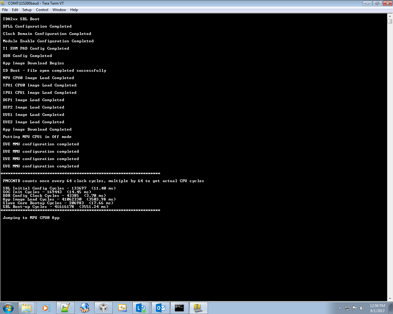
One of our customer have designed TDA2x based customized hardware. In that TDA2x customized target hardware they are using dual memory interface (SBLLIB_DUAL_EMIF_1GB_512MB ). After doing the changes listed in the attached file we are able to run the AppImage on both EVM and customer's TDAx based customized hardware.

When we tried allocating the memory in non cached section with this new configuration we are getting “MDMA error” which we were getting for single memory interface (SBLLIB_SINGLE_EMIF_512MB),

kindly help.

Regards

SocratesTargetBoardModification.xlsx

  • Hi Socrates,

    What is the starterware release that you are using?

    Regards,
    Rishabh
  • Hi Rishabh,

    We work on starterware_01_06_00_16 and Vision SDK 2.10.

    Regards,
    Socrates
  • Hi Socrates,

    Can you tell me the AMMU and LISA map configuration that you are using.
    Also what is the address in 0xB* region you are trying to allocate that gives MDMA error?

    Regards,
    Rishabh

  • Hi Rishabh,

    PFA AMMU configuration file and below is the lisa map configuration that we are using
    /* MA_LISA_MAP_i */
    HW_WR_REG32(SOC_MA_MPU_CONF_REGS_BASE + LISA_MAP_0, 0x80600200U);
    HW_WR_REG32(SOC_MA_MPU_CONF_REGS_BASE + LISA_MAP_1, 0xC0500100U);
    /* DMM_LISA_MAP_i */
    HW_WR_REG32(SOC_DMM_CONF_REGS_BASE + LISA_MAP_0, 0x80600200U);
    HW_WR_REG32(SOC_DMM_CONF_REGS_BASE + LISA_MAP_1, 0xC0500100U);

    We haven’t modified both these configurations, both are default one provided by TI.

    Regards,
    SocratesAmmu1_bios.cfg

  • Hi Socrates,

    You need to modify the AMMU as this one was done for 512 MB memory map. You should map 0xA000_0000 logical to 0xA000_0000 physical address.

    Regards,
    Rishabh
  • Hi Rishabh,

    As per your recommendations, mapped 0xA000_0000 logical to 0xA000_0000 physical address. However it is not booting and prints  “Jumping to MPU CPU0 App”.

    When i revert back the changes then it is booting up properly. Please find attached screenshot with this chain.

    Thanks

    Regards
    Socrates

  • Hi Socrates,

    You have to make below changes to modify Vision SDK memory map from 512 MB to 1.5 GB (It mostly requires user to modify code sections related to address translation).
    1. VPDMA initialization
    2. A15 MMU
    3. M4 AMMU
    4. MemoryMap: code section which translates DDR3_BASE_ADDR_1 for 512MB should be commented out
    5. SBL to be built for 1.5 GB so that LISA map is set correctly.

    Can you please refer to Memory Map document(VisionSDK_UserGuide_MemoryMap.pdf) from Vision SDK and make the changes accordingly.

    Regards,
    Rishabh
  • Hi Rishabh,

    As per your suggestion we have modified
    1. M4 AMMU
    2. SBL to be built for 1.5 GB

    We could not get much information on the following
    3. VPDMA Initialization
    4. A15 MMU and
    5. MemoryMap


    Could you please provide more insights on (3), (4) and (5) on where to make the changes in the VSDK?

    Thanks

    Best Regards
    Socrates
  • Hi Socrates,

    Please find the information below:

    1. VPDMA:

    You will map 0xA000_0000 to 0xA000_0000, hence address translation should be false.

    In ti_components\drivers\<bsp>\src\vps\src\vpsdrv_init.c make the below change:

    vpsLibInitPrms.isAddrTransReq  = FALSE;

    2. A15 MMU:

    0xA000_0000 mapping should be changed to one to one map. In vision_sdk\src\main_app\tda2xx\a15_0\a15_0.cfg, make the below change:

    for (var i=0xA0000000; i < 0xC0000000; i = i + 0x00200000) {
        // Each 'BLOCK' descriptor entry spans a 2MB address range
        Mmu.setSecondLevelDescMeta(i, i, attrs2);
    }

    3. Memory Map

    Code section which translates DDR3_BASE_ADDR_1 for 512MB should be commented out (DDR3_BASE_ADDR_1 = DDR3_BASE_ADDR_1+512*MB). Relevant changes should be made in xs file

    Regards,

    Rishabh

  • Hi Rishabh,

    Changes were made as per your suggestion. However MDMA error is not resolved yet.

    Please find attached error logs.

    Are the below changes correct? Please advise.

    1) M4 AMMU:

    Path: ..\vision_sdk\src\main_app\tda2xx\ipu1_0

    File Name: Ammu1_bios.cfg and

    Line No: 212

    Previous:
    entry.logicalAddress = 0xA0000000;
    entry.translatedAddress = 0x80000000;
                   
    Present:
    entry.logicalAddress = 0xA0000000;
    entry.translatedAddress = 0xA0000000;
                   

    2) SBL to be built for 1.5 GB so that LISA map is set correctly

    Path: ..\vision_sdk\build\makerules
                   
    File Name: build_sbl.mk
                   
    Line No: 46

    SBL_TDA2XX_OPTIONS= $(SBL_COMMON_OPTIONS) PLATFORM=tda2xx EMIFMODE=DUAL_EMIF_1GB_512MB FORCE_OPPMODE=TRUE OPPMODE=opp_nom PM_OPTIMIZE=TRUE

    Thanks

    Regards

    Socrates

  • Hi Socrates,

    Can you share the other changes as well i.e. A15 MMU and memory map.
    Thanks.

    Regards,
    Rishabh
  • Hi Rishabh,

    As stated in one of your previous reply, we updated A15 MMU and memory map.

    Regards
    Socrates
  • Hi Socrates,

    Can you share the xs file that has memory map changes.

    Regards,
    Rishabh
  • Hi Rishabh,

    Please find attached files.


    #1)

    Changes in config_m4.bld file (line no 18)

    if(A15TargetOS == "Bios")
    {
        var MemSegDefine = xdc.loadCapsule("mem_segment_definition_1024mb_bios.xs");
    }
    In the above code section 1024mb.xs MemoryMapChanges.zipfile is called.


    #2)

    Changes in Ruled,mk (Line no:212)

    ifeq ($(PLATFORM), tda2xx-evm)
    ifeq ($(DDR_MEM), )
      DDR_MEM := DDR_MEM_1024M
    endif
    endif

    The DDR_MEM_512M changed to DDR_MEM1024M.


    Thanks

    Regards
    Socrates

  • Hi Socrates,

    You want to use 1 GB or 1.5 GB? I thought the thread was about 1.5 GB. Can you please refer to the attached file 

    mem_segment_definition_1_5gb_bios.xs.txt
    Fullscreen
    1
    2
    3
    4
    5
    6
    7
    8
    9
    10
    11
    12
    13
    14
    15
    16
    17
    18
    19
    20
    21
    22
    23
    24
    25
    26
    27
    28
    29
    30
    31
    32
    33
    34
    35
    36
    37
    38
    39
    40
    41
    42
    43
    44
    45
    46
    47
    48
    49
    50
    51
    52
    53
    54
    55
    56
    57
    58
    59
    60
    61
    62
    63
    64
    65
    66
    67
    /*
    *******************************************************************************
    *
    * Copyright (C) 2013 Texas Instruments Incorporated - http://www.ti.com/
    * ALL RIGHTS RESERVED
    *
    *******************************************************************************
    */
    /*
    * ======== mem_segment_definition.xs ========
    * ======== Single file for the memory map configuration of all cores =========
    */
    function getMemSegmentDefinition_external(core)
    {
    KB=1024;
    MB=KB*KB;
    DDR3_ADDR = 0x80000000;
    DDR3_SIZE = (1024+512)*MB;
    /*
    * In case of ECC_FFI_INCLUDE, DDR3_BASE_ADDR_1 and DDR3_BASE_SIZE_1
    * are hard-coded in as values of gIpcNonCachedDataAddr and
    * gIpcNonCachedDataSize in Ipu1_0.cfg
    * If this DDR3_BASE_SIZE_0 is changed, update Ipu1_0.cfg
    */
    DDR3_BASE_ADDR_0 = DDR3_ADDR;
    DDR3_BASE_SIZE_0 = 1008*MB;
    /* The start address of the second mem section should be 16MB aligned.
    * This alignment is a must as a single 16MB mapping is used for EVE
    * to map SR0, REMOTE_LOG_MEM sections.
    * tlb_config_eveX.c need to be modified otherwise
    */
    DDR3_BASE_ADDR_1 = DDR3_BASE_ADDR_0 + DDR3_BASE_SIZE_0;
    DDR3_BASE_SIZE_1 = DDR3_SIZE - DDR3_BASE_SIZE_0;
    if(core=="ipu1_1" || core=="ipu1_0" || core=="ipu2" || core=="a15_0")
    {
    /* for ipu1_0, ipu1_1, ipu2 DDR3_BASE_ADDR_1 should be
    * in non-cached virtual address of
    * DDR3_BASE_ADDR_1 + 512*MB
    */
    // DDR3_BASE_ADDR_1 = DDR3_BASE_ADDR_1+512*MB;
    }
    DSP1_L2_SRAM_ADDR = 0x40800000;
    DSP1_L2_SRAM_SIZE = 288*KB;
    DSP2_L2_SRAM_ADDR = 0x41000000;
    DSP2_L2_SRAM_SIZE = 288*KB;
    EVE1_SRAM_ADDR = 0x42000000;
    EVE1_SRAM_SIZE = 1*MB;
    EVE2_SRAM_ADDR = 0x42100000;
    EVE2_SRAM_SIZE = 1*MB;
    EVE3_SRAM_ADDR = 0x42200000;
    EVE3_SRAM_SIZE = 1*MB;
    EVE4_SRAM_ADDR = 0x42300000;
    EVE4_SRAM_SIZE = 1*MB;
    TOTAL_MEM_SIZE = (DDR3_SIZE);
    XXXXXXXXXXXXXXXXXXXXXXXXXXXXXXXXXXXXXXXXXXXXXXXXXX
    and analyze the differences and then try.

    Regards,

    Rishabh