This thread has been locked.

If you have a related question, please click the "Ask a related question" button in the top right corner. The newly created question will be automatically linked to this question.

AM5749: AM574x Datasheet Timing Diagram Formulas

Part Number: AM5749

Hello,

I'm planning to interface a custom board with an AM5749 GPMC peripheral to an FPGA with the FPGA interface emulating an asynchronous non-multiplexed NOR flash-like interface.

I'm looking at the timing diagrams in the datasheet (sprs982h) and I'm a little confused about the formulas.

For example, from Table 5-61, for FA9, the footnote (5) for value J shows the formula:

(5) J = (CSOnTime × (TimeParaGranularity + 1) + 0.5 × CSExtraDelay) × GPMC_FCLK

This doesn't seem to make sense, since the timings are shown in units of ns.

The CSOnTime register is in units of GPMC_FCLK cycles, the TimeParaGranularity register is a scalar multiplier that can be set to 1 or 2 and the CSExtraDelay register can be set to 0 or 1 to enable the extra 0.5 clock cycle delay.

In the formula, should GPMC_FCLK be the period of GPMC_FCLK or am I not understanding how it works correctly?

Thanks,

USO

  • Hi USO,

    You are correct - in the formula use the period of GPMC_FCLK in ns.

    The GPMC uses the internal GPMC_FCLK clock to increment counters that determine the GPMC timings. The bitfields in the GPMC_CONFIG# registers compare against the count of GPMC_FCLK cycles to control the timings of signals and other events like read access time, etc.

    This is true when GPMC is configured for synchronous or asynchronous mode.
    In synchronous mode the GPMC_FCLK (or some divided version of it) is output on the GPMC_CLK pin.
    In asynchronous mode, the GPMC_FCLK is still used to increment the counters that control timings, but the GPMC_CLK pin is static low - GPMC is not internally asynchronous.

    CSOnTime determines the number of GPMC_FCLK cycles from the beginning of the GPMC access to when CS becomes active (it can be configured active high or active low).

    The CSOnTime bitfield is 4-bits, so the counter of GPMC_FCLK cycles can go up to 15 decimal. This is true of many of the bitfields that control timings of other signals. If any of these timing require more than 15 GPMC_FCLK cycles, you could slow down the GPMC_FCLK going into the GPMC or you can use TIMEPARAGRANULARITY to increment the GPMC_FCLK count every other GPMC_FCLK cycle - doubling the time from the beginning of the GPMC access to the event (CSOnTime in this case).

    Finally the CSExtraDelay parameter delays the CSOnTime and CSOffTime by 1/2 GPMC_FCLK cycle - launching on the falling edge of GPMC_FCLK instead of the rising edge. This offers yet more configurability for the GPMC signals to meet desired timings.

    In summary, every GPMC timing is clocked by the GPMC_FCLK internal clock even in asynchrnous mode. There is a tradeoff between GPMC cycle time and resolution of signal timings. A faster GPMC_FCLK allows for more signal transitions per unit time, but limits the maximum time of a GPMC cycle.

    Its best to think of timings in terms of GPMC_FCLK cycles whether synchronous or asynchronous.

    To trace the source of the GPMC_FCLK clock, I recommend using the Clock Tree Tool for Sitara, Automotive, Vision Analytics, & Digital Signal Processors. I believe the default GPMC_FCLK on this device may be 266MHz.

    Hope this helps,
    Mark

  • Hi Mark,

    Thank you very much for your detailed response.

    I'm planning to leave the GPMC_FCLK at 266MHz.

    My FPGA will be limited to 100MHz due to limitations from other logic in the device.

    The AM5749 and the FPGA are clocked from separate oscillators, so the two devices will be under totally different clock domains, so timing may be a little bit tricky since the clocks could drift relative to each other and the clock ratio is not a nice multiple.

    I'm planning to use the CS active edge to trigger the FPGA to latch the address, since our custom board HW does not have the nADV line connected :(

    I think that should still work though since I think I can set the GPMC timing up with the CSOnTime so the address should already be valid by the time the CS is asserted + latency in the FPGA from using 2x synchronizer flip flops on CS. From this I shouldn't have to worry about setup time in the FPGA.

    From the timing diagrams, it looks like the GPMC drives the address bus throughout the transaction for both single reads and writes. Then I shouldn't have to worry about hold timing in the FPGA. Is this correct?

    After the FPGA latches the address, the FPGA will assert the WAIT signal as a sort of handshake, so the GPMC can latch data at the right time for a single read and hold the data for long enough for a single write.

    I'll also use 2x synchronizer flip flops for the nOE and nWE control signals for single reads and writes to address metastability. If I set up the GPMC timing registers appropriately, hopefully that can account for all the different possible GPMC_FCLK to FPGA clock edge scenarios without metastability, data coherency or data loss issues.

    Any thoughts or advice you could provide regarding my interfacing plan?

    From the timing diagram formulas, it looks like the GpmcFclkDivider does not affect any of the timings in asynchronous mode, so if I need more time, the only way is to use the TimeParaGranularity register eh?
    I'd rather not have to slow down the GPMC_FCLK as it's also shared with other subsystems in the CPU.

    One more thing, I'm looking at the Datasheet timing diagram in Figure 5-30, and the diagram shows FA14 and FA15, but I can't find any corresponding values for FA14 and FA15 anywhere else in the datasheet. Do you know what those values are?

    Thanks again,

    USO

  • Hi USO,

    Drift is a valid concern. You might have to stretch out the asynchronous GPMC timings to ensure timings can be met.

    The AM5749 can route the GPMC_FCLK (input clock to GPMC peripheral) to GPIO6_16.clkout1 with possible clock dividers. The intention is to provide a free-running version of the GPMC_CLK that can be used for synchronous mode. In that scenario, to keep in phase with the GPMC_CLK, the clkout1 mux must be in divide-by-1 mode. The datasheet provides a skew from the GPMC_CLK to this clkout1 pin (a delay of 0.96ns to 6.1ns). Timing closure should allow upto maybe 80MHz depending on the other device's max output delay and min hold time.

    Anyway, you might be able to utilize this clkout1 as a reference clock to the FPGA to avoid CLK drift. I don't expect it to look very pretty at 266MHz, so it would have to be divided. The divided clock will have an uncontrollable phase offset to the start of the GPMC cycle. For example if divided-by-2, the start of the GPMC cycle might occur when the clkout1 is going high. But after a reboot the start of the GPMC cycle could occur when the clkout is going low. Maybe it helps you?

    =-=-=-

    It should be fine to use CS to latch the address with CSOnTime. In non-mux mode, the address is valid on the address bus throughout the GPMC cycle.

    =-=-=-

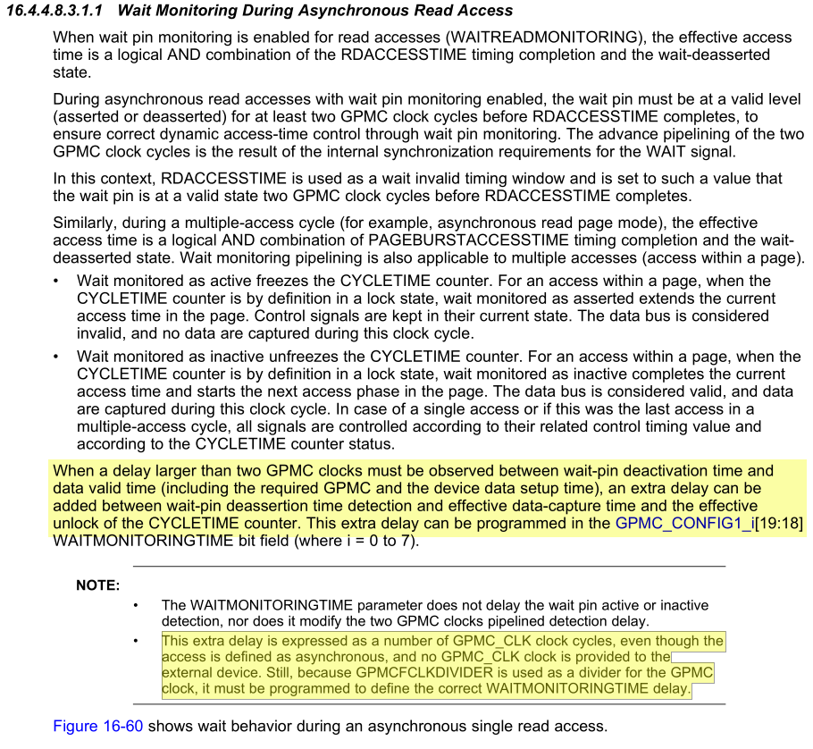
    GpmcFclkDivider actually does get used in asynch mode when latching WAIT inputs with WaitMonitoringTime > 0 - ie you need more than 2 GPMC_FCLK cycles from WAIT to data valid on bus (reads) or data latched by FPGA (writes). But GpmcFclkDivider does not alter the timings of the ONTIME/OFFTIME timings (CS,ADV,WE,OE). TimeParaGranularity can stretch their timings by a factor of 2. *EXTRADELAY can cause the ONTIME/OFFTIME to launch 1/2 GPMC_FCLK cycle later. You can slow the input clock to GPMC if the peripherals sharing it can still operate.

    Check out TRM 16.4.4.8.3.1.1 Wait Monitoring During Asynchronous Read Access
    And TRM 16.4.4.8.3.1.2 Wait Monitoring During Asynchronous Write Access
    AM574x Technical Reference Manual (Rev. B)

    Make sure to setup WRACCESSTIME and RDACCESSTIME to be at least 2 GPMC_FLCK cycles after your WAIT signal is valid (asserted either high or low after the address latch)

    =-=-=-

    FA14 and FA15 are timings for the GPMC_DIR signal which is not routed to any pin on AM5749. They're removed from the table, but were kept in Figure 5-30 from a previous datasheet.

    Hope this helps,
    Mark

  • Hi Mark,

    Thanks again for the detailed response.

    • In my single read timing diagram (attached), I've made sure to account for the 2 GPMC_FCLK cycles needed for the WAIT line.
      • The FPGA will assert the WAIT signal at least 2 GPMC_FCLK cycles before RdAccessTime so the signal transition is not missed by the GPMC due to the 2x synchronizer delay in the AM5749 internal GPMC WAIT data path.
      • Since the WAIT pin will already be asserted when the AM5749 starts monitoring the WAIT pin, it should dynamically extend the effective read access time to compensate for possible timing differences cycle to cycle between the two devices.
      • When data is driven on the data bus by the FPGA, the FPGA will then deassert the WAIT signal and min. 2 GPMC_FCLK cycles after the deassertion, the AM5749 should latch the data on the bus if my understanding is correct.
      • I'll need to ensure the FPGA holds the data on the bus long enough that the GPMC can latch the data.

    One last question:

    • Regarding GPMC_DIR, I realize the signal is not routed to any pin, but I need to know when the GPMC tri-states the data bus to avoid bus contention.
    • Since FA14 and FA15 are not provided, can I assume the data bus tristate timing follows OEn assertion and deassertion timing (FA13 and FA4)?

    Thanks again for your help,

    USO

    gpmc_test_fpga_timing_v0.0.1.pdf

  • Hi USO,

    Your WAIT handshaking seems fine.

    I'm checking with the design team to see how you should use the OEn signal to avoid data bus contention.

    Obviously while OEn is driven low, the GPMC data pins should be inputs to receive the data being read. But the datasheet drawings show that the DIR pin stays high (IN) after the OEn rise edge until the end of the cycle.

    I hope to have a response in a couple of days and will get back to you.

    Regards,
    Mark

  • Hi Mark,

    Any update on this?

    Thanks,

    USO

  • Hi USO,

    The designer provided the below explanation...

    The DIR signal will go from high (IN) to low (out) after RdCycleTime has elapsed. This DIR signal is for controlling the external buffer on the board. Typically, if the external memory is connected directly to the GPMC pins, then you don’t need the DIR signal. The memory device will use OE to drive/not-drive the data.

    Typically, the external memory device will start driving read data some time after OE is asserted low. The GPMC then latches the read data on OE transitioning high (RdAccessTime). Then the external memory stops driving the data some time after OE has been deasserted high. The RdCycleTime is programmable, so must include the time it takes the external memory (in this case FPGA) to stop driving the data. This will ensure that there is no contention on the data bus.


    =-=-=-

    OEn is the signal that tells the memory/FPGA that it can drive the data bus.
    My concern was with meeting hold time after OEn goes high if the data bus goes high-Z immediately when OEn goes high (if READACCESSTIME = OENOFFIME).
    Looking at actual memory devices (CY7C10612G for example), the memory appears to drive the DATA bus after OEn goes high. But there is no minimum time after OEn specified - only max time.
    In reality the GPMC latches the data bus when its internal count of GPMC_FCLK cycles reaches READACCESSTIME, not when OEn goes high.
    If you set READACCESSTIME < OENOFFTIME, it will be fine to use OEn (and not DIR) to tell the FPGA when to get on/off the data bus.

    During a read, you could also have the FPGA drive the data bus from OEn going low until CS goes high.

    Regards,
    Mark

  • Thanks Mark,

    That answers my question.

    Since the GPMC will hold the bus in high-Z for RdCycleTime duration, that works well.

    I'm going to set up the GPMC CSOffTime = OEOffTime and RdCycleTime to be longer; long enough to account for the slower FPGA clock 2 cycle delay from 2x input synchronizers, so that the FPGA will stop driving the data before the next GPMC read/write cycle starts. The two cycle FPGA clock delay from deassertion of CSn and OEn will give plenty of time for the GPMC to latch the data so I won't have to worry about the hold time.

    Thanks for the wonderful support!

  • Hi Mark,

    Just wanted to let you know we were able to get single reads and writes working between the AM5749 and an FPGA with your clarifications :)

    The only problem now is my colleague tells me the accesses are slow.

    He is only using a for loop to perform multiple single read accesses.

    I worked on the FPGA side of things and he is working on the AM5749 side of things. He is using the DSP core to access the GPMC.

    Is there a faster way to do multiple single read accesses consecutively?

    Our cycle2cycledelay is set to 0, so from the documentation I think we should be able to perform back-to-back 16-bit word single read cycles with no delay in between each access. For example, the last GPMC FCLK cycle of the first read cycle should also be the first GPMC FCLK cycle of the following read cycle.

    How do we "queue" multiple successive single read accesses?

    Is DMA the way to do it or is there another way?

    Or will there be some inherent delay between successive single read cycles?

    I know we can use multiple reads (page mode) to speed things up as well, but that's a next development step. But following my questions for single reads, for multiple reads, will there also be some inherent delay between consecutive multiple reads (page mode) since the page size is limited to max 16 words? In other words will there be delay between successive 16 word multiple reads (page mode).

    Thanks,

    Udell

  • Hi Udell,

    Great to hear!

    Using the DMA with single access (WriteMultiple = ReadMultiple = 0) improves the throughput quite a bit by reducing the time between consecutive transfers.

    You can see this to a limited extent by using 32-bit pointers instead of 16-bit (or 8-bit pointers) to the GPMC memory mapped region. On a 16-bit bus, a 32-bit access will perform back to back 16-bit transfers with no delay between the 2 accesses. This does not scale beyond 32-bits (ie 64-bit wont offer 4 back to back 16-bit transfers).

    I recommend using the DMA  as an intermediate step before the FPGA supports page mode. Page reads (ReadMultiple set) can dramatically improve throughput. Asynch page writes are not supported - the signals will come out as if WriteMultiple is not set. But synchronous burst writes are supported by GPMC (address bus does not change for each word of the burst like asynch page read).

    Can you measure the delays between GPMC accesses with a scope or logical analyzer?

    Regards,
    Mark

  • Hi Mark,

    I think we will get the DMA working next, but I'll ask my colleague to get some screenshots of the delays he's seeing when just using CPU accesses with a "for loop".

    We may recut the HW to connect the gpmc_clk and gpmc_advn_ale lines in the future, so we have the option to do asynchronous or synchronous transfers if we need even higher throughput. Always best to have the option to upgrade the performance, so we have more time for our control loop.

    Asynchronous page mode and synchronous burst mode are still limited to 16 words max right?

    In between each 16 word burst, there will be some delay even if we use DMA?

    Best Regards,

    Udell

  • Hi Udell,

    Yes, 16-word burst is the max.

    Regards,
    Mark

  • Hi Mark,

    Just wanted to give an update in case this might help somebody else. We were able to get the DMA working and improved the timing considerably.

    We were able to do 64 16-bit words with consecutive single writes in ~3.4us and with consecutive single reads in ~7.6us.

    The timing could be optimized a bit more by small adjustments to the GPMC timing register settings, but the performance was acceptable for us for now.

    Timing is also limited since our AM5749 external clock and FPGA clock are not from the same crystal/clock driver so 2x flip-flop synchronizers on the GPMC control lines add a lot of delay and the FPGA clock is limited to 100MHz compared to the GPMC FCLK at 266MHz.

    For further improvements, we will likely change the HW and use a synchronous interface instead asynchronous.

    One critical thing I had to account for was when the GPMC started to monitor the WAIT pin at RdAccessTime/WrAccessTime and WAIT was asserted, the GPMC FCLK internal counter would freeze and then two GPMC FCLK cycles after WAIT was deasserted (due to GPMC internal synchronizers), the counter would unfreeze, and start incrementing the counter again on the next GPMC FCLK cycle. At the start, I wasn't sure how that would behave.

    Thanks for you all your help!