


Other Parts Discussed in Thread: OMAPL138
Tool/software: Code Composer Studio
Hi sir,
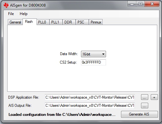
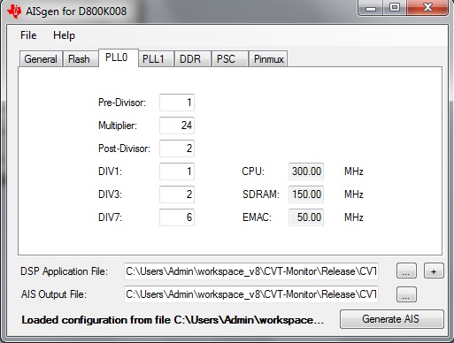
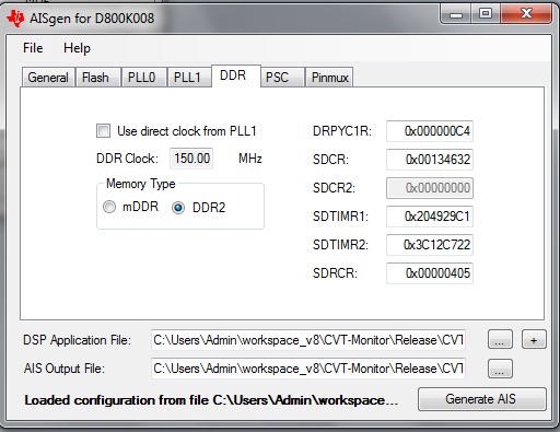
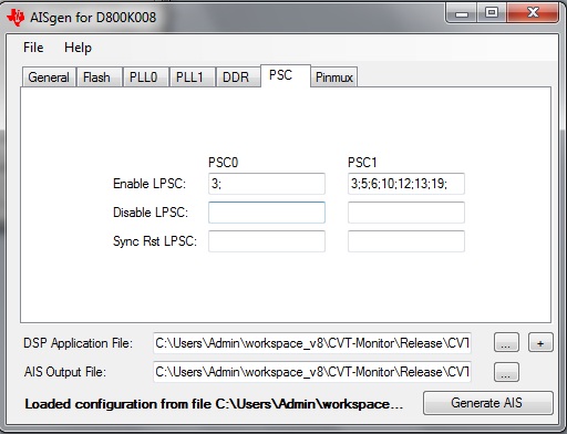
I am using TMS320C6748 DSP with External NOR Flash using.
Actually in .cmd file DSPL2RAM i used it is booting from NOR FLASH, when i will change to DDR2 in .cmd it's not booting.
In AIS Gen all settings given properly please could you give me some suggestions.
below i am attaching AIS Gen setting images and (whatever in Debug mode DDR2 worked fine used) OMAPL138_LCDK.gel attaching.


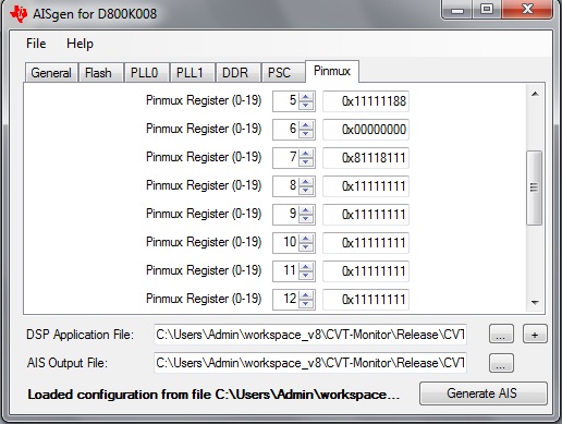
and i am attaching my gel(OMAPL138_LCDK) file also sir,
#define PLL0_BASE 0x01C11000 /*SYSTEM PLL BASE ADDRESS*/
#define PLL0_PID *(unsigned int*) (PLL0_BASE + 0x00) /*PID*/
#define PLL0_RSTYPE *(unsigned int*) (PLL0_BASE + 0xE4) /*Reset Type status Reg*/
#define PLL0_PLLCTL *(unsigned int*) (PLL0_BASE + 0x100) /*PLL Control Register*/
#define PLL0_OCSEL *(unsigned int*) (PLL0_BASE + 0x104) /*OBSCLK Select Register*/
#define PLL0_SECCTL *(unsigned int*) (PLL0_BASE + 0x108) /*PLL Secondary Control Register*/
#define PLL0_PLLM *(unsigned int*) (PLL0_BASE + 0x110) /*PLL Multiplier*/
#define PLL0_PREDIV *(unsigned int*) (PLL0_BASE + 0x114) /*Pre divider*/
#define PLL0_PLLDIV1 *(unsigned int*) (PLL0_BASE + 0x118) /*Divider-1*/
#define PLL0_PLLDIV2 *(unsigned int*) (PLL0_BASE + 0x11C) /*Divider-2*/
#define PLL0_PLLDIV3 *(unsigned int*) (PLL0_BASE + 0x120) /*Divider-3*/
#define PLL0_OSCDIV1 *(unsigned int*) (PLL0_BASE + 0x124) /*Oscilator Divider*/
#define PLL0_POSTDIV *(unsigned int*) (PLL0_BASE + 0x128) /*Post Divider*/
#define PLL0_BPDIV *(unsigned int*) (PLL0_BASE + 0x12C) /*Bypass Divider*/
#define PLL0_WAKEUP *(unsigned int*) (PLL0_BASE + 0x130) /*Wakeup Reg*/
#define PLL0_PLLCMD *(unsigned int*) (PLL0_BASE + 0x138) /*Command Reg*/
#define PLL0_PLLSTAT *(unsigned int*) (PLL0_BASE + 0x13C) /*Status Reg*/
#define PLL0_ALNCTL *(unsigned int*) (PLL0_BASE + 0x140) /*Clock Align Control Reg*/
#define PLL0_DCHANGE *(unsigned int*) (PLL0_BASE + 0x144) /*PLLDIV Ratio Chnage status*/
#define PLL0_CKEN *(unsigned int*) (PLL0_BASE + 0x148) /*Clock Enable Reg*/
#define PLL0_CKSTAT *(unsigned int*) (PLL0_BASE + 0x14C) /*Clock Status Reg*/
#define PLL0_SYSTAT *(unsigned int*) (PLL0_BASE + 0x150) /*Sysclk status reg*/
#define PLL0_PLLDIV4 *(unsigned int*) (PLL0_BASE + 0x160) /*Divider 4*/
#define PLL0_PLLDIV5 *(unsigned int*) (PLL0_BASE + 0x164) /*Divider 5*/
#define PLL0_PLLDIV6 *(unsigned int*) (PLL0_BASE + 0x168) /*Divider 6*/
#define PLL0_PLLDIV7 *(unsigned int*) (PLL0_BASE + 0x16C) /*Divider 7*/
#define PLL0_PLLDIV8 *(unsigned int*) (PLL0_BASE + 0x170) /*Divider 8*/
#define PLL0_PLLDIV9 *(unsigned int*) (PLL0_BASE + 0x174) /*Divider 9*/
#define PLL0_PLLDIV10 *(unsigned int*) (PLL0_BASE + 0x178) /*Divider 10*/
#define PLL0_PLLDIV11 *(unsigned int*) (PLL0_BASE + 0x17C) /*Divider 11*/
#define PLL0_PLLDIV12 *(unsigned int*) (PLL0_BASE + 0x180) /*Divider 12*/
#define PLL0_PLLDIV13 *(unsigned int*) (PLL0_BASE + 0x184) /*Divider 13*/
#define PLL0_PLLDIV14 *(unsigned int*) (PLL0_BASE + 0x188) /*Divider 14*/
#define PLL0_PLLDIV15 *(unsigned int*) (PLL0_BASE + 0x18C) /*Divider 15*/
#define PLL0_PLLDIV16 *(unsigned int*) (PLL0_BASE + 0x190) /*Divider 16*/
#define PLL1_BASE 0x01E1A000 /*SYSTEM PLL1 BASE ADDRESS*/
#define PLL1_PID *(unsigned int*) (PLL1_BASE + 0x00) /*PID*/
#define PLL1_RSTYPE *(unsigned int*) (PLL1_BASE + 0xE4) /*Reset Type status Reg*/
#define PLL1_PLLCTL *(unsigned int*) (PLL1_BASE + 0x100) /*PLL Control Register*/
#define PLL1_OCSEL *(unsigned int*) (PLL1_BASE + 0x104) /*OBSCLK Select Register*/
#define PLL1_SECCTL *(unsigned int*) (PLL1_BASE + 0x108) /*PLL Secondary Control Register*/
#define PLL1_PLLM *(unsigned int*) (PLL1_BASE + 0x110) /*PLL Multiplier*/
#define PLL1_PREDIV *(unsigned int*) (PLL1_BASE + 0x114) /*Pre divider*/
#define PLL1_PLLDIV1 *(unsigned int*) (PLL1_BASE + 0x118) /*Divider-1*/
#define PLL1_PLLDIV2 *(unsigned int*) (PLL1_BASE + 0x11C) /*Divider-2*/
#define PLL1_PLLDIV3 *(unsigned int*) (PLL1_BASE + 0x120) /*Divider-3*/
#define PLL1_OSCDIV1 *(unsigned int*) (PLL1_BASE + 0x124) /*Oscilator Divider*/
#define PLL1_POSTDIV *(unsigned int*) (PLL1_BASE + 0x128) /*Post Divider*/
#define PLL1_BPDIV *(unsigned int*) (PLL1_BASE + 0x12C) /*Bypass Divider*/
#define PLL1_WAKEUP *(unsigned int*) (PLL1_BASE + 0x130) /*Wakeup Reg*/
#define PLL1_PLLCMD *(unsigned int*) (PLL1_BASE + 0x138) /*Command Reg*/
#define PLL1_PLLSTAT *(unsigned int*) (PLL1_BASE + 0x13C) /*Status Reg*/
#define PLL1_ALNCTL *(unsigned int*) (PLL1_BASE + 0x140) /*Clock Align Control Reg*/
#define PLL1_DCHANGE *(unsigned int*) (PLL1_BASE + 0x144) /*PLLDIV Ratio Chnage status*/
#define PLL1_CKEN *(unsigned int*) (PLL1_BASE + 0x148) /*Clock Enable Reg*/
#define PLL1_CKSTAT *(unsigned int*) (PLL1_BASE + 0x14C) /*Clock Status Reg*/
#define PLL1_SYSTAT *(unsigned int*) (PLL1_BASE + 0x150) /*Sysclk status reg*/
#define PLL1_PLLDIV4 *(unsigned int*) (PLL1_BASE + 0x160) /*Divider 4*/
#define PLL1_PLLDIV5 *(unsigned int*) (PLL1_BASE + 0x164) /*Divider 5*/
#define PLL1_PLLDIV6 *(unsigned int*) (PLL1_BASE + 0x168) /*Divider 6*/
#define PLL1_PLLDIV7 *(unsigned int*) (PLL1_BASE + 0x16C) /*Divider 7*/
#define PLL1_PLLDIV8 *(unsigned int*) (PLL1_BASE + 0x170) /*Divider 8*/
#define PLL1_PLLDIV9 *(unsigned int*) (PLL1_BASE + 0x174) /*Divider 9*/
#define PLL1_PLLDIV10 *(unsigned int*) (PLL1_BASE + 0x178) /*Divider 10*/
#define PLL1_PLLDIV11 *(unsigned int*) (PLL1_BASE + 0x17C) /*Divider 11*/
#define PLL1_PLLDIV12 *(unsigned int*) (PLL1_BASE + 0x180) /*Divider 12*/
#define PLL1_PLLDIV13 *(unsigned int*) (PLL1_BASE + 0x184) /*Divider 13*/
#define PLL1_PLLDIV14 *(unsigned int*) (PLL1_BASE + 0x188) /*Divider 14*/
#define PLL1_PLLDIV15 *(unsigned int*) (PLL1_BASE + 0x18C) /*Divider 15*/
#define PLL1_PLLDIV16 *(unsigned int*) (PLL1_BASE + 0x190) /*Divider 16*/
/*PSC Module Related Registers*/
#define PSC0_BASE 0x01C10000
#define PSC1_BASE 0x01E27000
#define PSC0_MDCTL (PSC0_BASE+0xA00)
#define PSC0_MDSTAT (PSC0_BASE+0x800)
#define PSC0_PTCMD *(unsigned int*) (PSC0_BASE + 0x120)
#define PSC0_PTSTAT *(unsigned int*) (PSC0_BASE + 0x128)
#define PSC1_MDCTL (PSC1_BASE+0xA00)
#define PSC1_MDSTAT (PSC1_BASE+0x800)
#define PSC1_PTCMD *(unsigned int*) (PSC1_BASE + 0x120)
#define PSC1_PTSTAT *(unsigned int*) (PSC1_BASE + 0x128)
#define PSC_TIMEOUT 200 // This value can be optimized by the user
#define LPSC_EDMA_CC0 0
#define LPSC_EDMA_TC0 1
#define LPSC_EDMA_TC1 2
#define LPSC_EMIFA 3 /*PSC0*/
#define LPSC_SPI0 4 /*PSC0*/
#define LPSC_MMCSD0 5 /*PSC0*/
#define LPSC_ARM_AINTC 6
#define LPSC_ARM_RAMROM 7 /*PSC0*/
// LPSC #8 not used
#define LPSC_UART0 9 /*PSC0*/
#define LPSC_SCR0 10
#define LPSC_SCR1 11
#define LPSC_SCR2 12
// LPSC #13 not used
#define LPSC_ARM 14 /*PSC0*/
#define LPSC_DSP 15 /*PSC0*/
#define LPSC_EDMA_CC1 0
#define LPSC_USB20 1 /*PSC1*/
#define LPSC_USB11 2 /*PSC1*/
#define LPSC_GPIO 3 /*PSC1*/
#define LPSC_UHPI 4 /*PSC1*/
#define LPSC_EMAC 5 /*PSC1*/
#define LPSC_DDR 6 /*PSC1*/
#define LPSC_MCASP0 7 /*PSC1*/
#define LPSC_SATA 8 /*PSC1*/
#define LPSC_VPIF 9 /*PSC1*/
#define LPSC_SPI1 10 /*PSC1*/
#define LPSC_I2C1 11 /*PSC1*/
#define LPSC_UART1 12 /*PSC1*/
#define LPSC_UART2 13 /*PSC1*/
#define LPSC_MCBSP0 14 /*PSC1*/
#define LPSC_MCBSP1 15 /*PSC1*/
#define LPSC_LCDC 16 /*PSC1*/
#define LPSC_EPWM 17 /*PSC1*/
#define LPSC_MMCSD1 18
#define LPSC_UPP 19
#define LPSC_ECAP 20
#define LPSC_EDMA_TC2 21
// LPSC #22-23 not used
#define LPSC_SCR_F0 24
#define LPSC_SCR_F1 25
#define LPSC_SCR_F2 26
#define LPSC_SCR_F6 27
#define LPSC_SCR_F7 28
#define LPSC_SCR_F8 29
#define LPSC_BR_F7 30
#define LPSC_SHARED_RAM 31
/*DDR MMR Declaration*/
#define VTPIO_CTL *(unsigned int*)(0x01E2C000) // VTPIO_CTL Register
#define EMIFDDR_SDRAM_CFG 0xB0000000
#define EMIFDDR_REVID *(unsigned int*)(EMIFDDR_SDRAM_CFG + 0x00) //EMIF Module ID and Revision Register
#define EMIFDDR_SDRSTAT *(unsigned int*)(EMIFDDR_SDRAM_CFG + 0x04) //SDRAM Status Register
#define EMIFDDR_SDCR *(unsigned int*)(EMIFDDR_SDRAM_CFG + 0x08) //SDRAM Bank Config Register
#define EMIFDDR_SDRCR *(unsigned int*)(EMIFDDR_SDRAM_CFG + 0x0C) //SDRAM Refresh Control Register
#define EMIFDDR_SDTIMR1 *(unsigned int*)(EMIFDDR_SDRAM_CFG + 0x10) //SDRAM Timing Register1
#define EMIFDDR_SDTIMR2 *(unsigned int*)(EMIFDDR_SDRAM_CFG + 0x14) //SDRAM Timing Register2
#define EMIFDDR_SDCR2 *(unsigned int*)(EMIFDDR_SDRAM_CFG + 0x1C) //SDRAM Config Register2
#define EMIFDDR_PBBPR *(unsigned int*)(EMIFDDR_SDRAM_CFG + 0x20) //VBUSM Burst Priority Register
#define EMIFDDR_VBUSMCFG1 *(unsigned int*)(EMIFDDR_SDRAM_CFG + 0x28) //VBUSM config Value1 Register
#define EMIFDDR_VBUSMCFG2 *(unsigned int*)(EMIFDDR_SDRAM_CFG + 0x2C) //VBUSM config Value2 Register
#define EMIFDDR_IRR *(unsigned int*)(EMIFDDR_SDRAM_CFG + 0xC0) //Interrupt Raw Register
#define EMIFDDR_IMR *(unsigned int*)(EMIFDDR_SDRAM_CFG + 0xC4) //Interrupt Masked Register
#define EMIFDDR_IMSR *(unsigned int*)(EMIFDDR_SDRAM_CFG + 0xC8) //Interrupt Mask Set Register
#define EMIFDDR_IMCR *(unsigned int*)(EMIFDDR_SDRAM_CFG + 0xCC) //Interrupt Mask Clear Register
#define DDRPHYREV *(unsigned int*)(EMIFDDR_SDRAM_CFG + 0xE0) //DDR PHY ID and Revision Register
#define DRPYC1R *(unsigned int*)(EMIFDDR_SDRAM_CFG + 0xE4) //DDR PHY Control 1 Register
#define DDR2 0 // Do not change this value
#define MDDR 1 // Do not change this value
#define VTP_TIMEOUT 200 // This value can be optimized by the user
#define DDR_DEBUG 0 // Set this to "1" to program DDR with more timing slack
#define EMIFDDR_BASE_ADDR 0xC0000000
#define EMIFA_BASE_ADDR 0x40000000
#define EMIFA_CS2_BASE_ADDR 0x60000000
#define EMIFA_CS3_BASE_ADDR 0x62000000
#define EMIFA_CS4_BASE_ADDR 0x64000000
#define EMIFA_CS5_BASE_ADDR 0x66000000
/*EMIF2.5 MMR Declaration*/
#define EMIFA 0x68000000
#define EMIFA_AWAITCFG *(unsigned int*)(EMIFA + 0x04)
#define EMIFA_SDCFG *(unsigned int*)(EMIFA + 0x08)
#define EMIFA_SDREF *(unsigned int*)(EMIFA + 0x0C)
#define EMIFA_ACFG2 *(unsigned int*)(EMIFA + 0x10) //Async Bank1 Config Register
#define EMIFA_ACFG3 *(unsigned int*)(EMIFA + 0x14) //Async Bank2 Config Register
#define EMIFA_ACFG4 *(unsigned int*)(EMIFA + 0x18) //Async Bank3 Config Register
#define EMIFA_ACFG5 *(unsigned int*)(EMIFA + 0x1C) //Async Bank4 Config Register
#define EMIFA_SDTIM *(unsigned int*)(EMIFA + 0x20) //SDRAM Timing Register
#define EMIFA_SRPD *(unsigned int*)(EMIFA + 0x3C)
#define EMIFA_NANDFCR *(unsigned int*)(EMIFA + 0x60)
/*GPIO MMR*/
#define GPIO_REG_BASE (0x01E26000)
#define GPIO_BANK_OFFSET (0x28)
#define GPIO_DAT_OFFSET (0x04)
#define GPIO_SET_OFFSET (0x08)
#define GPIO_CLR_OFFSET (0x0C)
#define GPIO_BINTEN *(unsigned int*)(GPIO_REG_BASE + 0x08)
#define GPIO_BANK01_BASE (GPIO_REG_BASE + 0x10)
#define GPIO_BANK23_BASE (GPIO_BANK01_BASE + GPIO_BANK_OFFSET)
#define GPIO_BANK45_BASE (GPIO_BANK23_BASE + GPIO_BANK_OFFSET)
#define GPIO_BANK67_BASE (GPIO_BANK45_BASE + GPIO_BANK_OFFSET)
#define GPIO_BANK8_BASE (GPIO_BANK67_BASE + GPIO_BANK_OFFSET)
#define GPIO_BANK23_DIR *(unsigned int*)(GPIO_BANK23_BASE)
#define GPIO_BANK23_DAT *(unsigned int*)(GPIO_BANK23_BASE + GPIO_DAT_OFFSET)
#define GPIO_BANK23_SET *(unsigned int*)(GPIO_BANK23_BASE + GPIO_SET_OFFSET)
#define GPIO_BANK23_CLR *(unsigned int*)(GPIO_BANK23_BASE + GPIO_CLR_OFFSET)
/*System MMR Declaration*/
#define SYS_BASE 0x01C14000
#define HOST0CFG *(unsigned int*)(SYS_BASE + 0x040) //ARM HOST0CFG
#define KICK0R *(unsigned int*)(SYS_BASE + 0x038)
#define KICK1R *(unsigned int*)(SYS_BASE + 0x03c)
#define PINMUX0 *(unsigned int*)(SYS_BASE + 0x120) //PINMUX0
#define PINMUX1 *(unsigned int*)(SYS_BASE + 0x124) //PINMUX1
#define PINMUX2 *(unsigned int*)(SYS_BASE + 0x128) //PINMUX2
#define PINMUX3 *(unsigned int*)(SYS_BASE + 0x12C) //PINMUX3
#define PINMUX4 *(unsigned int*)(SYS_BASE + 0x130) //PINMUX4
#define PINMUX5 *(unsigned int*)(SYS_BASE + 0x134) //PINMUX5
#define PINMUX6 *(unsigned int*)(SYS_BASE + 0x138) //PINMUX6
#define PINMUX7 *(unsigned int*)(SYS_BASE + 0x13C) //PINMUX7
#define PINMUX8 *(unsigned int*)(SYS_BASE + 0x140) //PINMUX8
#define PINMUX9 *(unsigned int*)(SYS_BASE + 0x144) //PINMUX9
#define PINMUX10 *(unsigned int*)(SYS_BASE + 0x148) //PINMUX10
#define PINMUX11 *(unsigned int*)(SYS_BASE + 0x14C) //PINMUX11
#define PINMUX12 *(unsigned int*)(SYS_BASE + 0x150) //PINMUX12
#define PINMUX13 *(unsigned int*)(SYS_BASE + 0x154) //PINMUX13
#define PINMUX14 *(unsigned int*)(SYS_BASE + 0x158) //PINMUX14
#define PINMUX15 *(unsigned int*)(SYS_BASE + 0x15C) //PINMUX15
#define PINMUX16 *(unsigned int*)(SYS_BASE + 0x160) //PINMUX16
#define PINMUX17 *(unsigned int*)(SYS_BASE + 0x164) //PINMUX17
#define PINMUX18 *(unsigned int*)(SYS_BASE + 0x168) //PINMUX18
#define PINMUX19 *(unsigned int*)(SYS_BASE + 0x16C) //PINMUX19
#define CFGCHIP0 *(unsigned int*)(SYS_BASE + 0x17C)
#define CFGCHIP2 *(unsigned int*)(SYS_BASE + 0x184)
#define CFGCHIP3 *(unsigned int*)(SYS_BASE + 0x188)
#define PD0 0 /*Power Domain-0*/
#define PD1 1 /*Power Domain-1*/
#define PLLEN_MUX_SWITCH 4
#define PLL_LOCK_TIME_CNT 2400
#define PLL_STABILIZATION_TIME 2000
#define PLL_RESET_TIME_CNT 200
OnTargetConnect( )
{
GEL_TextOut("\tTarget Connected.\n","Output",1,1,1);
GEL_TextOut("\t---------------------------------------------\n","Output",1,1,1);
Clear_Memory_Map();
Setup_Memory_Map();
PSC_All_On();
Core_300MHz_mDDR_150MHz();
Wake_DSP();
}
menuitem "Wake Core"
hotmenu Wake_DSP()
{
PSC0_LPSC_enableCore(1, LPSC_DSP);
GEL_TextOut("\tDSP Wake Complete.\n","Output",1,1,1);
GEL_TextOut("\t---------------------------------------------\n","Output",1,1,1);
}
menuitem "OMAP-L138 Memory Map"
/* ------------------------------------------------------------------------ *
* *
* Clear_Memory_Map( ) *
* Clear the Memory Map *
* *
* ------------------------------------------------------------------------ */
hotmenu Clear_Memory_Map()
{
GEL_MapOff( );
GEL_MapReset( );
GEL_TextOut("\tMemory Map Cleared.\n","Output",1,1,1);
GEL_TextOut("\t---------------------------------------------\n","Output",1,1,1);
}
hotmenu Setup_Memory_Map()
{
GEL_MapOn( );
GEL_MapReset( );
/* ARM */
GEL_MapAddStr( 0xFFFD0000, 0, 0x00010000, "R|W|AS4", 0 ); // ARM Local ROM
GEL_MapAddStr( 0xFFFEE000, 0, 0x00001000, "R|W|AS4", 0 ); // ARM INTC
GEL_MapAddStr( 0xFFFF0000, 0, 0x00002000, "R|W|AS4", 0 ); // ARM Local RAM
GEL_MapAddStr( 0x01BC0000, 0, 0x00001000, "R|W|AS4", 0 ); // ARM ETB Memory
GEL_MapAddStr( 0x01BC1000, 0, 0x00000800, "R|W|AS4", 0 ); // ARM ETB Regs
GEL_MapAddStr( 0x01BC1800, 0, 0x00000100, "R|W|AS4", 0 ); // ARM Ice Crusher
/* DSP */
GEL_MapAddStr( 0x00700000, 0, 0x00100000, "R|W|AS4", 0 ); // DSP L2 ROM
GEL_MapAddStr( 0x00800000, 0, 0x00040000, "R|W|AS4", 0 ); // DSP l2 RAM
GEL_MapAddStr( 0x00E00000, 0, 0x00008000, "R|W|AS4", 0 ); // DSP L1P RAM
GEL_MapAddStr( 0x00F00000, 0, 0x00008000, "R|W|AS4", 0 ); // DSP L1D RAM
GEL_MapAddStr( 0x01800000, 0, 0x00010000, "R|W|AS4", 0 ); // DSP Interrupt Controller
GEL_MapAddStr( 0x01810000, 0, 0x00001000, "R|W|AS4", 0 ); // DSP Powerdown Controller
GEL_MapAddStr( 0x01811000, 0, 0x00001000, "R|W|AS4", 0 ); // DSP Security ID
GEL_MapAddStr( 0x01812000, 0, 0x00008000, "R|W|AS4", 0 ); // DSP Revision ID
GEL_MapAddStr( 0x01820000, 0, 0x00010000, "R|W|AS4", 0 ); // DSP EMC
GEL_MapAddStr( 0x01830000, 0, 0x00010000, "R|W|AS4", 0 ); // DSP Internal Reserved
GEL_MapAddStr( 0x01840000, 0, 0x00010000, "R|W|AS4", 0 ); // DSP Memory System
GEL_MapAddStr( 0x11700000, 0, 0x00100000, "R|W|AS4", 0 ); // DSP L2 ROM (mirror)
GEL_MapAddStr( 0x11800000, 0, 0x00040000, "R|W|AS4", 0 ); // DSP l2 RAM (mirror)
GEL_MapAddStr( 0x11E00000, 0, 0x00008000, "R|W|AS4", 0 ); // DSP L1P RAM (mirror)
GEL_MapAddStr( 0x11F00000, 0, 0x00008000, "R|W|AS4", 0 ); // DSP L1D RAM (mirror)
/* Shared RAM */
GEL_MapAddStr( 0x80000000, 0, 0x00020000, "R|W|AS4", 0 ); // Shared RAM
/* EMIFA */
GEL_MapAddStr( 0x40000000, 0, 0x20000000, "R|W|AS4", 0 ); // EMIFA SDRAM Data
GEL_MapAddStr( 0x60000000, 0, 0x02000000, "R|W|AS4", 0 ); // EMIFA CS2
GEL_MapAddStr( 0x62000000, 0, 0x02000000, "R|W|AS4", 0 ); // EMIFA CS3
GEL_MapAddStr( 0x64000000, 0, 0x02000000, "R|W|AS4", 0 ); // EMIFA CS4
GEL_MapAddStr( 0x66000000, 0, 0x02000000, "R|W|AS4", 0 ); // EMIFA CS5
GEL_MapAddStr( 0x68000000, 0, 0x00008000, "R|W|AS4", 0 ); // EMIFA Control
/* DDR */
GEL_MapAddStr( 0xB0000000, 0, 0x00008000, "R|W|AS4", 0 ); // DDR Control
GEL_MapAddStr( 0xC0000000, 0, 0x20000000, "R|W|AS4", 0 ); // DDR Data
/* Peripherals */
GEL_MapAddStr( 0x01C00000, 0, 0x00008000, "R|W|AS4", 0 ); // TPCC0
GEL_MapAddStr( 0x01C08000, 0, 0x00000400, "R|W|AS4", 0 ); // TPTC0
GEL_MapAddStr( 0x01C08400, 0, 0x00000400, "R|W|AS4", 0 ); // TPTC1
GEL_MapAddStr( 0x01C10000, 0, 0x00001000, "R|W|AS4", 0 ); // PSC 0
GEL_MapAddStr( 0x01C11000, 0, 0x00001000, "R|W|AS4", 0 ); // PLL Controller 0
GEL_MapAddStr( 0x01C12000, 0, 0x00001000, "R|W|AS4", 0 ); // Key Manager
GEL_MapAddStr( 0x01C13000, 0, 0x00001000, "R|W|AS4", 0 ); // SecCo
GEL_MapAddStr( 0x01C14000, 0, 0x00001000, "R|W|AS4", 0 ); // SysConfig
GEL_MapAddStr( 0x01C16000, 0, 0x00001000, "R|W|AS4", 0 ); // IOPU 0
GEL_MapAddStr( 0x01C17000, 0, 0x00001000, "R|W|AS4", 0 ); // IOPU 2
GEL_MapAddStr( 0x01C20000, 0, 0x00001000, "R|W|AS4", 0 ); // Timer64P 0
GEL_MapAddStr( 0x01C21000, 0, 0x00001000, "R|W|AS4", 0 ); // Timer64P 1
GEL_MapAddStr( 0x01C22000, 0, 0x00001000, "R|W|AS4", 0 ); // I2C 0
GEL_MapAddStr( 0x01C23000, 0, 0x00001000, "R|W|AS4", 0 ); // RTC
GEL_MapAddStr( 0x01C24000, 0, 0x00001000, "R|W|AS4", 0 ); // IOPU 1
GEL_MapAddStr( 0x01C30000, 0, 0x00000200, "R|W|AS4", 0 ); // PRU Data RAM 0
GEL_MapAddStr( 0x01C32000, 0, 0x00000200, "R|W|AS4", 0 ); // PRU Data RAM 1
GEL_MapAddStr( 0x01C34000, 0, 0x00004000, "R|W|AS4", 0 ); // PRU Control Registers
GEL_MapAddStr( 0x01C38000, 0, 0x00001000, "R|W|AS4", 0 ); // PRU 0 Config Memory
GEL_MapAddStr( 0x01C3C000, 0, 0x00001000, "R|W|AS4", 0 ); // PRU 1 Config Memory
GEL_MapAddStr( 0x01C40000, 0, 0x00001000, "R|W|AS4", 0 ); // MMC/SD 0
GEL_MapAddStr( 0x01C41000, 0, 0x00001000, "R|W|AS4", 0 ); // SPI 0
GEL_MapAddStr( 0x01C42000, 0, 0x00001000, "R|W|AS4", 0 ); // UART 0
GEL_MapAddStr( 0x01C43000, 0, 0x00001000, "R|W|AS4", 0 ); // MPU 0
GEL_MapAddStr( 0x01D00000, 0, 0x00001000, "R|W|AS4", 0 ); // McASP 0 Control
GEL_MapAddStr( 0x01D01000, 0, 0x00001000, "R|W|AS4", 0 ); // McASP 0 FIFO Ctrl
GEL_MapAddStr( 0x01D02000, 0, 0x00001000, "R|W|AS4", 0 ); // McASP 0 Data
GEL_MapAddStr( 0x01D0C000, 0, 0x00001000, "R|W|AS4", 0 ); // UART 1
GEL_MapAddStr( 0x01D0D000, 0, 0x00001000, "R|W|AS4", 0 ); // UART 2
GEL_MapAddStr( 0x01D0E000, 0, 0x00001000, "R|W|AS4", 0 ); // IOPU 4
GEL_MapAddStr( 0x01D10000, 0, 0x00000800, "R|W|AS4", 0 ); // McBSP 0 Control
GEL_MapAddStr( 0x01D10800, 0, 0x00000200, "R|W|AS4", 0 ); // McBSP 0 FIFO Ctrl
GEL_MapAddStr( 0x01D11000, 0, 0x00000800, "R|W|AS4", 0 ); // McBSP 1 Control
GEL_MapAddStr( 0x01D11800, 0, 0x00000200, "R|W|AS4", 0 ); // McBSP 1 FIFO Ctrl
GEL_MapAddStr( 0x01E00000, 0, 0x00010000, "R|W|AS4", 0 ); // USB0 (USB HS) Cfg
GEL_MapAddStr( 0x01E10000, 0, 0x00001000, "R|W|AS4", 0 ); // UHPI Cfg
GEL_MapAddStr( 0x01E11000, 0, 0x00001000, "R|W|AS4", 0 ); // UHPI (IODFT)
GEL_MapAddStr( 0x01E13000, 0, 0x00001000, "R|W|AS4", 0 ); // LCD Controller
GEL_MapAddStr( 0x01E14000, 0, 0x00001000, "R|W|AS4", 0 ); // MPU 1
GEL_MapAddStr( 0x01E15000, 0, 0x00001000, "R|W|AS4", 0 ); // MPU 2
GEL_MapAddStr( 0x01E16000, 0, 0x00001000, "R|W|AS4", 0 ); // UPP
GEL_MapAddStr( 0x01E17000, 0, 0x00001000, "R|W|AS4", 0 ); // VPIF
GEL_MapAddStr( 0x01E18000, 0, 0x00002000, "R|W|AS4", 0 ); // SATA
GEL_MapAddStr( 0x01E1A000, 0, 0x00001000, "R|W|AS4", 0 ); // PLL Controller 1
GEL_MapAddStr( 0x01E1B000, 0, 0x00001000, "R|W|AS4", 0 ); // MMC/SD 1
GEL_MapAddStr( 0x01E20000, 0, 0x00002000, "R|W|AS4", 0 ); // EMAC CPPI
GEL_MapAddStr( 0x01E22000, 0, 0x00001000, "R|W|AS4", 0 ); // EMAC CONTROL registers
GEL_MapAddStr( 0x01E23000, 0, 0x00001000, "R|W|AS4", 0 ); // EMAC registers
GEL_MapAddStr( 0x01E24000, 0, 0x00001000, "R|W|AS4", 0 ); // EMAC MDIO port
GEL_MapAddStr( 0x01E25000, 0, 0x00001000, "R|W|AS4", 0 ); // USB1 (USB FS)
GEL_MapAddStr( 0x01E26000, 0, 0x00001000, "R|W|AS4", 0 ); // GPIO
GEL_MapAddStr( 0x01E27000, 0, 0x00001000, "R|W|AS4", 0 ); // PSC 1
GEL_MapAddStr( 0x01E28000, 0, 0x00001000, "R|W|AS4", 0 ); // I2C 1
GEL_MapAddStr( 0x01E29000, 0, 0x00001000, "R|W|AS4", 0 ); // IOPU 3
GEL_MapAddStr( 0x01E2A000, 0, 0x00001000, "R|W|AS4", 0 ); // PBIST Controller
GEL_MapAddStr( 0x01E2B000, 0, 0x00001000, "R|W|AS4", 0 ); // PBIST Combiner
GEL_MapAddStr( 0x01E2C000, 0, 0x00001000, "R|W|AS4", 0 ); // System Config
GEL_MapAddStr( 0x01E30000, 0, 0x00008000, "R|W|AS4", 0 ); // TPCC1
GEL_MapAddStr( 0x01E38000, 0, 0x00000400, "R|W|AS4", 0 ); // TPTC2
GEL_MapAddStr( 0x01F00000, 0, 0x00001000, "R|W|AS4", 0 ); // EPWM 0
GEL_MapAddStr( 0x01F01000, 0, 0x00001000, "R|W|AS4", 0 ); // HRPWM 0
GEL_MapAddStr( 0x01F02000, 0, 0x00001000, "R|W|AS4", 0 ); // EPWM 1
GEL_MapAddStr( 0x01F03000, 0, 0x00001000, "R|W|AS4", 0 ); // HRPWM 1
GEL_MapAddStr( 0x01F06000, 0, 0x00001000, "R|W|AS4", 0 ); // ECAP 0
GEL_MapAddStr( 0x01F07000, 0, 0x00001000, "R|W|AS4", 0 ); // ECAP 1
GEL_MapAddStr( 0x01F08000, 0, 0x00001000, "R|W|AS4", 0 ); // ECAP 2
GEL_MapAddStr( 0x01F0B000, 0, 0x00001000, "R|W|AS4", 0 ); // IOPU 5
GEL_MapAddStr( 0x01F0C000, 0, 0x00001000, "R|W|AS4", 0 ); // Timer64P 2
GEL_MapAddStr( 0x01F0D000, 0, 0x00001000, "R|W|AS4", 0 ); // Timer64P 3
GEL_MapAddStr( 0x01F0E000, 0, 0x00001000, "R|W|AS4", 0 ); // SPI1
GEL_MapAddStr( 0x01F10000, 0, 0x00001000, "R|W|AS4", 0 ); // McBSP 0 FIFO Data
GEL_MapAddStr( 0x01F11000, 0, 0x00001000, "R|W|AS4", 0 ); // McBSP 1 FIFO Data
GEL_TextOut("\tMemory Map Setup Complete.\n","Output",1,1,1);
GEL_TextOut("\t---------------------------------------------\n","Output",1,1,1);
}
Set_Core_456MHz() {
device_PLL0(0,18,0,0,1,11,5);
GEL_TextOut("\tPLL0 init done for Core:456MHz, EMIFA:38MHz\n","Output",1,1,1);
}
Set_Core_300MHz() {
device_PLL0(0,24,1,0,1,11,5);
GEL_TextOut("\tPLL0 init done for Core:300MHz, EMIFA:25MHz\n","Output",1,1,1);
}
Set_Core_200MHz() {
device_PLL0(0,24,2,0,1,7,3);
GEL_TextOut("\tPLL0 init done for Core:200MHz, EMIFA:25MHz\n","Output",1,1,1);
}
Set_Core_100MHz() {
device_PLL0(0,24,5,0,1,3,1);
GEL_TextOut("\tPLL0 init done for Core:100MHz, EMIFA:25MHz\n","Output",1,1,1);
}
Set_DDRPLL_150MHz() {
device_PLL1(24,1,0,1,2);
GEL_TextOut("\tPLL1 init done for DDR:150MHz\n","Output",1,1,1);
}
Set_DDRPLL_132MHz() {
device_PLL1(21,1,0,1,2);
GEL_TextOut("\tPLL1 init done for DDR:132MHz\n","Output",1,1,1);
}
Set_DDRPLL_126MHz() {
device_PLL1(20,1,0,1,2);
GEL_TextOut("\tPLL1 init done for DDR:126MHz\n","Output",1,1,1);
}
Set_DDRPLL_102MHz() {
device_PLL1(16,1,0,1,2);
GEL_TextOut("\tPLL1 init done for DDR:102MHz\n","Output",1,1,1);
}
Set_DDR2_150MHz() {
GEL_TextOut("\tDDR initialization is in progress....\n","Output",1,1,1);
Set_DDRPLL_150MHz();
DEVICE_DDRConfig(DDR2, 150);
GEL_TextOut("\tDDR2 init for 150 MHz is done\n","Output",1,1,1);
}
Set_DDR2_132MHz() {
GEL_TextOut("\tDDR initialization is in progress....\n","Output",1,1,1);
Set_DDRPLL_132MHz();
DEVICE_DDRConfig(DDR2, 132);
GEL_TextOut("\tDDR2 init for 132 MHz is done\n","Output",1,1,1);
}
Set_DDR2_126MHz() {
GEL_TextOut("\tDDR initialization is in progress....\n","Output",1,1,1);
Set_DDRPLL_126MHz();
DEVICE_DDRConfig(DDR2, 126);
GEL_TextOut("\tDDR2 init for 126 MHz is done\n","Output",1,1,1);
}
Set_DDR2_102MHz() {
GEL_TextOut("\tDDR initialization is in progress....\n","Output",1,1,1);
Set_DDRPLL_102MHz();
DEVICE_DDRConfig(DDR2, 102);
GEL_TextOut("\tDDR init for 102 MHz is done\n","Output",1,1,1);
}
menuitem "Frequency Settings"
hotmenu Core_456MHz_mDDR_150MHz() {
Set_Core_456MHz();
Set_DDR2_150MHz();
GEL_TextOut("\t---------------------------------------------\n","Output",1,1,1);
}
hotmenu Core_300MHz_mDDR_150MHz() {
Set_Core_300MHz();
Set_DDR2_150MHz();
GEL_TextOut("\t---------------------------------------------\n","Output",1,1,1);
}
hotmenu Core_300MHz_mDDR_132MHz() {
Set_Core_300MHz();
Set_DDR2_132MHz();
GEL_TextOut("\t---------------------------------------------\n","Output",1,1,1);
}
hotmenu Core_300MHz_mDDR_126MHz() {
Set_Core_300MHz();
Set_DDR2_126MHz();
GEL_TextOut("\t---------------------------------------------\n","Output",1,1,1);
}
hotmenu Core_300MHz_mDDR_102MHz() {
Set_Core_300MHz();
Set_DDR2_102MHz();
GEL_TextOut("\t---------------------------------------------\n","Output",1,1,1);
}
hotmenu Core_200MHz_mDDR_126MHz() {
Set_Core_200MHz();
Set_DDR2_126MHz();
GEL_TextOut("\t---------------------------------------------\n","Output",1,1,1);
}
hotmenu Core_100MHz_mDDR_102MHz() {
Set_Core_100MHz();
Set_DDR2_102MHz();
GEL_TextOut("\t---------------------------------------------\n","Output",1,1,1);
}
menuitem "Experimenter"
menuitem "Full EVM"
hotmenu PSC_All_On() {
// PSC0
PSC0_LPSC_enable(0, LPSC_EDMA_CC0);
PSC0_LPSC_enable(0, LPSC_EDMA_TC0);
PSC0_LPSC_enable(0, LPSC_EDMA_TC1);
PSC0_LPSC_enable(0, LPSC_EMIFA);
PSC0_LPSC_enable(0, LPSC_SPI0);
PSC0_LPSC_enable(0, LPSC_MMCSD0);
PSC0_LPSC_enable(0, LPSC_ARM_AINTC);
PSC0_LPSC_enable(0, LPSC_ARM_RAMROM);
PSC0_LPSC_enable(0, LPSC_UART0);
PSC0_LPSC_enable(0, LPSC_SCR0);
PSC0_LPSC_enable(0, LPSC_SCR1);
PSC0_LPSC_enable(0, LPSC_SCR2);
// PSC1
PSC1_LPSC_enable(0, LPSC_EDMA_CC1);
PSC1_LPSC_enable(0, LPSC_USB20);
PSC1_LPSC_enable(0, LPSC_USB11);
CFGCHIP2 = 0x09F2; //Enable USB clock, PHY_PLLON, glue logic mux(USB2 ref clk input)
PSC1_LPSC_enable(0, LPSC_GPIO);
PSC1_LPSC_enable(0, LPSC_UHPI);
PSC1_LPSC_enable(0, LPSC_EMAC);
PSC1_LPSC_enable(0, LPSC_MCASP0);
PSC1_LPSC_force(LPSC_SATA);
PSC1_LPSC_enable(0, LPSC_SATA);
PSC1_LPSC_enable(0, LPSC_VPIF);
PSC1_LPSC_enable(0, LPSC_SPI1);
PSC1_LPSC_enable(0, LPSC_I2C1);
PSC1_LPSC_enable(0, LPSC_UART1);
PSC1_LPSC_enable(0, LPSC_UART2);
PSC1_LPSC_enable(0, LPSC_MCBSP0);
PSC1_LPSC_enable(0, LPSC_MCBSP1);
PSC1_LPSC_enable(0, LPSC_LCDC);
PSC1_LPSC_enable(0, LPSC_EPWM);
PSC1_LPSC_enable(0, LPSC_MMCSD1);
PSC1_LPSC_enable(0, LPSC_UPP);
PSC1_LPSC_enable(0, LPSC_ECAP);
PSC1_LPSC_enable(0, LPSC_EDMA_TC2);
PSC1_LPSC_enable(0, LPSC_SCR_F0);
PSC1_LPSC_enable(0, LPSC_SCR_F1);
PSC1_LPSC_enable(0, LPSC_SCR_F2);
PSC1_LPSC_enable(0, LPSC_SCR_F6);
PSC1_LPSC_enable(0, LPSC_SCR_F7);
PSC1_LPSC_enable(0, LPSC_SCR_F8);
PSC1_LPSC_enable(0, LPSC_BR_F7);
PSC1_LPSC_enable(0, LPSC_SHARED_RAM);
GEL_TextOut("\tPSC Enable Complete.\n","Output",1,1,1);
GEL_TextOut("\t---------------------------------------------\n","Output",1,1,1);
}
hotmenu EMIFA_NAND_PINMUX() {
PSC0_LPSC_enable(0, LPSC_EMIFA);
PINMUX7 = (PINMUX7 & ~0x00FF0FF0) | 0x00110110;
PINMUX8 = 0x11111111;
PINMUX9 = 0x11111111;
PINMUX12 = (PINMUX12 & ~0x0FF00000) | 0x01100000;
EMIFA_ACFG3 |= 0x1;
EMIFA_NANDFCR = (EMIFA_NANDFCR & ~0x30) | 0x12;
GEL_TextOut("\tEMIFA Pins Configured for NAND.\n","Output",1,1,1);
GEL_TextOut("\t---------------------------------------------\n","Output",1,1,1);
}
/**************************************************************************************************************************************************
Device_PLL0 init:
CLKMODE - 0---->On Chip Oscilator 1---->External Oscilator
PLL0_SYSCLK1 - Fixed ratio /1
PLL0_SYSCLK2 - Fixed ratio /2
PLL0_SYSCLK3 - Variable Divider (EMIFA)
PLL0_SYSCLK4 - Fixed ratio /4
PLL0_SYSCLK5 - Not used -- do nothing
PLL0_SYSCLK6 - Fixed ratio /1
PLL0_SYSCLK7 - Variable Divider (RMII)
0,24,1,0,1,11,5
******************************************************************************************************************************************************/
device_PLL0(unsigned int CLKMODE, unsigned int PLLM, unsigned int POSTDIV,unsigned int PLLDIV1, unsigned int PLLDIV2, unsigned int PLLDIV3, unsigned int PLLDIV7 ) {
unsigned int i=0;
/* Clear PLL lock bit */
CFGCHIP0 &= ~(0x00000010);
/* Set PLLENSRC '0',bit 5, PLL Enable(PLLEN) selection is controlled through MMR */
PLL0_PLLCTL &= ~(0x00000020);
/* PLLCTL.EXTCLKSRC bit 9 should be left at 0 for Freon */
PLL0_PLLCTL &= ~(0x00000200);
/* Set PLLEN=0 to put in bypass mode*/
PLL0_PLLCTL &= ~(0x00000001);
/*wait for 4 cycles to allow PLLEN mux switches properly to bypass clock*/
for(i=0; i<PLLEN_MUX_SWITCH; i++) {;}
/* Select the Clock Mode bit 8 as External Clock or On Chip Oscilator*/
PLL0_PLLCTL &= 0xFFFFFEFF;
PLL0_PLLCTL |= (CLKMODE << 8);
/*Clear PLLRST bit to reset the PLL */
PLL0_PLLCTL &= ~(0x00000008);
/* Disable the PLL output*/
PLL0_PLLCTL |= (0x00000010);
/* PLL initialization sequence
Power up the PLL by setting PWRDN bit set to 0 */
PLL0_PLLCTL &= ~(0x00000002);
/* Enable the PLL output*/
PLL0_PLLCTL &= ~(0x00000010);
/*PLL stabilisation time- take out this step , not required here when PLL in bypassmode*/
for(i=0; i<PLL_STABILIZATION_TIME; i++) {;}
/*Program the required multiplier value in PLLM*/
PLL0_PLLM = PLLM;
/*If desired to scale all the SYSCLK frequencies of a given PLLC, program the POSTDIV ratio*/
PLL0_POSTDIV = 0x8000 | POSTDIV;
/*Check for the GOSTAT bit in PLLSTAT to clear to 0 to indicate that no GO operation is currently in progress*/
while(PLL0_PLLSTAT & 0x1==1){}
/*Program the RATIO field in PLLDIVx with the desired divide factors. In addition, make sure in this step you leave the PLLDIVx.DxEN bits set so clocks are still enabled (default).*/
PLL0_PLLDIV1 = 0x8000 | PLLDIV1; // Fixed Ratio /1
PLL0_PLLDIV2 = 0x8000 | PLLDIV2; // Fixed Ratio /2
PLL0_PLLDIV4 = 0x8000 | (((PLLDIV1+1)*4)-1); // Fixed Ratio /4
PLL0_PLLDIV6 = 0x8000 | PLLDIV1; // Fixed Ratio /1
PLL0_PLLDIV3 = 0x8000 | PLLDIV3; // Variable Ratio (EMIF)
PLL0_PLLDIV7 = 0x8000 | PLLDIV7; // Variable Ratio (RMII)
/*Set the GOSET bit in PLLCMD to 1 to initiate a new divider transition.*/
PLL0_PLLCMD |= 0x1;
/*Wait for the GOSTAT bit in PLLSTAT to clear to 0 (completion of phase alignment).*/
while(PLL0_PLLSTAT & 0x1==1) { }
/*Wait for PLL to reset properly.*/
for(i=0; i<PLL_RESET_TIME_CNT; i++) {;}
/*Set the PLLRST bit in PLLCTL to 1 to bring the PLL out of reset*/
PLL0_PLLCTL |= 0x8;
/*Wait for PLL to lock.*/
for(i=0; i<PLL_LOCK_TIME_CNT; i++) {;}
/*Set the PLLEN bit in PLLCTL to 1 to remove the PLL from bypass mode*/
PLL0_PLLCTL |= 0x1;
}
/**********************************************************************************
DDR PLL1 init:
***********************************************************************************/
device_PLL1(unsigned int PLLM,unsigned int POSTDIV,unsigned int PLLDIV1, unsigned int PLLDIV2, unsigned int PLLDIV3 ) {
unsigned int i=0;
/* Clear PLL lock bit */
CFGCHIP3 &= ~(0x00000020);
/* Set PLLENSRC '0',bit 5, PLL Enable(PLLEN) selection is controlled through MMR */
PLL1_PLLCTL &= ~(0x00000020);
/* PLLCTL.EXTCLKSRC bit 9 should be left at 0 for Freon */
PLL1_PLLCTL &= ~(0x00000200);
/* Set PLLEN=0 to put in bypass mode*/
PLL1_PLLCTL &= ~(0x00000001);
/*wait for 4 cycles to allow PLLEN mux switches properly to bypass clock*/
for(i=0; i<PLLEN_MUX_SWITCH; i++) {;}
/*Clear PLLRST bit to reset the PLL */
PLL1_PLLCTL &= ~(0x00000008);
/* Disable the PLL output*/
PLL1_PLLCTL |= (0x00000010);
/* PLL initialization sequence
Power up the PLL by setting PWRDN bit set to 0 */
PLL1_PLLCTL &= ~(0x00000002);
/* Enable the PLL output*/
PLL1_PLLCTL &= ~(0x00000010);
/*PLL stabilisation time- take out this step , not required here when PLL in bypassmode*/
for(i=0; i<PLL_STABILIZATION_TIME; i++) {;}
/*Program the required multiplier value in PLLM*/
PLL1_PLLM = PLLM;
/*If desired to scale all the SYSCLK frequencies of a given PLLC, program the POSTDIV ratio*/
PLL1_POSTDIV = 0x8000 | POSTDIV;
/*Check for the GOSTAT bit in PLLSTAT to clear to 0 to indicate that no GO operation is currently in progress*/
while(PLL1_PLLSTAT & 0x1==1){}
/*Program the RATIO field in PLLDIVx with the desired divide factors. In addition, make sure in this step you leave the PLLDIVx.DxEN bits set so clocks are still enabled (default).*/
PLL1_PLLDIV1 = 0x8000 | PLLDIV1; // DDR frequency (aka 2X_CLK)
PLL1_PLLDIV2 = 0x8000 | PLLDIV2; // Optional CFGCHIP3[ASYNC3_CLKSRC] clock source
PLL1_PLLDIV3 = 0x8000 | PLLDIV3; // Optional PLL0 clock source
/*Set the GOSET bit in PLLCMD to 1 to initiate a new divider transition.*/
PLL1_PLLCMD |= 0x1;
/*Wait for the GOSTAT bit in PLLSTAT to clear to 0 (completion of phase alignment).*/
while(PLL1_PLLSTAT & 0x1==1) { }
/*Wait for PLL to reset properly */
for(i=0; i<PLL_RESET_TIME_CNT; i++) {;}
/*Set the PLLRST bit in PLLCTL to 1 to bring the PLL out of reset*/
PLL1_PLLCTL |= 0x8;
/*Wait for PLL to lock. See PLL spec for PLL lock time*/
for(i=0; i<PLL_LOCK_TIME_CNT; i++) {;}
/*Set the PLLEN bit in PLLCTL to 1 to remove the PLL from bypass mode*/
PLL1_PLLCTL |= 0x1;
}
/**********************************************************************************
Device Kick Unlock:
Kick0 register + data (unlock)
Kick1 register + data (unlock)
***********************************************************************************/
DEVICE_kickUnlock() {
KICK0R = 0x83e70b13; // Kick0 register + data (unlock)
KICK1R = 0x95a4f1e0; // Kick1 register + data (unlock)
GEL_TextOut("\tKICK Unlocked.\n","Output",1,1,1);
GEL_TextOut("\t---------------------------------------------\n","Output",1,1,1);
}
/**********************************************************************************
PSC Common functions :
***********************************************************************************/
/*Force module state without handshaking */
PSC1_LPSC_force(unsigned int LPSC_num) {
*(unsigned int*) (PSC1_MDCTL+4*LPSC_num) = (*(unsigned int*) (PSC1_MDCTL+4*LPSC_num) | 0x80000000);
}
/*SyncReset Function for PSC1*/
PSC1_LPSC_SyncReset(unsigned int PD, unsigned int LPSC_num) {
unsigned int j;
if( (*(unsigned int*)(PSC1_MDSTAT+4 * LPSC_num) & 0x1F) != 0x1 ) {
*(unsigned int*) (PSC1_MDCTL+4*LPSC_num) = (*(unsigned int*) (PSC1_MDCTL+4*LPSC_num) & 0xFFFFFFE0) | 0x0001;
PSC1_PTCMD = 0x1<<PD;
j = 0;
/*Wait for power state transition to finish*/
while( (PSC1_PTSTAT & (0x1<<PD) ) !=0) {
if( j++ > PSC_TIMEOUT ) {
GEL_TextOut("\tPSC1 Sync Reset Transition Timeout on Domain %d, LPSC %d\n","Output",1,1,1,PD,LPSC_num);
break;
}
}
j = 0;
while( (*(unsigned int*)(PSC1_MDSTAT+4 * LPSC_num) & 0x1F) !=0x1) {
if( j++ > PSC_TIMEOUT ) {
GEL_TextOut("\tPSC1 Sync Reset Verify Timeout on Domain %d, LPSC %d\n","Output",1,1,1,PD,LPSC_num);
break;
}
}
}
}
/*Enable Function for PSC1*/
PSC1_LPSC_enable(unsigned int PD, unsigned int LPSC_num) {
unsigned int j;
if( (*(unsigned int*)(PSC1_MDSTAT+4 * LPSC_num) & 0x1F) != 0x3 ) {
*(unsigned int*) (PSC1_MDCTL+4*LPSC_num) = (*(unsigned int*) (PSC1_MDCTL+4*LPSC_num) & 0xFFFFFFE0) | 0x0003;
PSC1_PTCMD = 0x1<<PD;
j = 0;
/*Wait for power state transition to finish*/
while( (PSC1_PTSTAT & (0x1<<PD) ) !=0) {
if( j++ > PSC_TIMEOUT ) {
GEL_TextOut("\tPSC1 Enable Transition Timeout on Domain %d, LPSC %d\n","Output",1,1,1,PD,LPSC_num);
break;
}
}
j = 0;
while( (*(unsigned int*)(PSC1_MDSTAT+4 * LPSC_num) & 0x1F) !=0x3) {
if( j++ > PSC_TIMEOUT ) {
GEL_TextOut("\tPSC1 Enable Verify Timeout on Domain %d, LPSC %d\n","Output",1,1,1,PD,LPSC_num);
break;
}
}
}
}
/*LPSC Enable Function for ARM or DSP*/
PSC0_LPSC_enableCore(unsigned int PD, unsigned int LPSC_num) {
unsigned int j;
if( (*(unsigned int*)(PSC0_MDSTAT+4 * LPSC_num) & 0x11F) != 0x103 ) {
*(unsigned int*) (PSC0_MDCTL+4*LPSC_num) = (*(unsigned int*) (PSC0_MDCTL+4*LPSC_num) & 0xFFFFFEE0) | 0x0103;
PSC0_PTCMD = 0x1<<PD;
j = 0;
/*Wait for power state transition to finish*/
while( (PSC0_PTSTAT & (0x1<<PD) ) !=0) {
if( j++ > PSC_TIMEOUT ) {
GEL_TextOut("\tPSC0 Enable Core Transition Timeout on Domain %d, LPSC %d\n","Output",1,1,1,PD,LPSC_num);
break;
}
}
j = 0;
while( (*(unsigned int*)(PSC0_MDSTAT+4 * LPSC_num) & 0x11F) !=0x103) {
if( j++ > PSC_TIMEOUT ) {
GEL_TextOut("\tPSC0 Enable Core Verify Timeout on Domain %d, LPSC %d\n","Output",1,1,1,PD,LPSC_num);
break;
}
}
}
}
/*SyncReset Function for PSC0*/
PSC0_LPSC_SyncReset(unsigned int PD, unsigned int LPSC_num) {
unsigned int j;
if( (*(unsigned int*)(PSC0_MDSTAT+4 * LPSC_num) & 0x1F) != 0x1 ) {
*(unsigned int*) (PSC0_MDCTL+4*LPSC_num) = (*(unsigned int*) (PSC0_MDCTL+4*LPSC_num) & 0xFFFFFFE0) | 0x0001;
PSC0_PTCMD = 0x1<<PD;
j = 0;
/*Wait for power state transition to finish*/
while( (PSC0_PTSTAT & (0x1<<PD) ) !=0) {
if( j++ > PSC_TIMEOUT ) {
GEL_TextOut("\tPSC0 Sync Reset Transition Timeout on Domain %d, LPSC %d\n","Output",1,1,1,PD,LPSC_num);
break;
}
}
j = 0;
while( (*(unsigned int*)(PSC0_MDSTAT+4 * LPSC_num) & 0x1F) !=0x1) {
if( j++ > PSC_TIMEOUT ) {
GEL_TextOut("\tPSC0 Sync Reset Verify Timeout on Domain %d, LPSC %d\n","Output",1,1,1,PD,LPSC_num);
break;
}
}
}
}
/*Enable Function for PSC0*/
PSC0_LPSC_enable(unsigned int PD, unsigned int LPSC_num) {
unsigned int j;
if( (*(unsigned int*)(PSC0_MDSTAT+4 * LPSC_num) & 0x1F) != 0x3 ) {
*(unsigned int*) (PSC0_MDCTL+4*LPSC_num) = (*(unsigned int*) (PSC0_MDCTL+4*LPSC_num) & 0xFFFFFFE0) | 0x0003;
PSC0_PTCMD = 0x1<<PD;
j = 0;
/*Wait for power state transition to finish*/
while( (PSC0_PTSTAT & (0x1<<PD) ) !=0) {
if( j++ > PSC_TIMEOUT ) {
GEL_TextOut("\tPSC0 Enable Transition Timeout on Domain %d, LPSC %d\n","Output",1,1,1,PD,LPSC_num);
break;
}
}
j = 0;
while( (*(unsigned int*)(PSC0_MDSTAT+4 * LPSC_num) & 0x1F) !=0x3) {
if( j++ > PSC_TIMEOUT ) {
GEL_TextOut("\tPSC0 Enable Verify Timeout on Domain %d, LPSC %d\n","Output",1,1,1,PD,LPSC_num);
break;
}
}
}
}
/**********************************************************************************
DDR Configuration routine:
1. DDR Enable
2. VTP calibration
3. Configure DDR
4. Set to self-refresh, enable mclkstop and DDR Sync Reset
5. Enable DDR and disable self-refresh
int freq is MHz
DDR2 = 0
MDDR = 1
A DDR configuration spreadsheet tool is located here:
processors.wiki.ti.com/.../C674x
***********************************************************************************/
DEVICE_DDRConfig(unsigned int ddr_type, unsigned int freq)
{
unsigned int j;
unsigned int tmp_SDCR;
// Enable the Clock to EMIFDDR SDRAM
PSC1_LPSC_enable(PD0, LPSC_DDR);
// Begin VTP Calibration
VTPIO_CTL &= ~0x00000040; // Clear POWERDN
VTPIO_CTL &= ~0x00000080; // Clear LOCK
VTPIO_CTL |= 0x00002000; // Set CLKRZ in case it was cleared before (VTP looks for CLKRZ edge transition)
VTPIO_CTL &= ~0x00002000; // Clear CLKRZ (Use read-modify-write to ensure 1 VTP cycle wait for previous instruction)
VTPIO_CTL |= 0x00002000; // Set CLKRZ (Use read-modify-write to ensure 1 VTP cycle wait for previous instruction)
j = 0;
// Polling READY bit to see when VTP calibration is done
while((VTPIO_CTL & 0x00008000) == 0) {
if( j++ > VTP_TIMEOUT ) {
GEL_TextOut("\tVTP Ready timeout\n","Output",1,1,1);
break;
}
}
VTPIO_CTL |= 0x00000080; // Set LOCK bit for static calibration mode
VTPIO_CTL |= 0x00000040; // Set POWERDN bit to power down VTP module
// End VTP Calibration
VTPIO_CTL |= 0x00004000; // Set IOPWRDN to allow powerdown of input receivers when PWRDNEN is set
// **********************************************************************************************
// Setting based 1Gb DDR2 Samsung K4T1G164QF-BCF8
// Config DDR timings
DRPYC1R = (0x0 << 8) | // Reserved
(0x1 << 7) | // EXT_STRBEN
(0x1 << 6) | // PWRDNEN
(0x0 << 3) | // Reserved
(0x4 << 0); // RL
// DRPYC1R Value = 0x000000C4
if( DDR_DEBUG ) {
// Configure EMIF with max timings for more slack
// Try this if memory is not stable
DRPYC1R |= 0x7; // RL
}
EMIFDDR_SDCR |= 0x00800000; // Set BOOTUNLOCK
// Settings depending on DDR2
tmp_SDCR = (0x0 << 25) | // MSDRAMEN
(0x1 << 20); // DDR2EN
GEL_TextOut("\tUsing DDR2 settings\n","Output",1,1,1);
EMIFDDR_SDCR = tmp_SDCR | // Settings that change depending on DDR2 or MDDR
(EMIFDDR_SDCR & 0xF0000000) | // Reserved
(0x0 << 27) | // DDR2TERM1
(0x0 << 26) | // IBANK_POS
(0x0 << 24) | // DDRDRIVE1
(0x0 << 23) | // BOOTUNLOCK
(0x0 << 22) | // DDR2DDQS
(0x0 << 21) | // DDR2TERM0
(0x0 << 19) | // DDRDLL_DIS
(0x0 << 18) | // DDRDRIVE0
(0x1 << 17) | // DDREN
(0x1 << 16) | // SDRAMEN
(0x1 << 15) | // TIMUNLOCK
(0x1 << 14) | // NM
(0x0 << 12) | // Reserved
(0x4 << 9) | // CL
(0x0 << 7) | // Reserved
(0x3 << 4) | // IBANK
(0x0 << 3) | // Reserved
(0x2 << 0); // PAGESIZE
EMIFDDR_SDCR2 = 0x00000000; // IBANK_POS set to 0 so this register does not apply
if( DDR_DEBUG ) {
// Configure EMIF with max timings for more slack
// Try this if memory is not stable
EMIFDDR_SDTIMR1 = (0x7F << 25) | // tRFC
(0x07 << 22) | // tRP
(0x07 << 19) | // tRCD
(0x07 << 16) | // tWR
(0x1F << 11) | // tRAS
(0x1F << 6) | // tRC
(0x07 << 3) | // tRRD
(EMIFDDR_SDTIMR1 & 0x4) | // Reserved
(0x03 << 0); // tWTR
EMIFDDR_SDTIMR2 = (EMIFDDR_SDTIMR2 & 0x80000000) | // Reserved
(((unsigned int) ((70000 / 3400) - 0.5)) << 27) | // tRASMAX (original 7812.5)
(0x3 << 25) | // tXP
(0x0 << 23) | // tODT (Not supported)
(0x7F << 16) | // tXSNR
(0xFF << 8) | // tXSRD
(0x07 << 5) | // tRTP (1 Cycle)
(0x1F << 0); // tCKE
GEL_TextOut("\tDDR Timings Configured for Debug\n","Output",1,1,1);
}
else {
// Let float -> integer truncate handle minus 1; Safer to round up for timings
EMIFDDR_SDTIMR1 = (((unsigned int) (127.5 * freq / 1000)) << 25) | // tRFC
(((unsigned int) (13.13 * freq / 1000)) << 22) | // tRP
(((unsigned int) (13.13 * freq / 1000)) << 19) | // tRCD
(((unsigned int) ( 15.0 * freq / 1000)) << 16) | // tWR
(((unsigned int) ( 45.0 * freq / 1000)) << 11) | // tRAS
(((unsigned int) (58.13 * freq / 1000)) << 6) | // tRC
(((unsigned int) ( 7.5 * freq / 1000)) << 3) | // tRRD
(EMIFDDR_SDTIMR1 & 0x4) | // Reserved
((2 - 1) << 0); // tWTR
EMIFDDR_SDTIMR2 = (EMIFDDR_SDTIMR2 & 0x80000000) | // Reserved
(((unsigned int) ((70000 / 7800) - 1)) << 27) | // tRASMAX (original 3400)
((0x3-1) << 25) | // tXP (Should be 6-1 per MT46H64M16LFBF-6 datasheet, but field only goes up to 0b11)
(0x0 << 23) | // tODT (Not supported)
(((unsigned int) (137.5 * freq / 1000)) << 16) | // tXSNR (tXSR for mDDR)
((200-1) << 8) | // tXSRD (tXSR for mDDR)
((2 - 1) << 5) | // tRTP
((3 - 1) << 0); // tCKE
}
EMIFDDR_SDCR &= ~0x00008000; // Clear TIMUNLOCK
// Let float -> integer truncate handle RR round-down; Safer to round down for refresh rate
EMIFDDR_SDRCR = (0x1 << 31) | // LPMODEN (Required for LPSC SyncReset/Enable)
(0x1 << 30) | // MCLKSTOPEN (Required for LPSC SyncReset/Enable)
(0x0 << 24) | // Reserved
(0x0 << 23) | // SR_PD
(0x0 << 16) | // Reserved
(((unsigned int) (7.8 * freq)) << 0); // RR (original 7.8125)
// SyncReset the Clock to EMIFDDR SDRAM
PSC1_LPSC_SyncReset(PD0, LPSC_DDR);
// Enable the Clock to EMIFDDR SDRAM
PSC1_LPSC_enable(PD0, LPSC_DDR);
// Disable self-refresh
EMIFDDR_SDRCR &= ~0xC0000000;
EMIFDDR_PBBPR = 0x30;
}
But through serial port not displaying any thing from DDR2 settings,
from Internal DSPL2RAM it's working fine sir.
Any Specific entry point i want add because its disable i used.
Could you give me some suggestions.
Thanking you,
Regards,
Ramachandra