This thread has been locked.

If you have a related question, please click the "Ask a related question" button in the top right corner. The newly created question will be automatically linked to this question.

AM5716: DDR Interface Debug

Part Number: AM5716
Other Parts Discussed in Thread: TPS51200

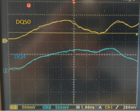
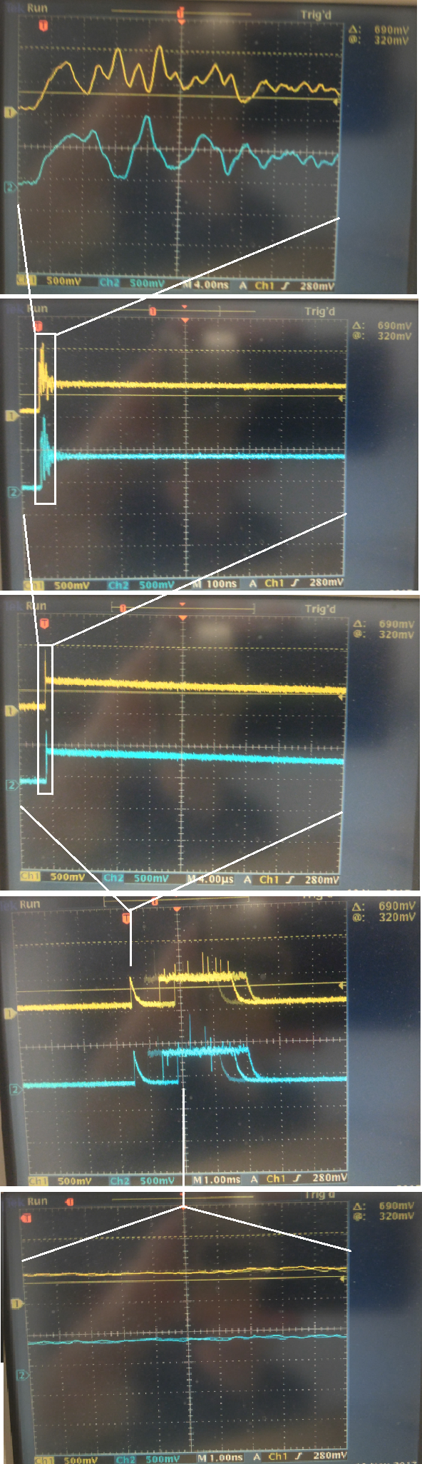
I'm working on a new design using an AM5716 and a single 4Gb DDR3L part #AS4C256M16D3LC-12BCN.  The data is not correct when viewing in the memory browser and I see traces on the data lines that looks incorrect.  While I am sure the SI of this design is not ideal, I think there may be something much bigger that I am still missing.  Perhaps you can spot it!

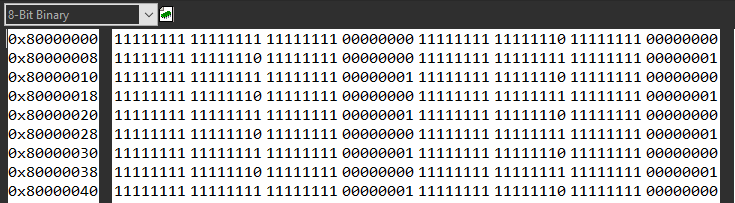
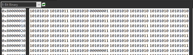
The write errors follow somewhat of a pattern.  I also get more or less sporadic read errors when viewing it real time during continuous reads.

Fill with 0x00000000

Fill with 0xFFFFFFFF

Fill with 0xAAAAAAAA

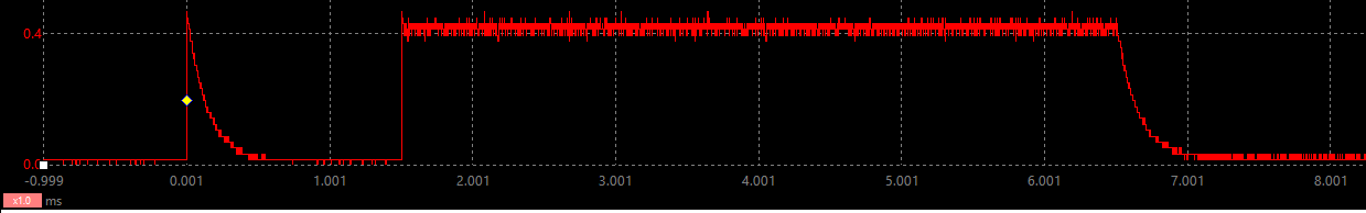
One of the biggest red flags that I might have found is that the data lines seem to not be pulled or terminated at all, perhaps.  The rising edge is quick, but the falling edge is very slow over milliseconds.

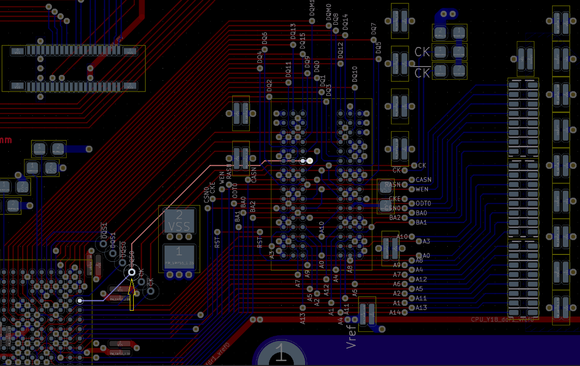
The schematic is shown below:

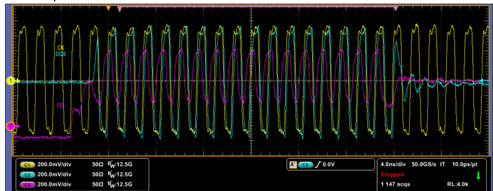
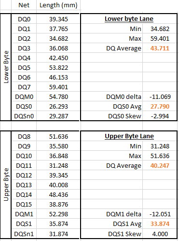
I've attached the EMIF spreadsheet, as well as my custom GEL files.  I am operating the DDR at 400MHz.  I can get other traces or any other information that might be useful. Thank-you for your help!

5381.Attachments.zip

  • Hi Jason,

    A couple of thoughts / questions.

    CL and CWL in the worksheet "Step3-DDRTimings" appear to be set higher than needed. Not sure this is your issue, but would recommend reducing these. Based on the DRAM datasheet, you should be able to use these values: CL = 6, CWL = 5. Please spot check, but this should impact the following parameters in your GEL:

    • SDRAM_CONFIG
    • EMIF_PHY_READ_LATENCY

    I have not yet gone through your GEL files in enough detail, but did notice on line 351 of "Dxo_DDR.gel" the second input parameter to "Dxo_DDR_EmifConfig" is blank. I am not sure what that defaults to when left empty; however, you should set that to 1.

    Please let us know any update based on above changes.

    Thanks,
    Kevin

  • Hi Kevin,

    I've corrected the CL and CWL as you pointed out in the spreadsheet.  It makes sense that the CAS Latency (CL) is adjusted for the frequency (400MHz in my case) to meet the 13.75 nS Taa min spec.  Clearly the setting I had was over the max value of 20nS.  I'm still a bit unclear on what spec in the datasheet drives the CWL latency and was struggling with that earlier - but it does elude to the number you suggested in the Tck(avg) setting for 2.5nS / 400 MHz.  SDRAM_CONFIG and EMIF_PHY_READ_LATENCY are updated in the GEL file now.

    I've also corrected the mistake in my Dxo_DDR.gel file to run hardware leveling (thank-you for catching that!).  It was defaulting to zero, and seems to be running now.

    I have tested and get the same results (both in read/write errors and the odd-to-me trace on the data lines).

    I appreciate the time you've taken in reviewing my design and application files!  I also understand how difficult it is to debug something through the internet.  Please let me know what else I can test or traces to acquire that might help.  You likely don't realize how thankful I am to have some help with this challenging endeavor!

    Updated files are attached.

    Thanks again,
    -Jason

    5545.Attachments.zip

  • Hi Jason,

    Ok, thanks for the update, and all of the detailed info.

    A few high level questions:

    • Is this behavior occurring on more than one board, or has only one board been tested? 
    • If you haven't already, can you verify the voltage rails are correct? At minimal, would suggest confirming the 1.35V rail and VREF. Would also be good to confirm the CPU / CORE rails of the AM5716. 

    A few more debug suggestions:

    • From the memory browser window, there is a continuous refresh button (has yellow arrows, and should say "continuous refresh" when you mouse over it). Can you click this button and see if the memory contents change in the browser window? 
    • Not sure it will tell us much at this point, but can you also try to program different values at each address? Maybe start with 0 and increment by 1 each address. It would probably be easiest to do this through a GEL script or simple c code running from internal memory.
    • In terms of scope captures,
      • We probably need a much smaller time scale (maybe 10ns / div) to be able to understand the waveforms better. You will want a fast sample rate to be able to capture the rising / falling transitions.
      • I am not sure what the voltage scale is, is "0.4" = 400 mV? We should see a high voltage > 675 mV if driving (or reading) a 1. This may also be an artifact of the sample rate if set too slow. Can you confirm that we see > 675 mV when writing all F's (your 2nd fill scenario from previous post)? 
      • As this seems to be gross error across the DDR bus, I would probably recommend to look at common signals before individual data signals (if you haven't already). Ensuring clock looks good and is at the expected frequency is a good first step. Assuming the clock looks good, I would suggest looking at the DQS signals next. If you turn on the "continuous refresh" button from the memory browser window, you should hopefully see the DQS being driven by the DRAM as the controller should be issuing read commands to the DRAM. (This would also give us some confidence that the command signals are most likely working properly) The DQS signal should also show activity when you issue a write in the memory browser window.

    Best regards,
    Kevin

  • Hi Kevin,

    I'll be able to give you a complete response with much faster scope traces in a day or two.   In the meantime...

    Only one board has been fabricated and tested.  Certainly it is possible that a connection is not made properly.  As we exhaust the obvious things, I will work on getting another one built to see if it responds differently.  I have done quite a bit of point to point testing and have not found any shorts so far.

    The voltage rails of the SoC (from a TPS659162) look reasonable, including the 1.35V from SMPS5, and VTT & Vref from the TPS51200.  I did see some noise at 1MHz from an upstream buck converter that I think could be improved.  I'll get some better traces of that and report back.

    I do get read errors sporadically.  With a full screen of data in view there are several read errors per scan.  Writing data to one address can change other addresses directly adjacent (rather predictably).  The (write error?) patterns that you see in the original post are quite consistent.  There are a lot of problems, but they do seem to follow *some* kind of underlying pattern.

    I'll get back to you after doing some more testing.

    Thank-you!
    -Jason

  • Scope Traces!

    Note - I powered the system via a bench supply to set aside any previous noise concerns I had in the upstream power design.

    Clock:

    DQS Signals (ewww):

    A Data line during read / write / and over an extended period of time.

    The view over an extended time looked concerning to me before but perhaps this is normal between commands?  Maybe there is no termination on either side during that time.

    One of the address lines:

    Perhaps this is all just "pretty bad" for a first try at high speed layout. :)  I'm interested to hear your recommendations on next steps and maybe if there is time a chance to review by board design.  Since this might certainly be relevant, the termination resistors are a 43 Ohm array (CAT16-430J8LF - not the 49.9Ohm I show in the schematic).  If by chance my trace layout is not horrible, this can be swapped out easily before resorting to spinning a new board.  Perhaps I should be experimenting with different drive strengths and termination resistances.  As you can see I could use (and appreciate) your advice.

    Thank-you!
    -Jason

  • Hi Jason,

    Thanks for the additional info. The DQS signals look concerning. I may have missed it but I couldn't find the sample rate in the waveforms. I suspect there may still be some under sampling occurring in the DQS and DQ waveforms. How does the DQS signal appear if you match the scope settings used for clock? Also, where are your probe points located (ex: mid-flight, underneath DRAM, etc.)?

    In terms of next steps, we probably need to better understand what is happening with the DQS signal. I'd suggest first trying to recapture the waveform with the scope settings (and same probe) used for clock. If you haven't already, you may also try running IBIS simulations with your board to see how the signal integrity compares to scope measurements.

    Also, a bit of a shot in the dark, but can you try setting the EMIF_PHY_INVERT_CLKOUT to 0x0 (line 600 of your "Dxo_DDR.gel" file)?

    Thanks,
    Kevin

  • Hi Kevin,

    A closer look at the DQS0 signal, along with a data signal:

    Below is a series of views at larger time scales to provide a broader view, FWIW:

    At very large time scales, you can see that there is an initial spike or some kind of transfer followed by a much longer transfer.  However, at no point during that time does there appear to be any real activity (the last image is back at 1nSec scale, but in the later transfer section).  I've also noticed that the voltage levels all seem low?  Should the DQS and data signals be transitioning across Vref?  All traces that I've shown in the pictures are referenced to common.

    The DQS signal was measure mid flight, at this location:

    I did try to invert the clock, as you mentioned, but got the same or similar results.

    Thank-you again, for your help and time looking into this!
    -Jason

  • Hi Jason,

    Sorry for the tangent, but do you have trace lengths for the DQS0/n signals and all the corresponding DQ bits and DM of byte lane 0? I am guessing blue is the  top layer of the PCB. Is red the bottom layer? Mostly asking as the DQ bits look significantly longer than the DQS signals from visual inspection.

    Thanks,
    Kevin

  • Hi Jason,

    >>Should the DQS and data signals be transitioning across Vref?

    Yes, as a single-ended signal it should transition across VREF. If you use a differential probe for DQS, it should transition around 0V. I am attaching an example WRITE waveform interfacing to a DDR3L memory that I have handy on my hard drive. This is just an example, and was not specifically taken with AM5716. 

    You ideally want a short ground for your probe when taking these high speed measurements.

    >>I did try to invert the clock, as you mentioned, but got the same or similar results.

    Ok, thanks for trying this.

  • Hi Kevin,

    I'll report back on the exact lengths.  Blue is the top layer, and red the bottom.  The lengths are probably as different (bad) as they look - length matching is something I overlooked and will need to get right on the next rev.

    Thank-you for the example trace you posted, that is very helpful.

    It looks like the DQS and DQ signals that I see are nowhere near where they should be, and my larger concern is that it can't be explained by improper trace matching...the signals on their own should still be better than what I am seeing.  Something is very suspect about the levels across the board.  If any other thoughts come to mind, let me know.

    Thanks,
    -Jason

  • Hi Jason,

    One quick thought - have you confirmed your resistor connecting pin L8 of the DRAM to ground is 240 Ohm +/- 1% tolerance? (and it has good electrical connection to the L8 pin and ground)? Your schematic shows 240 Ohms, but just asking in case the wrong component was accidentally soldered to the board.

    I agree that the difference in trace lengths wouldn't explain the DQS scope measurements. My original thought was that we might be able to manipulate register settings to try and show some functionality (maybe at a further reduced frequency if we think the SI issues are not due to bandwidth limitations of scope / probe).

    Thanks,
    Kevin

  • Hi Kevin,

    I re-checked that resistor and it looks good (measures 239.9 Ohm), with good continuity to ground.  I am capable of almost any mistake - so I appreciate you asking.

    I created a summary of all the trace lengths.  I am overjoyed at the prospect of adjusting and de-rating with register settings to compensate for this layout.  I am also making notes for changes and goals on the next rev.  Any notes you have for me are more than appreciated.

    The summary for DQS to byte lane mismatch is below.  The full spreadsheet is attached.

    Thank-you!
    -Jason

    DDR Trace Lengths.xlsx

  • I took a few more measurements today, and attempted to capture the *differential* DQS signal like I should have been doing all along.  Using the equipment I have available, I used two probes and the math channel.  I'm happy to report that it looks slightly less horrible than it did before - certainly getting good traces is very much part of the fun here.

    DQS:  I think tPRE is even visible in the first full clock cycle...

    An attempt at getting another trace of a data line.  Still not great - but that could be real or poor measurements.

    -Jason

  • Hi Kevin,

    Regarding your comment -  My original thought was that we might be able to manipulate register settings to try and show some functionality (maybe at a further reduced frequency if we think the SI issues are not due to bandwidth limitations of scope / probe).

    I wonder if you might still have a chance to advise on register settings that might affect timing based on the trace lengths?  I do appreciate that A) this layout may not be feasible, and B) that this might have to wait until you can get to it.  - No worries on all accounts.  However, if 'A' is true, I would greatly appreciate any comments on what to focus on first when re-designing the trace layout.

    I am still very much looking forward to the possibility that I might get this to work (somewhat)!

    Thank-you,
    -Jason

  • Hi Jason,

    I apologize that I never followed-up here. From a spot check, it looked like there may have been too much variance across the byte lanes, and this SOC does not have per-bit deskew. However, if you wanted to check timing relationships between signals you could modulate following parameters:

    Parameter(s):

    • PHY_REG_RD_DQS_SLAVE_RATIO* - Delay between DQ and DQS for reads (this occurs inside the SOC, so not visible with scope). Typical value is 0x40 (or 1/4th clock cycle) to center the DQ on the DQS edge.
    • PHY_REG_WR_DQS_SLAVE_RATIO* - Delay between DQS and clock for writes. When set correctly, signals should be edge aligned at memory.
    • REG_PHY_DQ_OFFSET* - Delay between DQ and DQS for writes. Typical value is 0x40 (or 1/4th clock cycle) to center the DQ on the DQS edge.

    Since it looks like you have a new thread at link below, I am going to close this thread. 

    AM5716: DDR Interface Debug - Proper board routing edition!

  • Hi Kevin,

    Thank-you for getting back to me.  I was interested to hear which parameters can be adjusted to compensate for skew in the signals.  You've been very helpful!  The entire discussion was "the solution" but your last one is marked as such now.

    When you say there was too much variance across the byte lanes, I assume that is referring to DRS35: DBn skew < 5pS, so I'll be sure to get that within spec as I work on the redesign.

    Much appreciated!
    -Jason