This thread has been locked.

If you have a related question, please click the "Ask a related question" button in the top right corner. The newly created question will be automatically linked to this question.

Problem facing with DDR2 interface of DM6446

Normal 0 false false false EN-US X-NONE X-NONE MicrosoftInternetExplorer4

Hello,

We are facing issue with DDR2 interface, till when silicon changed from "TMS320DM6446ZWT" to "TMS320DM6446AZWT".

Below are our observations for DDR2 issue,

-          Tested DDR2 with CCS utility, which will test full DDR address range.

-          Write known data pattern (AAAA or 5555) to full address range and read back for verification.

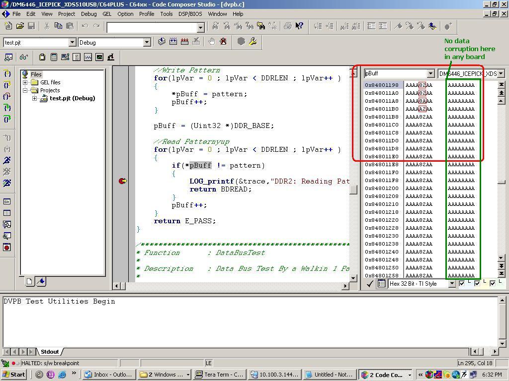
-          Observed that (find attached jpg),

o   Data gets corrupted starting from 0x84801198 address onwards (address changed after each power up).

o   Data is corrupted only for odd / even address (for e.g. in attached image all odd address (highlighted with red color boxes) 0x84801199, 0x848011A1, 0x848011A9, 0x848011B1. )

o   Between the two corrupted data there is 8 address byte offset (which is fix all the time)

o   There is no corruption as shown in green color box (in any board)

o   Add significance delay between two write operation, but still the same.

o   When we write known data to any particular corrupted address (directly in memory window), we are able to successfully write/read.

-          Terminate ODT pin of DDR2 chips to GND, but still the same.

There is no DDR issue in 20% of total build of boards of this batch.

Please advice.

Thanks in advance.


--

Thanks & Regards,

Ashvin Dedakiya

Skype: ashvindedakiya

  • Here are some questions/comments:

    * Does the value printed by the printf statement match what you see in the memory window always?

    * What is the data type of the pBuff variable?

    * Try changing the Access Size for the DDR region in Options->Memory Map and refreshing the memory.

    * If you slow down the interface and relax the timings does it improve? We can use this information to determine if it is a read or write error. Since the CCS memory window reads back correctly when data is written through there, it would appear that the CPU writes are the ones messing up.

    Jeff

  • Jeff,

    Thanks for your inputs.

    -  Yes, printf statement match with memory window always.

    - pBuff is unsigned int.

    - We changed Access size for the DDR region and observed that, it never fail between (0x80000000 to 0x83FFFFFF, 64MB), but always fail near 0x8400xxxx (failed location is not always the same, but region is same).

    - Slow down the interface from 165MHz to 135MHz and up to 100MHz, but still the same.

    Normal 0 false false false EN-US X-NONE X-NONE

    - memfill32() function pass to write(0xFFFFFFFF, 0xAAAAAAAA, 0x55555555, 0x00000000) always (it verify for 1MB locations only).

     - We placed pointer inside code to the corrupted memory and try writing values one by one (not in loop) for failed location, and it passed.

    Normal 0 false false false EN-US X-NONE X-NONE


    --

    Thanks & Regards,

    Ashvin Dedakiya

  • At this point it might be best to check out your layout. Have you verified that it meets all the rules in the datasheet for the DDR layout?

    Jeff

  • dear Jeff,

                   I was puzzled six months by as the same problem, your FAE gave the same advice as you, so I relayouted my PCB and strictly abided TI layout guidance, and I sent my PCB file to your FAE in SHENZHEN to check it, after he checked my PCB layout, I made 10PCS mainboard, but it didn't solve this problem. My PCB layout was layouted by  professional high-speed PCB company, this time is already the second version by  professional high-speed PCB company, so I think this problem wasn't caused by PCB layout.

                  When my DDR2 is K4T1G164QQ-HCF7(DDR-800), if CLK and #CLK are parallel terminating 25pF capacitance to GND respectively, K4T1G164QQ-HCF7 DDR2 on my board can normally work, but K4T1G164QF-BCF7 still doesn't work;

                  when series terminating resistances of CLK and #CLK are replaced with longth 50cm #28 wires, K4T1G164QF-BCF7 can work.  But I don't understand why, can you give me advice for it. How can I solve this problem?

                 Recently, I read JEST79-2F on page 35, it has describe as:'Note that when differential data strobe mode is disabled via the EMR, the complementary pin, #DQS, must be tied externally to VSS through a 20 Ω to 10 kΩ resistor to insure proper operation.  ' Is there problem of the schematic circuit diagram from TI? I studied  MT47H6416BT datasheet,  'DQS is used in a single-ended mode and the DQS# ball is disabled. When disabled, DQS# should be left floating; however, it may be tied to ground via a 20Ω to 10kΩ resistor. ' ;  But  K4T1G164QF and K4T1G164QQ and H5PS1G63EFR-S6C etc. datasheet is that 'Note that when differential data strobe mode is disabled via the EMRS, the complementary pin, DQS, must be tied externally to VSS through a 20 Ω to 10 kΩ resistor to insure proper operation.'

               Pealese  all who met this problem give your debug result. Thanks!

    By Wangxdan

  • Hi By, that indeed is a discrepancy in the TI guidelines and the DDR datasheet. If possible I would advise you to modify the board to put the pull downs, but we don't believe this is the root cause of your issue.

    Most likely it is a software configuration issue. Have you attempted to relax the timings or even slow down the DDR clock to see if there is any improvement?

    We will be reviewing your layout again just to verify everything looks right again.

    Jeff

  • Hi,

    We understand that the near by FAE has inspected your layout. Can you share it with us so that we can take another look at it? Just wanted to be sure.

    Thanks.

    Best regards, Zegeye

  • Dear Jeff,

                    We have already tried to relax the timings and even slowed down the DDR clock at 47MHz , When we met this problem, but it didn't have any improvement.  I don't modify my board to put #DQS pull downs to made mainboard, because I don't have enough proof.    

                    Do you know how Ashvin Dedakiya solved this problem?

    regards&thanks!

    Wangxdan

  • Dear Zegeye,

                           I am pleasured for you attached importance to my problem. I will send my two PCB files to you.  The first PCB file as below:

    5102.Xface_DM6446_MB_SV4_PV5.0_20110623w.rar

                            The second PCB file and sechmatic circuit were checked by TI FAE of ShenZhen as below:

    0284.d__project_xface_dm6446_sch_.pdf  and

    8206.Xface_DM6446_MB_SV4_PV5.0_pcb_blz.rar.

    regards&thanks!

    Wangxdan


  • By the way, my PCB file is layouted by PADS2007.

    Wangxdan

  • Hello Wangxdan,

    After thorough testing, found out that my DDR chips are bad.

    I am able to write data into that, but when read back the same data for verification, it fails. So I am sure processor sending correct data, but it will be not write / read in DDR chips. I have replaced my DDR2 chips, and its working.

    Thanks & Regards,

    Ashvin Dedakiya

  • Hi Ashvin,

    Thanks for your input and taking your time to share your thoughts. We appreciate that very much.

    Did you use another vendor memory or you just replaced with the same kind? Since Wangxdan has redone his h/w, he probably is not using the same memory unless he has a connector (slot)  that accepts memory cards.

    Hi Wangxdan,

    Thank you for your files. We will inspect that and let you know. As I mentioned previously, this is a proven device and Ashvin's comment supports that fact.

    Best regards, Zegeye

  • Dear Ashvin Dedakiya,

                                             Thank you give me replay, you are lucky, because the problem that you met is little trouble. I had tried more ways to slove my problem, for example, using Macron's DDR2 and Hynix' DDR2, but they all failed. I made three times PCBA, the first I doubted that my layout was wrong, so the second I pealsed professional High-speed PCB company to layout, but the problem still didn't solve; they help us to connect TI FAE of Shenzhen, I sent PCB file to TI FAE, He thought their layout didn't strictly accord with TI guide; So We relayouted PCB strictly with TI guide, and we sent  PCB file to TI FAE of Shenzhen to check, after he thought it is OK, I again made PCB, but  the problem didn't be solved. I still am in troble, I am helpless.

    Regards&thanks!

    Wangxdan

  • Dear Zegeye,

                          I used new DDR2 device K4T1G164QF evey PCBA, they all shouldn't be bad, and then they can work when the series terminating resistances of CLK and #CLK are replaced with longth 50cm #28 wires. This phenomenon seemed PCB layout problem, but we didn't solve it by modifing PCB layout, Some High-Speed PCB exports didn't explain my problem, because they had alrerady SI PCB with BISI module, they thought some timing is normal. So we had to doubt my DDR2 sechmatic circuit. But I didn't known where is the error. Because K4T1G164QQ has already been end of life, I must solve this problem in my product. So I am in trouble, I expect you to coach me.

    regards&thanks!

    Wangxdan  

  • sorry, BISI is clerical error,it should be IBS module of device.

  • Dear Zegeye,

                             Do you think my pcb layout is OK? How do I solve my problem? I expect you to coach me.

    Best regards,

    Wangxdan


  • Hi,

    Sorry for the delay. I have pinged the DDR expert for his response. If I do not get somekind of a reply from him, will have to ping him again.

    Best regards, Zegeye

  • Hi,

    The layout file you have posted on 9/25 has been reviewd by a DDR guy and it looks like you are using a power plane as a reference plane. It also appears to have illegal terminators on the CK net.

    You will need to get your layout fixed.

    Best regards, Zegeye

  • Dear Zegye,

                         I don't think your answer can solve this problem.

                        Maybe your FAE not carefully check my PCB file, the PCB file that I gave out is 6 layers PCB by professional high-speed PCB company, the  POWER layer of PCB is on fifth layer, but this layout plane of DDR2 section is layouted as Ground plane, +1.8V plane is third layer in the DDR2 section, So I think reference plane should be right.

                        And that primely, the PCB file by myself layouted was 8 layers, the reference plane had 3 reference Ground plane,  these PCB had the same problem, and because  these 8 layer PCB had this problem, we decided to seek help of the professional high-speed PCB company layouting my PCB.

                       Which one is the  'illegal terminators on the CK net'?  Are the CLK and #CLK parallel terminating 25pF capacitance to GND respectively? They were appended for K4T1G164QQ DDR2 . I had already explained in frontal intercommunion; if I don't appended them, K4T1G164QQ DDR2 also had the same problem.

                       Are the CLK and #CLK serial terminating 47 ohm resistance respectively? They already have existed in the design of TI, and I tried to replace them with from 0 ohm to 200 ohm, even more kinds different resistance, but furitless.

                       So I hope you to give me else advices, I am alreagy helpless, how do I modify my PCB or sechmatic circuit to slove this  fatal problem?  Or how I modify software configuration files? I had layouted the fifth PCB file, but I still don't know how can I solve my problem? Can you give me a new hope? Urgent Urgent!!!

    Best Regards

    Wangxdan

  • Hi,

    Just want to make sure. Since I started looking into your case recently, I would like to know if you have sent a layout file prior to 9/25 or is that the only one you sent us? I want to make sure that the right layout file was reviewed. It seems that there is no coorelation between your current response the review I posted today.

    Best regards, Zegeye

  • Dear Zegeye,

                           I sent two PCB files to you in 9/25,  they all  are 6 layers, the file 8206.Xface_DM6446_MB_SV4_PV5.0_pcb_blz.rar is latest layout, it was checked by FAE of TI SheneZhen office. Two PCB should be right, because the latest PCB layout is only nearer TI layout guidance than  prior PCB file, and  according as debugging instance, CLK and #CLK are parallel terminating 25pF capacitance to GND respectively for suring K4T1G164QQ normal. But K4T1G164QQ is end of life, new else DDR2  have problem. You can only check latest PCB.

    Regards&Thanks!

    Wangxdan


  • Hi Wang,

    Could you please advise who checked your PCB in TI Shenzhen office? Could you please advise the name? We shall follow up accordingly.

    Thanks,

    Cui Jing

  • Dear Cui,

                  Sorry,  What I need only is that my problem can be solved, I thought everyone who gave me some advices is a good man, because he exerted himself to help me. What I need is that TI's engineer  help me to seek out my mistake of my PCB or schematic circuit or software config etc. After all this is a forum that engineers discuss question, so please don't ask me about  things are disrelated with technology. If you have a good advice about it, pealse speak out it, I will try to do it, after seriously considering.  You don't worry me to blame you. Thank you!

    Regards!

    Wangxdan

  • Dear Zegeye,

                          Can you give me a new progress? I hope my problem can be solved on my new project. Think you!

    Best regards!

    Wangxdan

  • Hi Wang,

    I understand your situation. Sorry, I did not give you more background information. Zegeye is on travel now. We want to contact you over phone or mail since that might be more efficient. That is why I asked you that question. Then, I would to have the FAE contact you again. Our FAE can work with Zegeye together to help you. After internal check, we are not sure which FAE has supported you. Could you please advise the approch you prefer that should be used to support you?

    Thanks,

    Cui

  • Dear Cui,

                   Sorry, maybe I mistaked  that you would blame the FAE who he ever coached me in Shenzhen, so I refused your demand, I shouldn't bring him in trouble, he already did his possible to help me. I thanked him very much.

                   Of course, now I understood your meaning. I will be pleased with your help, Tuff Li ever coached me on this problem, but this problem really is difficult for him and me, so I had to appeal on the forum. My phone is 0755-26738111-8020, my E-mail is wan.xd@163.com and wxd@xfacetech.com.

    Best Regards!

    Wangxdan

  • Hi Cui,

                Recently, Tong from Shenzhen TI Office had helped me to look for reason of my problem, but he was no way. He asked me to replace DM6446 with DM6443 from him, and replaced K4T1G164QF-BCF7(6-6-6 800MHz) with K4T1G164QF-BCE6(5-5-5 667MHz), but these didn't slove my problem. So I thought the problem didn't come from chips quality; Tong should be good at software,  so I couldn't doubt soft configuration again, as DDR2 timing really is error; lastly I had to doubt PCB layout and schematic ciucuit, but our PCB layout designer was from professional high speed PCB company, and then DDR2 section of schematic circuit was the same as sechmatic of TI EVM completely. But it don't satisfy a demand from DDR2 datasheet, this demand is below:

             " In differential mode, these timing relationships are measured relative to the crosspoint of DQS and its complement, #DQS. This distinction in timing methods is guaranteed by design and characterization. Note that when differential data strobe mode is disabled via the EMRS, the complementary pin, #DQS, must be tied externally to VSS through a 20 Ω to 10 kΩ resistor to insure proper operation. "

                Whether can you help me to seek that a DDR2 expert will check this point and my PCB? DM6446 isn't in differential mode, but #DQS is float, it don't be tied externlly to VSS though a resistor. I was in trouble for eight months...

    regards&thinks!

    Wangxdan


  •  Hi Xdan,

    We will review the layout again.

    Thanks,

    Jing

  • Dear Jing,

                       Happy new year! Do you remember my problem? Please review my layout and schematic circuit of DDR2 part, I wait your guidance for my product.

    Regards&Thanks!

    Wangxdan

  • Hi Wangxdan,

    Happy New Year!

    Enclosed is our layout review feedback. There are some violations, please refer to our DDR layout guideline in data sheet and modify accordingly.

    Thanks,

    Cui Jing

    DM6446_review.doc
  • Hi Cui,

                  Thank you very much! I carefully read your review, and seriously studied it. I have given my new doubt, they are blue font in the enclosed file. For “1.1.8 return current bypass capacitors”,I don’t see it, because my DDR2 return current plane all are GND plane (layer 2 GND plane and layer 5 GND plane), reference plane net don’t be changed; how should I connect return current bypass capacitor? Are two terminals of 0.1uF bypass capacitor connected to GND net as below? If  it is, how much do they need?I need you give me more detailed guidance.

    1220.DM6446_review20120109.doc

    Regards & Thanks!

    Wangxdan

  • Hi Wangxdan,

    If all the return current planes are ground planes, you just need return current ground vias sprinkled where you make layer transitions that change the reference planes.

    Thanks,

    Cui Jing