This thread has been locked.

If you have a related question, please click the "Ask a related question" button in the top right corner. The newly created question will be automatically linked to this question.

66AK2G12: QSPI read dummy cycles

Part Number: 66AK2G12

Hi,

I have a question from my customer about QSPI read cycle.

He is trying to read data from QSPI flash, but read data are 1byte shifted as below.
Written data: 0x00000000, 0x12345678
Read data: 0x00000012, 0x34567800

He checked QSPI waveform and wonders dummy cycles are not aligned between Flash and K2G.
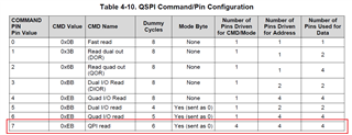
As you can see below waveform, the flash memory send data 8 cycles after address field.
But it seems K2G side takes the 1st read byte 6 cycles after address field.


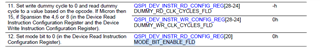
Register configurations are below.
DUMMY_RD_CYCLES_FLD=0x4 and MODE_BIT_ENABLE_FLD=0x1, so total cycles are 4+2=6 cycles.


Then customer changed DUMMY_RD_CYCLES_FLD, but waveform did not change.
Is there any missing configuration to change dummy cycles?

Thanks and regards,
Koichiro Tashiro

  • Tashiro-san

    I'll have to dig into this and get back to you. 

    --Paul 

  • Hi Paul,

    Any progress?
    Could you update the status?

    Thanks and regards,
    Koichiro Tashiro

  • Apologies for the delay. 

    Can you clarify why the values were chosen for MODE_BIT_ENABLE_FLD and MODE_BIT_ENABLE_FLD?

    Looking at the TRM  the Direct Access Controller Programming sequence has the following:

    Thanks

    --Paul

  • Hi Paul,

    Customer selected MODE_BIT_ENABLE_FLD=1 as this configuration is used for BOOTMODE=QSPI96MHz.
    Do you mean DUMMY_RD_CLK_CYCLES_FLD is valid only when MODE_BIT_ENABLE_FLD=0?

    Thanks and regards,
    Koichiro Tashiro

  • Hi Paul,

    Any updates?
    Customer is waiting for your reply.

    Thanks and regards,
    Koichiro Tashiro

  • Hi,

    What other parameter did the customer set when initializing QSPI?

    Some additional QSPI configuration information about dummy cycles/bytes can be found in the TRM in table 4-10, table 4-24, table 11-3223, and table 11-3304.

    One particular piece of information that I found in table 4-24 is that the number of dummy bytes used when the boot mode is 96MHz is 8.

    Best regards,

    Dillon

  • Hi Dillon,

    Please find below feedback from the customer.

    For Table 11-3304
    Address: 0x0294 0090, Value: 0xEBCA 0180

    For Table 11-3223
    Address: 0x0294 0004, Value: 0x0612 2200

    For Table 4-10
    QSPI BOOT MODE: 0x8449
    In current setting, COMMAND PIN is 0x2(CMD Value 0x6B).
    This will be changed to 0x4(CMD Value 0xEB)

    For Table 4-24, customer will check them and let you know.

    Thanks and regards,
    Koichiro Tashiro

  • Hi Dillon,

    Here is Table 4-24 values.

    Byte Offset22: 0x01FE
    Byte Offset24: 0x0018
    Byte Offset26: 0xFFFE
    Byte Offset28: 0x0000
    Byte Offset30: 0x03C0
    Byte Offset32: 0x0000
    Byte Offset34: 0x0000
    Byte Offset36: 0x4080
    Byte Offset38: 0x0108
    Byte Offset40: 0x0F00
    Byte Offset42: 0x00EB
    Byte Offset44: 0x0000
    Byte Offset46: 0x0006
    Byte Offset48: 0xC0C0
    Byte Offset50: 0x2E2E
    Byte Offset52: 0x0000

    Thanks and regards,
    Koichiro Tashiro

  • Hi,

    There is one correction is previous post.

    For Table 4-10
    QSPI BOOT MODE: 0x8449
    In current setting, COMMAND PIN is 0x2(CMD Value 0x6B).
    This will be changed to 0x4(CMD Value 0xEB)

    It was not correct. Correct configuration is COMMAND PIN = 7, so CMD Value = 0xEB.
    The system boots up with QSPI 96MHz, so Dummy Cycles = 6 clocks for QPI read is selected according to Table 4-10.


    After boot-up, customer changed DUMMY_RD_CLK_CYCLES_FLD, but dummy clock cycle did not change.
    4 clock, 6 clock, 8 clock were tried.
    Are there any reasons why dummy clock cycle is stuck to 6?

    Thanks and regards,
    Koichiro Tashiro


  • Hey Koichiro,

    There is no obvious reason why their changes to the dummy cycle value are not taking effect, it could be a software issue with how they access QSPI. Can you verify if they are directly accessing the memory region associated with QSPI, or if they are using the STIG? 

    Sincerely,

    Lucas

  • Hi Lucas,

    Sorry for my late reply.
    I had some discussion with customer and found followings.

    - In fact customer was using STIG(QSPI_FLAH_CMD_CTRL_REG and QSPI_FLAH_CMD_ADDR_REG),
    but what customer really wants to do is direct access to the QSPI memory region(0x2400:0000 to 0x27FF:FFFF).
    I guess this is so-called “XIP mode”, correct?

    - According to TRM, Direct Access Controller(DAC) is used to directly interface to the memory mapped region.
    So customer tried with below settings in QSPI_CONFIG_REG.
    ENTER_XIP_MODE_IMM_FLD=1
    ENTER_XIP_MODE_FLD=0
    ENB_AHB_ADDR_REMAP_FLD=0
    ENB_DIR_ACC_CTLR_FLD=1
    ENB_QSPI_FLD=1
    (You can see full register dump in attachment)
    QSPI_configuration.xlsx
    But it does not seem working.
    When target address (0x2400:0000) is written with data 0x1234:5678, no CMD, ADDR, DATA are generated on QSPI signals.
    (Write access is done via CCS Memory window)

    - Customer also tried with different configuration in QSPI_CONFIG_REG
    ENTER_XIP_MODE_IMM_FLD=0
    ENTER_XIP_MODE_FLD=1
    ENB_AHB_ADDR_REMAP_FLD=1
    ENB_DIR_ACC_CTLR_FLD=1
    ENB_QSPI_FLD=1

    But the result was the same. No CMD, ADDR, DATA are generated on QSPI signals when 0x2400:0000 is accessed via CCS Memory window.

    I checked TRM description, but it is really complex and difficult to understand.
    For example:
    - Is there any difference between using “DAC” and “XIP mode”? It seems both directly access to the memory mapped region(0x2400:0000 to 0x27FF:FFFF).
    - In QSPI_DEV_INSTR_RD_CONFIG_REG.RD_OPCODE_NON_XIP_FLD (TRM Table 11-3223), it says “Read Opcode in non-XIP mode: Read Opcode to use when not in XIP mode.” Does this mean this OPCODE is not used in XIP mode? If so, in which mode the OPCODE is used? What OPCODE is used in XIP mode?
    - It is not clear enough how to configure necessary configuration registers to directly access to the memory mapped region.

    Thanks and regards,
    Koichiro Tashiro

  • Hey Koichiro,

    Just to clarify a couple of things:

    - As an FYI, I've never used this device myself but the controller for the QSPI module looks to be similar (if not the same) as the ones in the more recent devices I've used. Looking over the TRM everything seems to translate almost exactly, but I won't be sure of any device nuances that could be present.

    - The reason why the dummy cycles wouldn't have taken effect in the customer's initial question then is because the dummy cycles used by the STIG is in a separate register (QSPI_FLASH_CMD_CTRL_REG it looks like), modifying that with the updated values should have it take effect.

    - DAC, XIP, XIP mode (I'm gonna break down my understanding of each to provide background info)

    • DAC: Basically means the mode where a bus initiator (the A15 or DMA or other core) sends a write or a read to the SoC memory region associated with QSPI. The address accessed in the flash will be based off the offset from the beginning of the SoC memory region.
    • --------------------------------------------------------------------------------------------------------------------------------------------------------------------------------
    • XIP (eXecute-In-Place) : This basically means that a core is executing it's instructions directly from the flash itself by performing read instructions through the DAC interface, without copying over the instructions to internal RAM or a faster memory like DDR. Normally a bootloader would copy over the information from flash into a faster memory, but depending on device definition or customer constraints this is an option around needing other memory.
    • ---------------------------------------------------------------------------------------------------------------------------------------------------------------------------------
    • XIP mode: This is a mode that the controller supports and most (not all) flash devices support. This will seem confusing, but XIP mode is NOT required to do XIP, it just increases the performance slightly. This refers to placing the controller AND flash in a mode where only reads are done (since XIP is just doing read instructions to the flash), so the controller will not send the read opcode and the memory will not expect the read opcode; Address and Dummy cycles are still expected. This can be cumbersome as the flash and controller need to be in sync, and to perform any other operation (write, erase, register read/writes), a flash will have an exit sequence to exit out of XIP mode.
    • --------------------------------------------------------------------------------------------------------------------------------------------------------------------------------

    - Now as to why reads/writes through the memory browser are not generating any output signals, (assuming they're using the A15) can you have the customer check their MMU configuration to see if the QSPI memory region is marked as cacheable (likely Write-Back Write Allocate)? The MMU controls properties for the memory regions, if it's marked as WBWA then the write will only go to cache and not go to the actual memory endpoint. One step you can do to more easily check this is ask the customer to temporarily disable the cache and re-run their memory browser test.

    - As far as the register configuration, I would turn off all XIP mode bits (it sounds like the customer hasn't enabled XIP mode on their target memory anyways if they're trying to do writes). Again, XIP mode is not required to do XIP, it just provides a small performance increase (2 cycles of the command opcode saved) at the expense of not being able to do any other operation while in XIP mode.

    Hope this helps!

    Sincerely,

    Lucas

  • Hi Lucas,

    Thanks a lot for your detailed explanation!
    Now customer is able to read/write QSPI memory mapped region using DAC (w/ XIP mode bits OFF).

    Thanks and regards,
    Koichiro Tashiro