

Part Number: AM3352
Other Parts Discussed in Thread: AM3358, AM3354, AM3359, , AM3356, AMIC110, SYSCONFIG
Tool/software:
Hi TI Experts,
Can you provide a List of E2Es that can be referred when starting a custom board hardware design?

This thread has been locked.
If you have a related question, please click the "Ask a related question" button in the top right corner. The newly created question will be automatically linked to this question.
Hi Board designers,
The below links are a quick reference to the E2Es and FAQs that can be referred when starting a custom design.
E2E
AM335x - Frequency Speed Grade Identification via Register
https://e2e.ti.com/support/processors-group/processors/f/processors-forum/253383/am335x---frequency-speed-grade-identification-via-register/888534?tisearch=e2e-sitesearch&keymatch=zce%25252520zcz#888534
AM3358: are ZCZ ZCE wafers identical?
https://e2e.ti.com/support/processors-group/processors/f/processors-forum/974406/am3358-are-zcz-zce-wafers-identical
AM3358: Temperature grade identification
https://e2e.ti.com/support/processors-group/processors/f/processors-forum/710934/am3358-temperature-grade-identification
AM3354: Device differences vs AM3358
https://e2e.ti.com/support/processors-group/processors/f/processors-forum/1234194/am3354-device-differences-vs-am3358
AM3359 - ZCE, ZCZ differences
https://e2e.ti.com/support/processors-group/processors/f/processors-forum/306246/am3359/1065929?tisearch=e2e-sitesearch&keymatch=zce%252520zcz#1065929
am335x power sequence
https://e2e.ti.com/support/processors-group/processors/f/processors-forum/375367/am335x-power-sequence/1321777?tisearch=e2e-sitesearch&keymatch=zce%25252520zcz#1321777
How much pressure of heat sink can AM3352 chip stand?
https://e2e.ti.com/support/processors-group/processors/f/processors-forum/262665/how-much-pressure-of-heat-sink-can-am3352-chip-stand/919075?tisearch=e2e-sitesearch&keymatch=zce%252525252520zcz#919075
Minimum Number of Layers for AM335x
https://e2e.ti.com/support/processors-group/processors/f/processors-forum/272916/minimum-number-of-layers-for-am335x/953363?tisearch=e2e-sitesearch&keymatch=zce%25252525252525252520zcz#953363
Differences with lower pin packages?
https://e2e.ti.com/support/processors-group/processors/f/processors-forum/213631/differences-with-lower-pin-packages/754374?tisearch=e2e-sitesearch&keymatch=zce%25252525252525252520zcz#754374
AM35x RGMII interface IO voltage
https://e2e.ti.com/support/processors-group/processors/f/processors-forum/189053/am35x-rgmii-interface-io-voltage/678415?tisearch=e2e-sitesearch&keymatch=zce%252525252520zcz#678415
AM335x MPU clock ZCZ to ZCE configuration
https://e2e.ti.com/support/processors-group/processors/f/processors-forum/517675/am335x-mpu-clock-zcz-to-zce-configuration
[FAQ] AM3352: Number of assigned MAC addresses
e2e.ti.com/.../faq-am3352-number-of-assigned-mac-addresses
How to get started with AM335X for customize board development?
https://e2e.ti.com/support/processors-group/processors/f/processors-forum/385444/how-to-get-started-with-am335x-for-customize-board-development
FAQs

Hi All,
Additional inputs
Customer is asking if there is a way their firmware can tell if the CPU is AM3352 or AM554D80 or Z100? Like a register to read from?
Please refer to the below register
Data sheet reference:
3 Device Comparison
Table 3-1 lists the features supported across different AM335x devices
DEV_FEATURE register value(5)
TRM reference
https://www.ti.com/lit/ug/spruh73q/spruh73q.pdf
Table 9-26. dev_feature
Register Field Descriptions Bit Field Type Reset Description 31-0 dev_feature_bits R 0h Device-dependent, See Device Feature Comparison table in device data manual.
FYI, the below thread could be reference.
(+) [Answered] Predefined Macro for AM335x - Processors forum - Processors - TI E2E support forums
Please refer below summary of inputs i received from the expert and this is in line with the above inputs i provided.
The device_id register will be the same for each device of the same silicon revision. You will not be able to determine a specific GPN using this register, just the device revision
The DEV_FEATURE register is the correct register for GPN identification The Device Feature Comparison table in the datasheet has a register value associated with each GPN.
In addition, the efuse_sma register contains details on the package type and max frequency.
Regards,
Sreenivasa
Hi Board designers,
E2Es related to pullup/pulldown
5.7 DC Electrical Characteristics

GPIO source/sink current specifications and pullup value (in current)
We are using the GPMC_A10 GPIO to drive the LDO enable pin.
AM335x Sitara Processors datasheet (Rev. L)

Controlling LDO Enable using GPIO (GPIO to drive LDO):
The AM335x outputs were not designed to support continuous drive of large steady-state current. They were designed to drive CMOS inputs which only requires a transient current to change the signal logic state and potentially a small steady-state current to hold a logic state by over-driving weak pull resistors.
The datasheet publishes VOH and VOL parameters for the LVCMOS buffer type in the Electrical Characteristics section. These parameters represent the device output voltage for a specific drive current."
Additional inputs:
The AM335x outputs were not designed to support continuous drive of large steady-state current. They were designed to drive CMOS inputs which only requires a transient current to change the signal logic state and potentially a small steady-state current to hold a logic state by over-driving weak pull resistors.
The datasheet publishes VOH and VOL parameters for the LVCMOS buffer type in the Electrical Characteristics section. These parameters represent the device output voltage for a specific drive current. This single data point is all we provide. You would need to use the information provided in the IBIS file to simulation output voltage for any other current.
Regards,
Sreenivasa
Hi Board designers,
E2Es related to MMC
AM3356: Is a pull-up needed on MMCx_CLK ?
e2e.ti.com/.../am3356-is-a-pull-up-needed-on-mmcx_clk
You need to be more specific with which MMCx_CLK signal function is being used and which pin is it multiplexed? However, I can give you a high-level overview of why an external pull-up may be required.
Each MMCx_CLK signal function is pin multiplexed with other signal functions, where the pins associated with these signal functions default to a GPIO signal function in high-impedance state with a weak internal pull-up or pull-down turned on. An external pull-up is needed to hold the input of the attached device in a valid high logic state until software configures the pin mux logic to source the respective MMC clock signal to the attached device. Internal weak pull-ups are not recommended to hold signals in a valid logic state when not driven. The internal resistors are primary implemented to hold unconnected pins in a valid logic state when no PCB trace is connected to the pin. It is easy for noise to couple into undriven signal traces and over-drive the internal pull resistors, so we recommend external pulls to hold valid logic states any time a PCB trace is connected to a pin.
GPIO related important E2Es:
AM3352: Sitara Linux crash issue
It sounds like a marginal timing issue. I suspect they are on the edge of providing proper timing to either the eMMC device or the AM335x device. Did the customer perform a timing analysis during their PCB layout to make sure the PCB signal traces have the proper delays to ensure valid timing for both devices
The eMMC interface on AM3354 is exactly the same as the eMMC interface on AM3352. Therefore, I can only assume their eMMC implementation was marginal all along and some small process variation between their pervious AM3352 devices and their current AM3354 devices is revealing the marginality of their implementation.
Each device has input timing requirements (setup and hold for each data and cmd signal relative to clock). Each device also has output switching characteristics (data and cmd signal delays relative to clock). The output switching characteristics need to be combined with the PCB delays then compared to the attached device input timing requirements to confirm there are no timing violations. If so, it may be necessary to increase or decrease some signal trace lengths relative to the other signal trace lengths to insert appropriate delays that meet the all timing requirements of both devices.
You cannot simply make the signal traces short with equal lengths and assume this is a good solution.
Please refer to the MMC Electrical Data and timing section in the AM335x datasheet for the AM335x MMC timing parameters, and your specific eMMC device datasheet to find its timing parameters.
I did not see anything obvious in the oscilloscope waveforms provided in the last post. However, they do not show a timing relationship of any signal relative to clock. You should be using the oscilloscope to measure setup and hold provided to each device and make sure this PCB design is not violating any of the device input requirements. When capturing data transitions, it is difficult to know if you are capturing data driven by AM335x or the eMMC device. I typically capture data over a long period of time with persistence turned on. This will allow you to see data driven from both devices, where you see two transition points for data relative to clock. The one that occurs first is typically data driven by AM335x and the second is data driven by the eMMC device. The is the case since the eMMC device data is delayed more because the clock must propagate across the PCB from AM335x into the eMMC device with some additional delay inserted by the eMMC device.
Pull-up/pull-down resistors are only need to hold input buffers in a valid logic state when not being driven by either device. Adding these resistors after the fact with wires is more likely to cause problems that resolve them, due to their effect on signal integrity. However, there can be long term reliability concerns for the device if you allow inputs to float to mid-supply.
The eMMC specification requires all eMMC devices to turn on internal pull-up resistors on the DAT[7:1] pins. These internal pins get turned off once the device is told they are being used for data transfers. After the bus width changes, the eMMC device turns its internal resistors off and the host is expected to turn its internal resistors on any time it is not driving the signals. This assumes the host supports this capability. If not, external resistors are expected on the signals to hold them in know states. You should refer to the schematic checklist to see if external pulls are recommended for AM335x.
e2e.ti.com/.../5172479
AM335x sends the SPI clock out of the device package pin and loops it back into the SPI controller from the same pin to help with timing closure of the peripheral. This can be problematic when you do not insert a series termination resistor near the AM335x SPI clock pin. The non-monotonic transition at mid-supply is creating glitches on the looped back clock inside the AM335 device and over-clocking the SPI controller. You must insert a 22 - 50 ohms series termination resistor near the AM335x SPI clock pin so this signal distortion is shift up on rising edges and down of falling edges, such that the non-monotoic event is not near the switching threshold of the AM335x SPI clock input buffer. Your branching of the clock into to paths is not helping matters. The non-monotonic event is most likely caused by reflections from one or both branches in the clock path.
The series termination resistor requirement is defined in the in the Peripheral Clocking section of the AM335x Schematic Checklist.
You may need to perform signal integrity analysis on the branched clock path and change your PCB layout to minimize reflections on this signal. For example, you may need to implement a very short balanced-T topology PCB trace for the clock to prevent this from happening.
e2e.ti.com/.../3855179
The datasheet indicates this pin will have a internal pull-down turned on during and after reset. It is not actively driven low. The internal pull-down only sinks about 100uA, so it would not take much to pull this pin high. What is connected to this pin? Is it possible the external components connected to this pin have internal pull-ups that are strong enough to over-drive the AMIC110 pull-down?
You need to check your design to make sure external components are not in conflict with internal pulls of AMIC110, so they do not create a mid-supply voltage on the AMIC110 pins. The AMIC110 input buffers are turned on by default and applying a mid-supply voltage to the input buffer will create shoot-through current that could damage the input buffer if this condition is left for too long.
e2e.ti.com/.../3654906
Are you asking for input impedance looking into one of the AIN pins of the ADC? If so, that is defined in the datasheet.
Input impedance of AIN[7:0], when ƒ = frequency of applied signal: [1 / ((65.97 × 10E–12) × ƒ)] Ω.
This defines the dynamic input impedance.
The input could also have about 1uA of leakage current as the applied voltage approaches VDDA_ADC or VSS_ADC, where the AIN pin sources current when the voltage applied is less than mid-supply and the AIN pin sinks current when the voltage applied is greater than mid-supply.
e2e.ti.com/.../3724253
AM335x has many subsystems which could contribute to power consumption. You need to review your DS0 configuration of all subsystems as well as your DS0 configuration of all IOs.
Reviewing the configuration of each IO relative to external connectivity is commonly over looked as a contribution to power consumption. It is important to configure all IOs so they do not consume power. I will describe a couple of examples where your IO configuration may contribute to power consumption. AM335x will consume additional current if an internal pull-up resistor is being pulled down by an external component. AM335x will also consume additional current if a mid-supply voltage is applied to a pin when the respective input buffer is enabled. This can happen when a signal has conflicting pull resistors. This mid-supply condition should be avoided as it can also create a device reliability issue. This condition cases shoot-through current to flow from VDD to VSS via the input buffer and the device was not designed to sustain this condition for long periods of time.
e2e.ti.com/.../3851264
What you observe on this signal depends on where you connected the probe, the bandwidth of your probe/scope, and quality of your scope probe ground.
You will need a very high bandwidth probe and scope to observe short over-shoot, under-shoot, and non-monotonic events on the signal. I recommend using a low capacitance FET probe with a very-very short low loop inductance ground.
You will see a mid-supply step on the signal when probing near the source. This occurs because the output impedance of the MMC0_CLK output buffer, series termination resistor, and characteristic impedance of the PCB signal trace creates a voltage divider. The voltage divider output is applied to the source end of the PCB signal trace. This voltage propagates down the trace to the far end where it encounters a high impedance load which causes a in-phase reflection that returns to the source. Therefore, the voltage transition observed on the far end will be a continuous transition between VSS and VDD. The is not the case for the source end, as it steps to a mid-supply determined by the voltage divider values and the transition only continues to VDD or VSS once the reflection returns from the far end. You need to select a series resistor value that allows the MMC0_CLK pin to step through the voltage of (VDDSHV4 / 2) without pause. I suggest the step observed on the MMC0_CLK pin should be at least 200mv above (VDDSHV4 / 2) on the rising edge and at least 200mv below (VDDSHV4 / 2) on the falling edge.
e2e.ti.com/.../4183884
I do not think the voltage change observed on the clock signal while it is high is causing your problem. It appears you are probing the clock signal near the eMMC device based on the shape of the clock signal rise/fall edges. You need to probe the clock signal near the processor. I suspect you will see a non-monotonic transition near mid-supply on the source end of the PCB trace. This non-monotonic transition is likely causing the problem.
The processor sources the clock out to the eMMC device and loops in back at the processor pin to improve timing margin. So there is a good chance the non-monotonic transition occurring at the source is creating a glitch on the clock that is looped back into the processor.
The AM335x schematic checklist tells you to install a 33 Ω series resistor on MMCx_CLK (as close to the processor as possible). I do not see this resistor in your schematic. This resistor is necessary to prevent this problem.
The capacitor is likely changing the signal distortion enough to make it work better, but it is not a good solution.
The resistor doesn't eliminate the non-monotonic transition. It shifts the voltage away from the input buffer switching threshold voltage, where it is less likely to create a glitch on the looped back clock going back into the processor. The only way to resolve the clock glitch issue is install a 33 ohm series termination resistor located very close to the AM335x pin. The trace length between the processor pin and the series resistor should be as short as possible.
e2e.ti.com/.../1245193
This input has a weak pull-up enabled after reset is released, but is high-impedance while reset is applied. The internal pull-up should be able to hold the input high if you do not connect any signal trace to the EXTINTn terminal. However, this topology may allow the input to float to a mid-supply level while reset is applied and this may cause a slight increase in power consumption on the VDDSHV6 power rail during this period.
Connecting an external pull-up may not be necessary for your application, but is the best way to insure you do not have any issue with this terminal floating during reset.
Regards,
Sreenivasa
Hi Board designers,
Refer below FAQ related to AM335x clock:
OSC0 input is powered from the VDDS_OSC power rail, which is 1.8V. Absolute maximum input voltage for this input is VDDS_OSC +0.3V. Absolute minimum is -0.5V. It's important to note that no external voltage should be applied to OSC0 pin before the VDDS_OSC supply has fully ramped-up and stabilized. This means that you should either use an external oscillator powered from VDDS_OSC, or place an external 1.8V buffer powered from VDDS_OSC.
(19) AM3358-EP: Overdriving oscillator input - Processors forum - Processors - TI E2E support forums
(19) AM3358: OSC0 crystal requirements - Processors forum - Processors - TI E2E support forums
(19) AM3358: Frequency accuracy - Processors forum - Processors - TI E2E support forums
Crystals are defined to have an initial frequency accuracy at room temperature. They should also provide another parameter that defines frequency deviation due to temperature change relative to room temperature. They typically provide another parameter that defines a frequency change due to aging.
You must combine all three contributors of frequency error to determine the maximum frequency deviation expected across operating conditions for the life of the product.
I have included a couple of links to crystal datasheets that you can use as examples.
ABM11W-25.0000MHZ-8-D1X-T3: https://abracon.com/Resonators/ABM11W.pdf
ABM10W-25.0000MHZ-8-D1X-T3: https://abracon.com/Resonators/ABM10W.pdf
Keep in mind the crystal doesn't dissipate much power, so there is no significant self-heating. The operating temperature of the crystal is typically the same temperature as the PCB board. Therefore, a crystal rated for 85 degrees Celsius may be good enough for most applications.
(19) AM3358: Am3358 - Processors forum - Processors - TI E2E support forums
The RTC logic in AM335x does not play any role in the various low-power sleep states support by AM335x while power remains on. These low-power sleep states are defined by software, where clocks are stopped for some logic functions and clock frequency reduced for other logic functions. You need to research the various modes supported by your operating system.
The Power Estimator Tool is the best way to understand current consumption based on your specific use case.
The RTC drift will be a function of the crystal circuit you connect to the RTC oscillator. In a typical application the RTC is constantly updated by the processor operating system while it has power, which gets its time from a accurate on-line time source. The RTC only needs to keep time while the processor is turned off. The off-time is typically short relative the time it takes for the drift to be a concern. The RTC will be updated by the operating system again after it turns on the PMIC, the processor boots the operating system, and it gets access to an accurate on-line time source.
Based on your questions, you have not read the TRM or researched what is supported by software. I will not be able to talk you through all of these details. You need to research your options.
The crystal shunt capacitance is in parallel with the series combination of C1 and C2. If the crystal requires a load of 18pf to oscillate at the correct frequency, the formula is saying you subtract the crystal shunt capacitance from the load it expects to determine what external capacitive load needs to be added to reach a load of 18pf. In this case it would be 18pF - 5pf = 13pf. Assuming your PCB traces have zero capacitance, the values for C1 and C2 would need to be 26pf. However, there is a good chance your PCB has 2pf to 3pf of capacitance on each signal trace. You would need to subtract that from the calculated value of 26pf and select a value like 24pf for C1 and C2.
The datasheet limits are for the combination of the external capacitor plus your PCB trace capacitance. Therefore, a crystal that requires 18pf of load would not be a good choice for this device.
I'm not sure why the boards you mentioned were designed to use a crystal that requires a load of 18pf. I suspect the TI board was designed before the oscillator limits were defined and the BeagleBone board simply followed the example and used the same crystal. I would not recommend following their example by selecting a crystal that operates outside of the limits defined by the datasheet.
It is not unusual to find the crystal circuit producing a clipped sinusoid waveform on the oscillator XTALIN. The oscillator will produce a reference clock as long as the signal swing on XTALIN exceeds the Vih min and Vil max values defined in the Electrical Characteristics table of the AM335x datasheet. However, the slow changing sinusoid signal can be problematic in a system with lots of electrical noise.
The slow voltage change of a sinusoid signal makes it easier for electrical noise to couple into the crystal circuit and produce a non-monatomic transition just as the signal crosses the input buffer switching threshold. If the noise source induces enough potential, the non-monatomic event my exceed the hysteresis of the input buffer which causes it to produces a glitch on the internal reference clock. Several customers using AM335x have experienced this issue, where the glitch commonly causes a timer operating from the oscillator clock to suddenly jump forward or backwards in time. The glitch effectively over-clocks the timer logic circuits which causes it to do unpredictable things. This glitch has occasionally caused other issues like the PLL suddenly changing its operating frequency.
I agree radiated emissions from a sinusoid signal are much easier to resolve than emissions from a square wave signal. However, radiated noise can be minimized if your system design implements a high-quality power distribution network and all of the your signal paths have controlled impedance paths with minimum loop inductance. Typically if you minimize radiated emissions, the self induced noise may be acceptable for using a sinusoid source for XTALIN. However, some applications place a system in a noisy electrical environment where it would not be wise to use a sinusoid source. If this is the case, you may need to perform noise immunity testing for your product to understand its susceptibility to external noise sources.
The accuracy of the AM335x reference clock source should be based on system level requirements. For example, you may need a 30 PPM reference clock if an AM335x timer is being used to operate something that needs this level of accuracy.
The 50 PPM limit was defined for AM335x because the RMII Ethernet standard requires this accuracy. The other Ethernet standards only require 100 PPM, so you may be able to back-off on this 50 PPM requirement if not using RMII. However, this depends if you have other system function that require an accuracy of 50 PPM. I would not recommend going above 100 PPM as this may begin to effect other peripheral interfaces.
Keep in mind, a crystal has three contributions to accuracy. There is a parameter that defines initial accuracy, another parameter that defines accuracy over operating temperature, and aging parameter that defines how much the resonate frequency changes over time due to aging effects. When selecting a crystal, you must combine all of these to determine frequency accuracy across all operating conditions for the life of the product.
Reliable start-up is also a concern with crystal selection. The max ESR of the crystal is one of the primary concerns. The AM335x oscillator may not have enough gain to reliably start oscillation if the crystal ESR is too low. Many crystal datasheets define a worst case max ESR value for the entire family of crystals rather than a specific max ESR for the crystal being selected. In most cases the higher frequency crystals in the family will have a much lower max ESR value that what is found in the datasheet. Therefore, you may need to contact the crystal manufacture and request a device specific datasheet for the crystal part number you plan to use.
One way to confirm you have start-up margin, is by inserting a resistor in series with the selected crystal and checking for reliable start-up across all operating conditions. I suggest you begin with a resistor value that is about 5x the max ESR of the crystal. If you have start-up issues with this value you can reduce it to 3x. There is not enough gain margin if oscillation will not reliably start with a 3x resistor. You would need to select a crystal with lower ESR if you find it will not reliably start with a 3X series resistor.
(+) AM3358: RTC CLK_32KHz From PLL accuracy - Processors forum - Processors - TI E2E support forums
Using a 1.8V LVCMOS 32.768kHz oscillator should resolve the issue if it is caused by noise coupling into the crystal circuit. They could easily prove this is the case by removing crystal components and modifying a few systems to source the RTC from an external 32.768kHz LVCMOS source.
(+) AM3358: RTC crystal does not work - Processors forum - Processors - TI E2E support forums
The RTC oscillator is disabled by default at reset release time. See section 20.3.5.19 of the AM335x TRM Rev. P.
AM335x has two internal 32.768KHz clock sources.
The first is named CLK_32KHZ. This source originates from a fractional divider sourced from the peripheral PLL. There is no way to route this clock to any of the device pins.
The second is an optional clock named CLK_32K_RTC. This source originates from the 32K crystal oscillator (OSC1) and has the option of being routed to the CLKOUT2 signal which can be multiplexed to the device XDMA_EVENT_INTR1 pin.
Note: OSC1 has been problematic for some products. It may be easy for noise to couple into the crystal circuit and generate glitches on OSC1's clock output as the slow changing crystal signal crosses the threshold of the input buffer.
Please read sections 8.1.4.3.5 and 20.3.3.8 from the AM335X TRM Rev. K to understand how RTC-only mode works. This mode can be entered only by setting the pmic_power_en pin low by ALARM2 event, and wakeup from RTC-only is possible by ALARM event or ext_wakeup pin event.
For this to work PMIC_PWR_EN register bit0 set to 1 to enable external interrupt.
(+) AM3358: MCASP Clock Generation - Processors forum - Processors - TI E2E support forums
(+) AM3358: Custom board bring up issue - Processors forum - Processors - TI E2E support forums
(+) AM3358: Custom board bringup - Processors forum - Processors - TI E2E support forums
As we usually use oscillators with 40:60 waveform symmetry I have been asked to determine if this is a general requirement (to allow correct operation of the PLLs for example) or driven by any specific interface on the device.
This is a timing constraint that is applied during the design of the processor. It defines the timing assumptions used for timing closure. Exceeding this input specification invalidates the timing closure.
Can you ask the customer to provide the electrical parameters of the crystal and schematic of the crystal circuit they plan to use?
The data sheet defines a maximum ESR value of 48 ohms for a 24MHz crystal. This is approximately 1/3 of 144 ohms which is the worst case negative resistance of the oscillator and about 1/5 of 240 ohms which is the nominal negative resistance of the oscillator. This assume a Rd value of zero ohms.
Our recommended crystal circuit shows an optional series damping resistor (Rd) inserted between the oscillator output and the resonant crystal circuit. This damping resistor is used to reduce drive level of the feedback signal that maintains oscillation which will reduce power dissipation of the crystal.
The data sheet provides a formula for calculating crystal power dissipation. This formula assumes the damping resistor (Rd) value is zero ohms. If the customer determines the power dissipation of the crystal is too high using this formula, they may need to increase the value of Rd. Once they increase the value of Rd, they need to measure voltage across the crystal and replace VDDS_OSC in the power dissipation formula with the measured voltage to determine power dissipation of the crystal. They may need to adjust the value of Rd and repeat the measurement until the optimum value of Rd that maintains safe power dissipation in the crystal has been determined.
Once they have determined the correct value of Rd that is required to maintain safe power dissipation in the crystal, the gain margin required for the oscillator to start can be determined by temporarily inserting a resistor in series with the crystal. The value of this resistor can be increased from zero ohms while operating the product across all expected environmental conditions until the oscillator will no longer start oscillating. The ratio of this resistor value plus the ESR of the crystal divided by the ESR of the crystal represents the gain margin of the oscillator with damping resistor Rd installed.
This crystal has a maximum ESR greater then the vlaue recommended in the data sheet, so they will need to perform the tests described in my previous reply to confirm this crystal allows the system to have enough gain margin for their product.
(+) AM335x and DDR3 termination - Processors forum - Processors - TI E2E support forums
AM3352: Risk for pull up resistor on DDR3 reset signal
I need TI hardware team to tell me if there is a risk of adding a 10K Ω pull-up resistor to the reset pin of the AM3352 DDR3 chip, and if it may cause the device to fail to power on? I added a pull-up resistor to this signal in my design, but ISSI FAE requested to remove this resistor and add a 4.7K Ω pull-down resistor.
I would like to know if there are any risks associated with my design, such as the possibility of DDR initialization failure or inability to boot up?
Yes, technically there should be a pull down to keep the reset signal low during power ramp. In practice, i have never seen an issue during power up, because eventually, the DDR controller will drive the RESET signal low to generate the proper power up sequence that the memory expects. This will be part of the initialization sequence performed by the DDR driver.
Regards,
Sreenivaa
Hi Board designers,
Refer below expert inputs regarding MMC1 and MMC2 configuration.
On the AM335x for the MMC1 and MMC2 there are a multiple pins for the same function.
Customer is checking if they could configure MMC1 for 3.3V and MMC2 for 1.8V
Checking if the pinmux tool supports configuring IOSTEs for MMC1 and MMC2 that would support 3.3V for MMC1 and 1.8V for MMC2.
The data below is for an 8-bit interface for each MMC, using a ZCZ package.
MMC1
VDDSHV1 must be set to 3.3v. this will enable a solution on IOSET_1
MMC2
VDDSHV2 must be set to 1.8v. This will enable IOSET_2
If the IO voltage rails are set as noted above, then the tool will provide the correct solution.
Note that if SDCD and/or SDWP are required, then
MMC1 has SDCD available on VDDSHV3 and VDDSHV6
MMC1 has SDWP available on VDDSHV6
MMC2 has SDCD available on VDDSHV3 and VDDSHV6
MMC2 has SDWP available on VDDSHV6
If required, the IO power rails for the WP and CD signals must be set to match the voltage of the primary interface pins, otherwise a voltage conflict warning will be observed.
Note: There may be other solutions for 4-bit mode
https://e2e.ti.com/cfs-file/__key/communityserver-discussions-components-files/791/mmc_5F00_example.syscfgIn the tool , set the IO voltage rail to the voltage required for the MMC CLK pin (see datasheet for which voltage rails are available for the MMC CLK signal). Do this for both interfaces.
Then add a MMC0, set the “preferred voltage”, set the “use peripheral”. The tool should find a solution assuming the pins meeting the requirement are available. Do this for the second instance.
I attached a sysconfig file as an example.
Regards,
Sreenivasa
Hi Board designers,
Inputs regarding series resistor for processor clock output
The non-monotonic distortion on the looped back clock pin will result in a clock glitch inside the device if the non-monotonic distortion over-laps the input buffer’s switching threshold and the amplitude of this distortion is greater than the input buffer’s hysteresis. The synchronous logic circuits in the SPI module can be over-clocked if the duration of the glitch is short. Unpredictable behavior will occur if portions of the logic see the clock transition while other portion of the logic do not see the clock transition.
The customer’s attempt to increased distortion also appears to be increasing the duration of the distortion. This is most likely creating a longer glitch that allows all of the logic to see the clock transition.
The best solution is to place a series 22 – 33 ohm resistor as close as possible to the AM335x pin (less than 200mils). This shifts the non-monotonic step to a high voltage on rising edges and a lower voltage on falling edges, which shifts the distortion away from the input buffer’s switching threshold.
Regards,
Sreenivasa
Hi Board designers,
Refer below FAQ for useful information related to
Device Portals:
Other:
Regards,
Sreenivasa
Hi Board Designers,
VDD_MPU_MON Connections
This pin was meant to provide feedback to the PMIC so the point of regulation is closer to the processor. In this case it is returned from on-die connections.
The feedback was never expected to compensate for high frequency power demands sourced by local decoupling capacitors. This pin was provided as a way to minimize dc voltage drop across power traces of the PCB and device package.
This may become more important if decide to support higher speed grades in the future.
We recommend connecting this pin to the VDD_MPU power source if it is not going to used as a Kelvin connection to the PMIC or leave it open.
This terminal provides a dedicated Kelvin connection to the VDD_MPU power rail on the AM335x device. When it is not used to provide feedback to a voltage regulator circuit it can be used as another VDD_MPU power terminal.
VDD_MPU_MON is not meant to carry current; it is simply a Kelvin connection to VDD_MPU to monitor the voltage inside of the SoC. Because of inductance introduced in signal paths, we find most PMIC applications are better suited without it (leave it floating).

This pin is used if you want to provide feedback to the PMIC directly from the AM335X VDD_MPU internal plane. This would negate voltage drops over the external VDD_MPU rail. If a good solid VDD_MPU power plane is designed on the PCB this connection is usually not necessary and VDD_MPU_MON can be directly tied to VDD_MPU.
Before using the AM335x VDD_MON terminal, you need to confirm the power supply being used allows a remote sense that originates at the load. Many power sources are only stable when the feedback path is located near the power supply output. These power supplies may not provide a stable ouptut when using a remote sense like the one provided by the AM335x VDD_MON terminal.
What is you opinion on using the VDD_MPU_MON output from the am335x to the TPS65217C pmic feedback pin to help compensate? Will the PMIC be able to remain stable?
The VDD_MPU_MON terminal was added as a way to provide a remote feedback to the power source. However, we found the PMIC output was not stable when VDD_MPU_MON was connected to the PMIC feedback input. This instability occurs because the PMICs were designed with an expectation that the feedback input would be connected directly to their output capacitor.
What is the intended usage of VDD_MPU_MON? Is this intended to be a galvanic sense pin to feed back to the PMIC?
The answer to the question is, yes.
This terminal is an isolated connected to the VDD_MPU domain on the silicon. The plan is to connect this terminal to the PMIC feedback input so any voltage drop on the VDD_MPU signal path can be compensated by the power supply.
AM335x: VDD_MPU_MON left floating
Not connecting the VDD_MPU_MON terminal to a power source is equivalent to not connecting one of the VDD_MPU power terminals.
this signal does not have a low enough impedance inside the AM335x device to be useful power source. Therefore, system performance is not compromised by not connecting the VDD_MPU_MON terminal to the VDD_MPU power source.
We recommend this terminal be connected as shown in the AM335x data sheet.
AM3358: impedance value between VCC_CORE and GND
You need to be careful using a multimeter to measure impedance of a semiconductor pin. Some multimeters may source a potential that is greater than the recommended operating condition of the pin being measured. If so, there is a chance the measurement could create an Electrical Over Stress (EOS) condition for the pin and damage the device.
There is another concern. If the multimeter sources enough current to power a pin, this is likely a violation of the device power sequence requirements.
Regards,
Sreenivasa
Hi Board Designers,
FYI
we are looking for a mean to identify the temp grade of an AM3358 populated on a board, we did find from the datasheet that the Device Identification inside the CPU might be of help, but we are lacking details to see if the actual temp grade of the chip is part of it or not, and if so, how do we access it
This information is not coded in the device.
This was not possible on PG 1.0 devices, but we will have an EFUSE_SMA register on 2.x devices (at offset 0x7FC).
Using bits 12:0 of that register, one can determine the speed capability of the device. Note that the values differ by package type (ZCZ vs. ZCE).
| Max Spd | 300MHz | 600MHz | 720MHz | 800MHz | 1GHz |
| ZCZ | x1FEF | x1FAF | x1F2F | x1E2F | x1C2F |
| ZCE | x1FDF | x1F9F | N/A | N/A |
N/A |
(+) AM3352:Difference temp grade - Processors forum - Processors - TI E2E support forums
Is the temperature grade only difference between AM3352BZCZD80 and AM3352BZCZA80?
When I check the "Quality, reliability & packaging data" for each device, they seem to be exactly the same,
is it correct that the process for each device is the same and the test conditions are just different?
Correct, the only difference ion these part numbers is the temperature grade. Full details are in the Device Nomenclature section of the datasheet,
I don't have all the details, but I believe the process/testing is the same for the devices with the results determining the grade.
Regards,
Sreenivasa
Hi Board Designers,
FYI,
(+) AM3352: HS part number - Processors forum - Processors - TI E2E support forums
Are the following part numbers HS devices?
AM3352BZCZ80
AM3352BZCZD80
1. Please provide the HS part number. I will ask the sales for a quote.
2. Can I get a sample?
3. Are there any purchase restrictions (NDA, quantity, specific customers, specific industries, etc.)
As noted in the referenced e2e,
"There's special customer engagement required for AM335x HS as the customer key set needs to be programmed at TI fab.
This is AM35x security resource download portal access request link.
https://www.ti.com/drr/opn/AM335X-RESTRICTED-SW"
The HS device has a special customer P/N.
Please work with TI local team to get more details on AM335x HS customer engagement process.
Regards,
Sreenivasa
Hi Board Designers,
FYI, related to USB interface:
PROCESSOR-SDK-RTOS-AM335X Software development kit (SDK) | TI.com
(+) AM3352: AM3352 USB Eye Diagram Pattern - Processors forum - Processors - TI E2E support forums
AM3352 USB Eye Diagram Pattern
For device mode, USB_ID pin needs to be left floating. The above schematic capture does not reflect this. Please confirm USB_ID state in your system.
Once this is done and assuming you are using Linux, the 'modprobe g_zero' commands needs to be used. Are you able to see the below after entering this command?

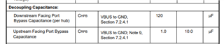
in our reference design, there's a 120uF for USB application. can this 120uF electrolytic capacitor be replaced by ceramic capacitor?
and can this 120uF be divided into several smaller capacitors?
Generally, it should be ok, but please pay attention to the following differences:
1. The value of ceramic capacitor can drop when the applied voltage is higher. Please choose ceramic capacitors with higher voltage rating or leave more margin in capacitance selection.
2. Ceramic caps usually have relatively smaller ESR. When several smaller caps in parallel the ESR can be even smaller. The dumping performance can be influences so please check whether it's necessary to add small resistors in the loop.
3. Thermal performance can be different, please check the application condition and datasheets.
4. The price can be different.
ou need to add the 120uF cap, you can refer to the below document.
M335x USB ID pin is controlled like follows.

USBn_ID has voltage applied by 120kΩ Pull Up. Does this circuit damage AM335x?
AM335x didn't change to USB Host even they pulled off the 120kΩ Pull Up.
Yes, this circuit will certainly damage the AM335x device. Please see bullet #1 in the schematic review checklist.
processors.wiki.ti.com/.../AM335x_Schematic_Checklist
another question is if we don't use the FAULT function, can this pin left float? I see it's an OD structure.
Yes, I think you can leave it float if you are not using it, since it's active-low open-drain output.
RE: How to get strong Noise immunity on AM335x VBUS line.
I have reviewed the internal design specification and the VBUS comparator circuits do not appear to have any hysteresis. However, this should not be required because the VBUS capacitance will filter the signal and remove all high frequency transients. I would like to know why you are asking this question since this question is not related to the original topic of protecting the input from over-voltage transients. Hysteresis doesn't protect inputs from over-voltage transients.
The internal PHY was designed to support OTG, so the VBUS terminal has an internal impedance of 40k - 100k ohms to ground as defined in the USB OTG specification.
PROCESSOR-SDK-AM335X: AM335X USB controller internal detection of VBUS logic
The VBUS detection follows the VBUS session definition in the USB2.0 Specification. The system design should follow the USB Spec.
Internally it is a set of analog comparators that detect the VBUS voltage window. I'm attaching the below image for reference only. It is from much newer device TRM (AM65x) and my sole intention is to depict the principles of VBUS detection.
Figure FOR REFERENCE ONLY!!! It is not from AM335X TRM!
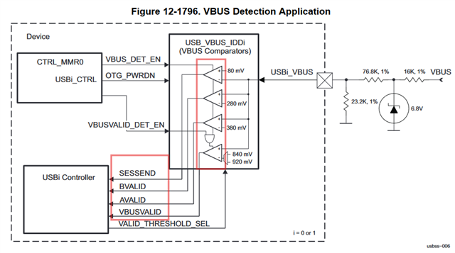
1) Are you trying to use true USB-OTG or USB DRD (Dual Role Device). The primary difference is that in DRD, dynamic role-reversal is not supported. In other words, if we enumerate as a Host/Device, we remain a Host/Device for the entirety of the session.
2) There are 2 controller VBUS state-machine checks prior to asserting USBn_VBUS:
https://e2e.ti.com/support/processors-group/processors/f/processors-forum/361790/am335x-usb-vbus
The primary function of this resistor is to limit current through D6 (Zener clamp diode) in case there is a transient voltage on VBUS that exceeds the absolute maximum input voltage of 5.25 volts. However, D6 was not installed on the starter kit so it is important your application does not cause VBUS to exceed 5.25 volts.
Please confirm the attached connection. Do we need an RC circuit in addition to this for VBUS line?
The USB specification defines the following capacitors on VBUS.
A standard USB host must have a minimum of 120uF on VBUS.
A USB peripheral must have less than 10uF on VBUS.
A Dual-role USB OTG device must have between 1uF and 6.5uF on VBUS.
This allows a USB peripheral to be hot plugged with a uncharged 10uf VBUS capacitor and the 120uF host capacitor provides enough charge sharing capacity to prevent VBUS from dropping below the specified voltage. You should perform the VBUS droop test as defined by USBIF test procedures to make sure the ferrite bead in this path does not cause you to fail this test.
The original USB specification did not define a minimum VBUS capacitance for a USB peripheral but I think they published a recommendation several years ago to use at least a 1uF capacitor on VBUS to prevent transient events on the peripheral VBUS signal when the cable is hot plugged/unplugged.
I have seen other customers use a ferrite bead on VBUS, but think this was done to minimize conducted emissions from coupling onto the VBUS cable and becoming radiated emissions.
Regards,
Sreenivasa
FYI, AM3352: Automotive qualification
The automotive variant of AM335x is DRA60x/DRA61x Jacinto5 Entry device. This is Automotive Qualified Device (AEC-100). This device datasheet is under NDA, and you should contact your local TI representative to get it. The TRM and silicon errata are common with AM335x device.
(+) AM335x built-in bandgap sensor - Processors forum - Processors - TI E2E support forums
I have checked with the factory team and they confirmed the answers I gave you above. Here is what they said:
"If a customer really needs thermal shutdown feature with AM335x, an external temperature sensor can be added on board for monitoring board temperature and estimating junction temperature. Linux thermal driver needs to be modified for using a thermal sensor used on the board."
Please refer to Application Report, SPRA953, for a description how the junction temperature can be determined.
http://www.ti.com/lit/an/spra953b/spra953b.pdf
The Thermal Resistance Characteristics for AM335x devices can be found in the data sheet.
http://www.ti.com/lit/gpn/am3358
Thank you for reply. But I have one additional question about method to estimate junction temperature.
* According to datasheet, there is following description about thermal resistance characteristics.
" Table5-12 provides simulation data and may not represent actual use-case values"
So, the question is, Q1. Can we use these parameter to estimate junction temperature on customer's system board ?
Measuring the temperature on top of the AM335x package and using these thermal resistance parameters to calculate the junction temperature will give better results than trying to use an ambient temp sensor to determine junction temperature.
Regards,
Sreenivasa
Hi Board Designers,
Inputs related to PDN - capacitors recommendations for Processor supply rails.
https://www.ti.com/lit/ds/symlink/am3358.pdf
Reference:
7444.TMDSSK3358_3H0009_REV1_3A_SCH.pdf
5.9 External Capacitors
To improve module performance, decoupling capacitors are required to suppress the switching noise generated by high frequency and to stabilize the supply voltage. A decoupling capacitor is most effective when it is close to the device, because this minimizes the inductance of the circuit board wiring and interconnects.


Reference:
2335.tmdxice3359_sch_3h0013_v2_1a.pdf

Schematic Reference
0763.TMDSSK3358_3H0009_REV1_3A_SCH.pdf
Regards,
Sreenivasa
Hi Board Designers,
Inputs related to PDN - Inputs related to DDR3 interface capacitors recommendations for processor and memory device
https://www.ti.com/lit/ds/symlink/am3358.pdf
7.7.2.3 DDR3 and DDR3L Routing Guidelines including capacitors
This section provides the timing specification for the DDR3 interface as a PCB design and manufacturing specification. The design rules constrain PCB trace length, PCB trace skew, signal integrity, cross-talk, and signal timing. These rules, when followed, result in a reliable DDR3 memory system without the need for a complex timing closure process. For more information regarding the guidelines for using this DDR3 specification, see Understanding TI's PCB Routing Rule-Based DDR Timing Specification. This application report provides generic guidelines and approach. All the specifications provided in the data manual take precedence over the generic guidelines and must be adhered to for a reliable DDR3 interface operation

Note section of data sheet DDR3 Signal Termination when VTT terminations are not used

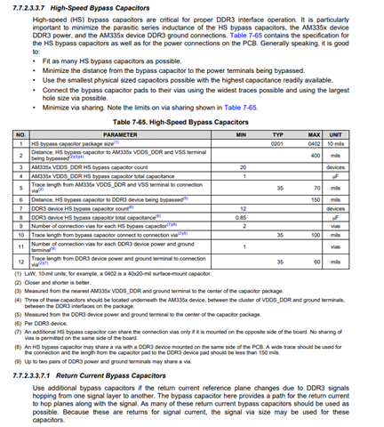


Schematics reference

Schematic reference:
5700.TMDSSK3358_3H0009_REV1_3A_SCH.pdf
Is DDR CLK_P/N termination required?
With proper trace impedance, we have never required that the differential clock be terminated for single device DDR3 designs with AM335x. Don’t forget, AM335x max DDR freq is 400MHz (vs 800MHz for AM64x), so I believe we started recommending this for AM64x and beyond due to the increased frequencies. I found some discussion of this here:
Let me try to explain why you may not need to terminate the differential clock as you suggest.
There is a very good chance you may not need to terminate the clock at the DDR3 end of the transmission line if you design your PCB clock traces to the recommended characteristic impedance defined in Table 5-58 of the AM335x Data Sheet.
The following description only applies in the case where you use a single DD3 device and all signal traces are connected point-to-point.
When a voltage transition in launched on the transmission line, the voltage of the signal trace at the source will suddenly transition to a voltage defined by the voltage divider equation [Vout = Vin * Z2 / (Z1+Z2)] where Z2 is the characteristic impedance of the transmission line, Z1 is the impedance of the AM335x output buffer, and Vin is VDDS_DDR. The voltage at the source end of the transmission line will remain at this voltage until the voltage transition propagates to the DDR3 high impedance input which causes the voltage transition to be reflected and returned to the source. Once the reflection returns to the source the voltage at the source will complete the transition to VDDS_DDR. If you monitor the voltage at source end of the transmission line with a scope, it appears to step up to a mid-supply voltage level for a short period of time before it continues to transition to VDDS_DDR. This short period of time where the voltage is mid-supply will be two times the signal trace propagation time.
This mid-supply voltage step can be seen anywhere along the transmission line, but the period of time where the voltage is mid-supply gets shorter as you approach the DDR3 end of the transmission line and completely goes away at he DDR3 end of the transmission line. If you monitor the voltage at the DDR3 end of the transmission line, you would not see this mid-supply voltage step since this is were the voltage transition encounters the impedance discontinuity that causes the refection. Therefore, the DDR3 device sees a clean low-to-high or high-to-low voltage transition.
If the characteristic impedance of the PCB signal trace matches the impedance of the AM335x output buffer the returned reflection does not see an impedance discontinuity so there is no additional reflections to cause signal integrity issues. When these impedances are matched the mid-supply voltage step should be [VDDS_DDR / 2].
This behaviour is the same for single ended or differential signals as long as the impedance of the PCB signal trace matches the impedance of the AM335x output buffer and the only other impedance discontinuity is the high-impedance input of the DDR3 device.
We still recommend system performance should verified by performing signal integrity analysis using specific PCB design details before implementing this topology.
From the AM335X Datasheet Rev. G, section 7.7.2.3.3.9:
"Figure 7-48 provides an example DDR3 schematic with a single 16-bit DDR3 memory device that does not have VTT termination on the address and control signals. A typical DDR3 point-to-point topology may provide acceptable signal integrity without VTT termination. System performance should be verified by performing signal integrity analysis using specific PCB design details before implementing this topology."
As an alternative you could directly copy the Beaglebone Black DDR3 layout (you should keep the same PCB stackup too). Beaglebone Black design files can be found here: http://elinux.org/Beagleboard:BeagleBoneBlack#Hardware_Files
Regards,
Sreenivasa
Hi Board Designers,
Inputs related to crystal ground connection


Regards,
Sreenivasa
Hi Board Designers,
Inputs related to connection of signals for RTC functionality
Schematic Checklist (reference in the above FAQ)
AM335x Schematic Checklist
www.ti.com/.../sprabn2
Previous revision that includes RTC information
2.14 RTC
Table 2 describes what to do with each pin related to RTC functionality. Three use case scenarios are
provided:
• RTC-only mode: If you will be using the low power RTC-only mode. This use case allows low power
operation of the AM335x by allowing only the RTC power supply to be ON while all the remaining
supplies are OFF.
• RTC timer functionality but no RTC-only mode: If you will be using the RTC feature but do not need
RTC-only mode. This use case allows you to use the Real Time clocking features (keeping time), but
you do not need to support the low power RTC-only mode.
www.ti.com References
SPRABN2–March 2019 9
Submit Documentation Feedback
Copyright © 2019, Texas Instruments Incorporated
AM335x schematic checklist
• RTC feature disabled: If you will never use the RTC features. In this use case, the RTC functions are
fully disabled.
sprabn2.pdf
2.14 RTC
Table 2 describes what to do with each pin related to RTC functionality. Three use case scenarios are provided:
• RTC-only mode: If you will be using the low power RTC-only mode. This use case allows low power operation of the AM335x by allowing only the RTC power supply to be ON while all the remaining supplies are OFF.
• RTC timer functionality but no RTC-only mode: If you will be using the RTC feature but do not need RTC-only mode. This use case allows you to use the Real Time clocking features (keeping time), but you do not need to support the low power RTC-only mode.

Regards,
Sreenivasa
Hi Board Designers,
Inputs related to cold and warm reset
https://www.ti.com/lit/ug/spruh73q/spruh73q.pdf
8.1.7 Reset Management
8.1.7.1 Overview
The PRCM manages the resets to all power domains inside device and generation of a single reset output
signal through device pin, WARMRSTn, for external use. The PRCM has no knowledge of or control over
resets generated locally within a module, e.g., via the OCP configuration register bit
IPName_SYSCONFIG.SoftReset.
All PRM reset outputs are asynchronously asserted. These outputs are active-low except for the PLL
resets. Deassertion is synchronous to the clock which runs a counter used to stall, or delay, reset deassertion upon source deactivation. This clock will be CLK_M_OSC used by all the reset managers. All
modules receiving a PRCM generated reset are expected to treat the reset as asynchronous and
implement local re-synchronization upon de-activation as needed.
One or more Reset Managers are required per power domain. Independent management of multiple reset
domains is required to meet the reset sequencing requirements of all modules in the power domain


Regards,
Sreenivasa
Hi Board Designers,
Inputs related to current measurement provision
Schematic Checklist (reference in the above FAQ)
AM335x Schematic Checklist
www.ti.com/.../sprabn2


Regards,
Sreenivasa
Hi Board Designers,
Inputs related to PRU GPIO
AM3358: What is the maximum achievable speed of dedicated PRU GPIO toggling
I have not observed any limitations in hardware testing. Based on the datasheet, your code should be fine as long as the pulse width for both input and output signals is at least 10ns (2 PRU clock cycles). Refer to the datasheet for more details.

Inputs related to enabling pulls for processor IOs
In case there is a discrepancy between the TRM and processor specific data sheet for the default pull configuration, the recommendation is to follow the data sheet:
(12) PULLUP OR PULLDOWN TYPE: Denotes the presence of an internal pullup or pulldown resistor. Pullup and pulldown resistors can be enabled or disabled via software


9.3.1.50 conf__ Register (offset = 800h–A34h)


Data sheet pin attributes
IOs that are driven low or high without enabling the internal pulls


IO that have pulldown enabled after reset

TRM pad control registers

(+) AM335x pad register offset info - Processors forum - Processors - TI E2E support forums
Regards,
Sreenivasa
Hi Board Designers,
Inputs related to Slew Control for IOs

The Pin multiplexing details for GPIO1[8] is given below.
Bit 6 : SLEWCTRL : Fast – 0
Bit 5: RXACTIVE : Receiver Enabled : 1 (Since GPIO1[8] shall be used an Input pin)
Bit 4: PULLTYPESEL : Pullup selected : 1
Bit 3: PULLUDEN : Pullup/pulldown enabled – 0
Bits 2:0 : MUXMODE : 7
Therefore the pin multiplexing code for GPIO1[8] is:
HWREG(SOC_CONTROL_REGS + CONTROL_CONF_UART_CTSN(0)) = (0x20 | 0x10| 0x7)
These are the basic steps to toggle the GPIO line
Pinmux:-
Do pinmux configurations accordingly
GPIO:- Set gpio3 pin to high
Set GPIO value:
gpio_reg_val = 0x00000008; /* for GPIO3 */
writel(gpio_reg_val, GPIO0_BASE + 0x194);
Set GPIO direction:
gpio_reg_val = readl(GPIO0_BASE + 0x134);
gpio_reg_val &= ~(0x00000008);
writel(gpio_reg_val, GPIO0_BASE + 0x134);
Note: Make sure that same pinmux registers are not configured for different purpose
(+) AM335X and GPIO1_20/GPIO3_18 - Processors forum - Processors - TI E2E support forums
What do you mean by address? If you need the address of the pinmux register for the pin you should check the AM335X TRM Rev. L section 9.3.1. Registers named conf_xxxxxxx are the pinmux registers. Pins are named after the pin function in mode 0.
Thus GPIO3_18 is on pin MCASP0_ACLKR (pinmux register conf_mcasp0_aclkr), resp. GPIO1_20 is on pin GPMC_A4 (pinmux register conf_gpmc_a4).
(+) GPIO INPUT FLOATING DEFAULT VALUE - Processors forum - Processors - TI E2E support forums
The slew rate control changes the output buffer drive strength during the rise/fall transitions. I suspect the slew rate is changing at the AM335x terminal or you would not see a difference in SPI1 operation. You may need to measure the slew rate with a high speed oscilloscope and high speed FET probe as close as possible to the AM335x terminal to see the difference. If you make this measurement at the far end on the PCB signal trace using low bandwidth equipment, the high frequency portion of the signal transition will be filtered and may not be possible to see the difference.
I think your problem may be related to a signal integrity issue on the AM335x end of the SPI clock.
The SPI clock is driven out of the SPI1_SCLK terminal to the external device and is also looped back into the AM335x device via the internal IO buffer. Therefore, any signal integrity issue on the SPI1_SCLK terminal end of the PCB signal trace can corrupt the clock signal.
Using the SPI1_SCLK terminal as an input and output simultaneously creates a signal integrity issue at the SPI1_SCLK terminal. The source impedance of the output buffer and transmission line impedance of the circuit board etch creates a voltage divider at the SPI1_SCLK terminal during rising and falling edges of the SPI clock. The voltage at the SPI1_SCLK terminal will change by [VDD * (ZL/(ZL + RS))] when the output buffer toggles and will remain at that voltage until it propagates to the load and the reflection returns. During this time the amplitude of the SPI1_SCLK terminal is close to the switching threshold of the input buffer. Noise may cause the input buffer to generate glitches or invalid transitions of the SPI clock. This will cause problems for the internal SPI logic.
The figure below is provided to help visualize the circuit topology that creates a voltage divider and resultant voltage waveform.

This problem can be resolved by placing a series termination resistor between the SPI1_SCLK terminal and the transmission line. This increases the amplitude of the SPI1_SCLK terminal voltage divider step above the switching threshold so noise will not generate any glitches. This resistor should always be placed as close as possible to the SPI1_SCLK terminal that is sourcing the SPI clock. The value recommended for this resistor is between 22 and 50 ohms. As the resistor value increases the amplitude of the voltage divider step will increase. However the maximum SPI clock speed will decrease. The actual value may need to be determined after the circuit board is fabricated.
Do you have a series termination resistor installed on the AM335x end of the SPI clock?
You right.. We added a resistor between the SPI1_SCLK terminal and the transmission line. It now works.
(+) AM3352: Slow Slew Rate - Processors forum - Processors - TI E2E support forums
1. No, it's available, however the AM335x datasheet has the following statement: 'The timing parameter values specified in this data manual assume the SLEWCTRL bit in each pad control register is configured for fast mode (0b).' This statement applies to all peripherals.
2. No, it will not be ignored, but you will not see any significant difference, as explained in the thread you refer.
(+) AM335x Slow Slew Rate - Processors forum - Processors - TI E2E support forums
Slew rate control is a function implemented in the IO cell of the device and does not have any relationship to specific peripherals. So slew rate control is applied on a per terminal basis via the respective conf_<module>_<pin>_slewctrl bit, where '<module>_<pin>' is the terminal name.
We also determined the IO cells used in AM335x were not providing any significant change in slew rate. Therefore, there wasn't any value in characterizing the device while operating in slow mode.
We do not recommend using slow mode and there is no data for slow mode because of the reasons mentioned above.
I have seen other customers add filters which I assume were inserted to reduce radiated emission.
The LCD should be one of the easier peripherals to filter since all signals are propagating from AM335x to the display. If you use the same filter design on each signal, the insertion delay through the filter should be very similar which allows all signals to retain their timing relationship. However, you may cause signal integrity issues if you slow down the edges too much relative to the fastest signal toggle rate required by the LCD interface.
This is a system level issue which has multiple dependencies that should be considered to determine the best solution for your product.
(+) AM3352: I/O Slew Rates - Processors forum - Processors - TI E2E support forums
The answers to their questions have been answered in the post you referenced.
Does TI have published specifications for the output slew rate of the TX and RX outputs of the UARTs on the AM3352?
We do not publish the output slew, only the max loading (Timing Conditions).
I'm referring https://e2e.ti.com/support/processors/f/791/p/233997/1121323#1121323.
1) Does this mean that the SLOW setting is not available on all pins?
2) If I set SLOW slew rate for it then the setting is ignored? (The setting is forced to FAST?)
1. No, it's available, however the AM335x datasheet has the following statement: 'The timing parameter values specified in this data manual assume the SLEWCTRL bit in each pad control register is configured for fast mode (0b).' This statement applies to all peripherals.
2. No, it will not be ignored, but you will not see any significant difference, as explained in the thread you refer.
If you search the AM335x Data Sheet (SPRS717) for the word "SLEWCTRL", you would find the following statement in the Peripheral Information and Timings section.
The timing parameter values specified in this data manual assume the SLEWCTRL bit in each pad control register is configured for fast mode (0b).
All AM335x Data Sheet timing parameters are based on SLEWCTRL being configured in fast mode. Therefore, slow mode is not support on any of the peripheral interfaces.
The SPIx_SCLK is internally looped back at the pin (as shown in the image peaves posted in the original thread) and used by AM335x to sample the RX data. Any signal integrity issue on the SPIx_SCLK pin will impact the input clock, which is why a series termination resistor is needed.
The SLEWCTRL bits affect the slewrate of the signal. Please note that we only characterized fast mode. While your customer's problem seems to be solved by the SLEWCTRL bits, they could be on the edge and changing SLEWCTRL to slow mode may not be a robust solution across PTV Process - Temperature - Voltage.
(+) GPIO INPUT FLOATING DEFAULT VALUE - Processors forum - Processors - TI E2E support forums
(+) AM335x and DDR3 termination - Processors forum - Processors - TI E2E support forums
All peripheral timing closure was done based on the I/O configured for fast slew. Slow mode is not supported on any peripheral interface and that is why we do not publish timing information for operating in slow mode.
I do not have access to ROM code, so cannot answer your other question. I will forward this post to someone that may be able to answer this question.
(+) AM335x LCD_DATA slew rate and EMI - Processors forum - Processors - TI E2E support forums
If you search the AM335x Data Sheet (SPRS717) for the word "SLEWCTRL", you would find the following statement in the Peripheral Information and Timings section.
The timing parameter values specified in this data manual assume the SLEWCTRL bit in each pad control register is configured for fast mode (0b).
All AM335x Data Sheet timing parameters are based on SLEWCTRL being configured in fast mode. Therefore, slow mode is not support on any of the peripheral interfaces.
The setup, hold, and output delay timing requirements for each peripheral signal is defined before the processor design is completed. The design team will modify the internal circuit delays in the processor to make sure the timing parameters are as good or better than the pre-defined values. When they performed this task, known as timing closure, they assumed all IO slew rates were configured in fast mode. Which means we cannot guarantee the signals meet the values defined in the data sheet if slow mode is selected.
The errata is used to document unexpected behaviors that were not accounted for in initial documentation. We knew from day one, slow mode was not supported and the data sheet has always defined this at the beginning of the Peripheral Information and Timings chapter. Therefore, no plans to put this in the errata.
Please refer to the second paragraph of Section 5.1.1 in the data sheet. It states "The timing parameter values specified in this data manual assume the SLEWCTRL bit in each pad control register is configured for fast mode (0b)."
AM335x peripheral interfaces were only characterized with SLEWCTRL configured for fast slew rate, so all interfaces should be configured for fast slew rate.
Regards,
Sreenivasa
Hi Board Designers,
Inputs related to processor clocking, crystal grounding
During reset, on some of the units the display flickers. If customer changes the crystal to oscillator, the issue is resolved. Customer is pushing for a root cause.
There is a errata for the crystal grounding.
Is it Ok for customer to use the crystal following the errata or is the recommendation to use an oscillator as clock source.
The customer is ultimately responsible for design a robust system. They need to use a solution that is robust in their system design. A solution that works for one customer may not work for another.
Many customers are able to use the crystal circuit with the updated ground connection without any issue. However, some customers have a very noisy system design that allows noise to couple into the crystal circuit and the coupling of noise into the crystal circuit generates glitches on the internal reference clock. Glitches on the reference clock can effectively over-clock internal state-machines, which cause unexpected behavior.
The reference clock signal generated by the crystal circuit has a slow rise/fall times relative to the rise/fall time provided by an LVCMOS oscillator. The slow rise/fall signal from the crystal circuit has a higher susceptibility to noise creating non-monotonic events on the signal transition as it passed though the switching threshold of the input buffer. It is difficult for noise to produce non-monotonic events on the transition of the faster rise/fall signal generated by an LVCMOS oscillator.
The customer has two choices. The first choice is, determine the noise source / coupling mechanism into the crystal circuit and eliminate the noise or coupling. The second choice is, use the less noise susceptible LVCMOS clock source solution.
Most PCB designers know all of the crystal circuit components should be placed very close together and near the oscillator terminals. When the PCB is designed this way, the crystal component ground connections would be very close together, so we expected each ground connection to be a direct connection to the digital ground plane (VSS). It is not necessary to connect them together with single point connection to ground.
I will define the crystal component grounds to clarify this point. There should be three or four crystal component grounds.
1. The first ground connection is for C1
2. The second ground connection is for C2
3. The third ground connection is for the respective oscillator ground (VSS_OSC or VSS-RTC).
4. This fourth ground is an optional connection to ground for the crystal package shield if the crystal selected has a shield.
AM335x - Advisory 1.0.30: OSC0/OSC1 noise immunity
You mentioned the customer ‘tied the crystal to ground’. I need to understand what this comment means.
Does this mean they only tied the crystal package/case to ground or did they tie the VSS_OSC/VSS_RTC terminal and all crystal component grounds to the nearest PCB digital ground?
Advisory 1.0.30 recommends the VSS_OSC/VSS_RTC terminal and all crystal circuit grounds should be connected to the nearest PCB ground.
I have never seen a case where this recommendation has caused more noise to couple into the crystal circuit.
We were not able to measure the noise because adding a probe to the crystal circuit influences noise coupling. We reached our conclusion based on two weeks of testing multiple PCB designs with various noise sources.
We do not make any specific recommendations related to crystal package, but all the boards we tested were using small 4 terminal ceramic SMT crystals and two of the terminals were also connected to the nearest PCB digital ground.
A 1.8 v digital clock source can be used to replace the crystal circuit and it will be much more difficult to couple noise into this clock source. The digital clock source has fast rise/fall edges that transition through the input switching threshold very quickly and is not as susceptible to noise while the crystal circuit produces a near sine-wave signal that slowly transition through the input switching threshold.
e2e.ti.com/.../am3358-am335x-osc0-crystal-circuit-load-capacitance
e2e.ti.com/.../system-time-jump-problem-and-am335x-advisory-1-0-30
The oscillator input buffer has a switching threshold voltage where the output will change states as the voltage applied to the input crosses the threshold. The voltage applied to the oscillator input buffer is a slow changing sinusoidal signal when using a crystal circuit as the reference clock. Noise coupled to this slow slew rate signal may cause the output of the oscillator input buffer to toggle several times as the signal slowly crosses the switching threshold. If this occurs, the internal clock signal will think these unexpected toggles are real clock toggles. However, these unexpected toggles are much higher in frequency than the real clock toggles. These much faster toggles will violate internal circuit timing and in some cases may cause the circuits to perform unexpected operations. For example, portions of the RTC counter circuit may see these fast toggles and respond properly while other portions of the RTC counter circuit do not see the fast toggles. In such a case, the RTC counter may not function as expected and do very unpredictable things like counting backward.
If this happens, any internal circuits being clocked from the oscillator output may perform unexpected operations. In most cases the DPLLs acts like a filter and circuits being clock from the DPLLs never see these unexpected toggles. We saw one case of a DPPL performing an unexpected operation while debugging this issue, but as mention above any circuit being clocked from the oscillator could perform unexpected operations when excess noise is coupled to the oscillator input signal.
This issue is completely eliminated if you use a fast slew rate clock source like you get from an LVCMOS clock source. It is also much harder to cause this issue on the Master oscillator vs the RTC oscillator because the slew rate of the 19.2 MHz - 26 MHz oscillator is much faster than the 32.768 KHz oscillator.
e2e.ti.com/.../am335x-power-rails-gnd-connections
e2e.ti.com/.../vss_osc-and-vss_rtc-connection-to-pcb-ground
The VSS_OSC terminal has a higher impedance connection to the internal ground of OSC0 that the VSS terminal, so the decoupling capacitor is not as effective as it could be if it were connected VSS rather than VSS_OSC.
The TI EVM has the same mistake and we have not had any reports of this causing a problem. However, the EVM is normally used in a lab and may not be exposed to the same environmental conditions (like temperature variations, external electrical noise, and etc) as a production product.
Based on my experience, I would be much more concerned with the issue described in Advisory 1.0.30.
e2e.ti.com/.../1025821
e2e.ti.com/.../am335x-what-are-the-implications-of-connecting-vss_osc-to-vss-in-a-system-that-uses-an-external-crystal
AM335x - Advisory 1.0.30: OSC0/OSC1 noise immunity
A 1.8 v digital clock source can be used to replace the crystal circuit and it will be much more difficult to couple noise into this clock source. The digital clock source has fast rise/fall edges that transition through the input switching threshold very quickly and is not as susceptible to noise while the crystal circuit produces a near sine-wave signal that slowly transition through the input switching threshold.
High frequency digital switching current flowing through inductive substrate traces and bond wires that connect the silicon die to the PCB ground produces a few milivolts of ground noise on the die relative to the PCB ground.
When the crystal circuit is referenced to the PCB ground and the oscillator input is referenced to the die ground, the oscillator input will see this high frequency ground noise summed with the crystal output voltage. This can potentially increase clock jitter since the crystal output voltage is a relative slow changing sinusoidal signal and the high frequency ground noise can cause the oscillator input to see slightly shorter or longer clock cycles.
The Kelvin ground allows the crystal circuit ground to be at the same potential as the die ground and reduces the oscillator input noise.
There should not be any change in power supply consumption.
e2e.ti.com/.../732530
The LVCMOS digital clock source connected to the OSC0 XTALIN terminal should be powered by the same source as connected to VDDS_OSC terminal.
The LVCMOS digital clock source connected to the OSC1 RTC_XTALIN terminal should be powered by the same source as connected to VDDS_RTC terminal.
Both VDDS_OSC and VDDS_RTC terminals have a recommended nominal operating voltage of 1.8 volts.
The OSC0 VSS_OSC terminal and OSC1 VSS_RTC terminal should be connected to the digital ground when using external LVCMOS clock sources.
e2e.ti.com/.../583015
As I now understand it on the ZCZ package, both the main oscillator, OSC0, and the external RTC oscillator, OSC1, have floating Kelvin ground terminals, VSS_OSC and VSS_RTC respectively. Can you please recommend how to wire VSS_RTC when OSC1 is not being used.
Each Kelvin ground terminal should be only connected to the respective external crystal components as shown in the OSC0 Crystal Circuit Schematic data manual figure when a crystal is connected to the respective oscillator.
Each Kelvin ground terminal should be connected to the PCB ground when an LVCMOS digital clock source is connected to the respective oscillator.
When not using the RTC oscillator (OSC1) the VSS_RTC Kelvin ground terminal should be connected to the PCB ground.
e2e.ti.com/.../the-connection-of-oscillator-on-tmdssk3358
If the oscillator package has ground terminals, those terminals should also be connected to the respective Kelvin ground terminals (VSS_RTC or VSS_OSC).
The decoupling capacitor connected to the VDDS_OSC (R11) terminal should not be connected to the GND_OSC0 net which is connected to the VSS_OSC (V11) terminal as shown in the schematic. This capacitor should have been connected to VSS.
Regards,
Sreenivasa