This thread has been locked.
If you have a related question, please click the "Ask a related question" button in the top right corner. The newly created question will be automatically linked to this question.
Tool/software: TI C/C++ Compiler
Hello, ti experts,
My SDK version is PSDK-07_01_00_11.
Are there write protection restrictions on the operation of the CTRLMMR_PCIE_REFCLK1_CLKSEL register?
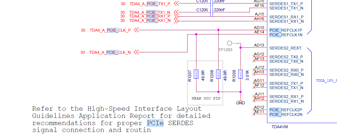
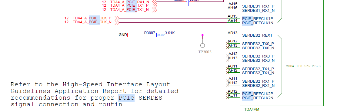
I am currently debugging PCIe's function of using internal clock output, using PCIe1.
Refer to the following post
I need to modify the following registers
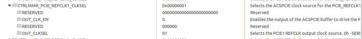
1. CTRLMMR_PCIE_REFCLK1_CLKSEL, bit8 is set to 1, and bit1~0 is set to 1;
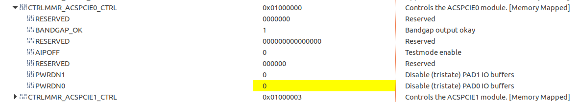
2.CTRLMMR_ACSPCIE1_CTRL; bit1 and bit0 are both set to 0
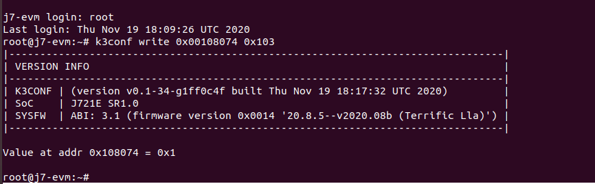
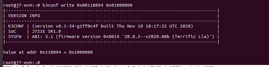
I tried three methods to modify the value of the register, CTRLMMR_PCIE_REFCLK1_CLKSEL can not be modified, always keep the default value 0x01; CTRLMMR_ACSPCIE1_CTRL can be modified;
1. After starting the linux system, modify it through the k3conf write 0x00108074 0x103 instruction;
2. Use the ccs debug method to load vxlinux symbol on a72, and directly modify the register through ccs after startup.
3. Modify the linux device tree and driver code to achieve the modification;
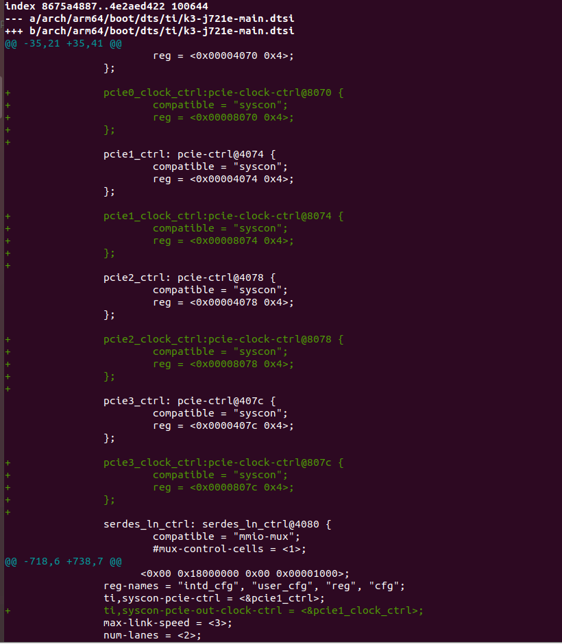
Add syscon option in dts file:
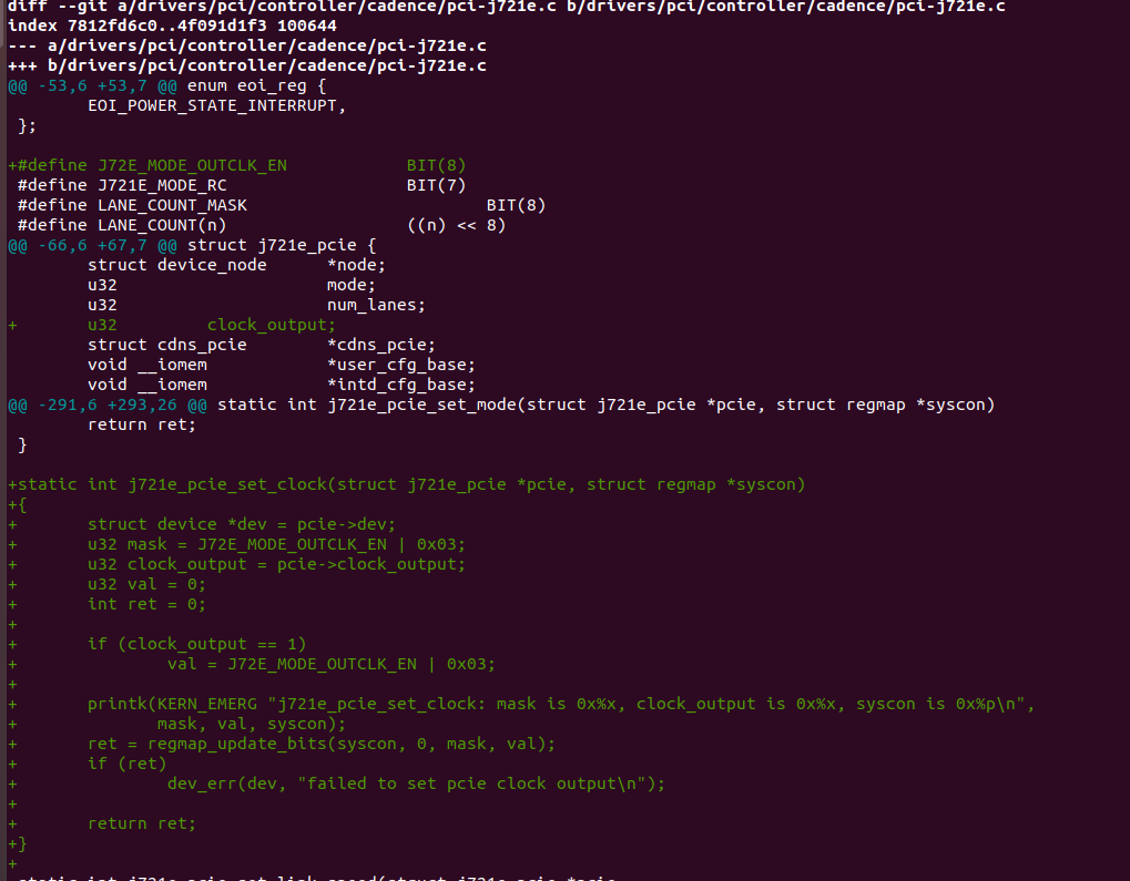
Make the following changes in the driver/pci/controller/cadence/pci_j72e.c file:
Then, start linux, use the same method as method 1 to read the register, the result is the same as method 1
Hi Kepei,
Where did you probe for the clocks in the EVM? As for the configurations, there are only CTRLMMR_PCIE_REFCLK1_CLKSEL and CTRLMMR_ACSPCIE1_CTRL to be configured.
Thanks
Kishon
Hi Kishon,
Thanks for your reply!
What does "Where did you probe for the clocks in the EVM?" mean?
I configured the register CTRLMMR_PCIE_REFCLK1_CLKSEL to 0x101 and CTRLMMR_ACSPCIE1_CTRL to 0x01000000 through the k3config write command after linux started, but there is no clock output.
Thanks!
Kepei
Hi Kepei,
I'm trying to understand how you are saying there is no clock output? Where did you probe the clock signals?
Thanks
Kishon
Hi Kishon,
I used an oscilloscope to measure the output signal of the oscilloscope, and the ground and probe of the oscilloscope respectively measured the 2 pins of the differential signal PCIE_REFCLK1P and PCIE_REFCLK1N.
Thanks
Kepei
Hi Kepei,
Did you also made the necessary board modifications to route to the connector? Since you have mentioned TDA4VM in the subject, I think it's the same EVM provided by TI?
Thanks
Kishon
Hi Kishon,
The following is the schematic diagram. TDA4VM_A provides the clock to TDA4VM_B, the clock signal I tested on the pull-down resistor of the clock pin.
The circuit principle is the same as EVM, except that EVM is a PCI clock provided by an external clock, so there is no solder pull-down resistor.
Thanks
Kepei
Hi Kishon,
Okay, thank you very much and look forward to your answer.
Regards
Kepei
Hi Kepei,
We haven't yet been able to do the board modification. Meanwhile after reviewing, I have the following patch. Please use the attached patch (in addition to control module register modification) and check if you see any clocks?
Thanks
Kishon
From d83bdd855d02d34ec8e5dc5258e250c9be355004 Mon Sep 17 00:00:00 2001 From: Kishon Vijay Abraham I <kishon@ti.com> Date: Wed, 6 Jan 2021 14:11:47 +0530 Subject: [PATCH] route_external_fix Signed-off-by: Kishon Vijay Abraham I <kishon@ti.com> --- drivers/phy/cadence/phy-cadence-sierra.c | 58 ++++++++++++++++++++++++ 1 file changed, 58 insertions(+) diff --git a/drivers/phy/cadence/phy-cadence-sierra.c b/drivers/phy/cadence/phy-cadence-sierra.c index 309aa30f1c03..96452e5ee8bc 100644 --- a/drivers/phy/cadence/phy-cadence-sierra.c +++ b/drivers/phy/cadence/phy-cadence-sierra.c @@ -28,6 +28,7 @@ #define SIERRA_CMN_PLLLC_LF_COEFF_MODE1_PREG 0x49 #define SIERRA_CMN_PLLLC_LF_COEFF_MODE0_PREG 0x4A #define SIERRA_CMN_PLLLC_LOCK_CNTSTART_PREG 0x4B +#define SIERRA_CMN_PLLLC_CLK1_PREG 0x4D #define SIERRA_CMN_PLLLC_BWCAL_MODE1_PREG 0x4F #define SIERRA_CMN_PLLLC_BWCAL_MODE0_PREG 0x50 #define SIERRA_CMN_PLLLC_SS_TIME_STEPSIZE_MODE_PREG 0x62 @@ -144,12 +145,22 @@ #define SIERRA_MAX_LANES 16 #define PLL_LOCK_TIME 100000 +#define SIERRA_PHY_PMA_COMMON_OFFSET(block_offset) \ + (0xE000 << (block_offset)) +#define PHY_PMA_CMN_CTRL1 0x0000U + static const struct reg_field macro_id_type = REG_FIELD(SIERRA_MACRO_ID_REG, 0, 15); static const struct reg_field phy_pll_cfg_1 = REG_FIELD(SIERRA_PHY_PLL_CFG, 1, 1); static const struct reg_field pllctrl_lock = REG_FIELD(SIERRA_PLLCTRL_STATUS_PREG, 0, 0); +static const struct reg_field phy_pma_cmn_ctrl_rcv_out_en = + REG_FIELD(PHY_PMA_CMN_CTRL1, 6, 7); +static const struct reg_field cmn_plllc_clk1outdiv = + REG_FIELD(SIERRA_CMN_PLLLC_CLK1_PREG, 0, 6); +static const struct reg_field cmn_plllc_clk1_en = + REG_FIELD(SIERRA_CMN_PLLLC_CLK1_PREG, 12, 12); struct cdns_sierra_inst { struct phy *phy; @@ -193,10 +204,14 @@ struct cdns_sierra_phy { struct reset_control *apb_rst; struct regmap *regmap_lane_cdb[SIERRA_MAX_LANES]; struct regmap *regmap_phy_config_ctrl; + struct regmap *regmap_phy_pma_common_cdb; struct regmap *regmap_common_cdb; struct regmap_field *macro_id_type; struct regmap_field *phy_pll_cfg_1; + struct regmap_field *phy_pma_cmn_ctrl_rcv_out_en; struct regmap_field *pllctrl_lock[SIERRA_MAX_LANES]; + struct regmap_field *cmn_plllc_clk1outdiv; + struct regmap_field *cmn_plllc_clk1_en; struct clk *clk; struct clk *cmn_refclk_dig_div; struct clk *cmn_refclk1_dig_div; @@ -268,6 +283,14 @@ static struct regmap_config cdns_sierra_phy_config_ctrl_config = { .reg_read = cdns_regmap_read, }; +static struct regmap_config cdns_sierra_phy_pma_cmn_config = { + .name = "sierra_phy_pma_cmn", + .reg_stride = 1, + .fast_io = true, + .reg_write = cdns_regmap_write, + .reg_read = cdns_regmap_read, +}; + static int cdns_sierra_phy_init(struct phy *gphy) { struct cdns_sierra_inst *ins = phy_get_drvdata(gphy); @@ -417,6 +440,20 @@ static int cdns_regfield_init(struct cdns_sierra_phy *sp) } sp->macro_id_type = field; + field = devm_regmap_field_alloc(dev, regmap, cmn_plllc_clk1outdiv); + if (IS_ERR(field)) { + dev_err(dev, "cmn_plllc_clk1outdiv reg field init failed\n"); + return PTR_ERR(field); + } + sp->cmn_plllc_clk1outdiv = field; + + field = devm_regmap_field_alloc(dev, regmap, cmn_plllc_clk1_en); + if (IS_ERR(field)) { + dev_err(dev, "cmn_plllc_clk1_en field init failed\n"); + return PTR_ERR(field); + } + sp->cmn_plllc_clk1_en = field; + regmap = sp->regmap_phy_config_ctrl; field = devm_regmap_field_alloc(dev, regmap, phy_pll_cfg_1); if (IS_ERR(field)) { @@ -425,6 +462,14 @@ static int cdns_regfield_init(struct cdns_sierra_phy *sp) } sp->phy_pll_cfg_1 = field; + regmap = sp->regmap_phy_pma_common_cdb; + field = devm_regmap_field_alloc(dev, regmap, phy_pma_cmn_ctrl_rcv_out_en); + if (IS_ERR(field)) { + dev_err(dev, "phy_pma_cmn_ctrl_rcv_out_en field init failed\n"); + return PTR_ERR(field); + } + sp->phy_pma_cmn_ctrl_rcv_out_en = field; + for (i = 0; i < SIERRA_MAX_LANES; i++) { regmap = sp->regmap_lane_cdb[i]; field = devm_regmap_field_alloc(dev, regmap, pllctrl_lock); @@ -478,6 +523,15 @@ static int cdns_regmap_init_blocks(struct cdns_sierra_phy *sp, } sp->regmap_phy_config_ctrl = regmap; + block_offset = SIERRA_PHY_PMA_COMMON_OFFSET(block_offset_shift); + regmap = cdns_regmap_init(dev, base, block_offset, reg_offset_shift, + &cdns_sierra_phy_pma_cmn_config); + if (IS_ERR(regmap)) { + dev_err(dev, "Failed to init PHY PMA common CDB regmap\n"); + return PTR_ERR(regmap); + } + sp->regmap_phy_pma_common_cdb = regmap; + return 0; } @@ -651,6 +705,10 @@ static int cdns_sierra_phy_probe(struct platform_device *pdev) if (!sp->autoconf && sp->nsubnodes > 1 && !already_configured) regmap_field_write(sp->phy_pll_cfg_1, 0x1); + regmap_field_write(sp->phy_pma_cmn_ctrl_rcv_out_en, 0x3); + regmap_field_write(sp->cmn_plllc_clk1_en, 0x1); + regmap_field_write(sp->cmn_plllc_clk1outdiv, 0x2e); + pm_runtime_enable(dev); phy_provider = devm_of_phy_provider_register(dev, of_phy_simple_xlate); return PTR_ERR_OR_ZERO(phy_provider); -- 2.17.1
Hi Kishon
Thank you so much for your prompt reply!
Is this patch file based on psdk-7.1?
Thanks
Kepei
Hi Kishon,
I tested it according to your suggestion;
1. Added the patch you provided;
2. Recompile the kernel;
3. Replace the Image file;
4. Start linux;
5. The k3conf write command unlocks the register;
6.k3conf write 0x00108074 0x101 command to modify the CTRLMMR_PCIE_REFCLK1_CLKSEL register
7.k3conf write 0x00118094 0x01000000 modify the CTRLMMR_ACSPCIE1_CTRL register
But unfortunately, there is still no clock output on the pin.
If possible, can you test it on the EVM board?
Thanks
Kepei
Kepei,
We are working on this and we should have an update in the next few days.
Regards
Karthik
Hi Karthik,
Alright, thank you very much!
Looking forward to your results.
Thanks
Kepei
Kepei,
Can you confirm if you rescaned the PCIe bus after enabling clock?
I received my modified EVM and did a quick try with the patch, I was not able detect the SSD on the M2 slot. But one suspect is that the RC PLL shall be locked before he can gave out clock. could you try the same sequence on your side:
M.2 slot ====================================
//enable PADs of ACSPCIe
devmem2 0x00118094 w 0x01000000
//unlock CTRLMMR_LOCK2 for 8000h to 9FFFh
devmem2 0x00109008 w 0x68EF3490
devmem2 0x0010900C w 0xD172BC5A
//refclk select for ACSPCIe
devmem2 0x00108078 w 0x00000100
echo 1 > /sys/bus/pci/devices/0002:00:00.0/remove
echo 1 > /sys/bus/pci/rescan
I will sync up with Kishon and we may need to add these two registers in the patch to get the correct sequence.
regards
Jian
Hi Jian,
I'm very sorry, because some other work caused the delay. I just tested your suggestion, but there is still no clock output.
j7-evm login: root Last login: Thu Nov 19 18:09:28 UTC 2020 root@j7-evm:~# devmem2 0x00118094 w 0x01000000 /dev/mem opened. Memory mapped at address 0xffff95cd0000. Read at address 0x00118094 (0xffff95cd8094): 0x01000003 Write at address 0x00118094 (0xffff95cd8094): 0x01000000, readback 0x01000000 root@j7-evm:~# devmem2 0x00109008 w 0x68EF3490 /dev/mem opened. Memory mapped at address 0xffff95fb0000. Read at address 0x00109008 (0xffff95fb9008): 0x00000000 Write at address 0x00109008 (0xffff95fb9008): 0x68EF3490, readback 0x68EF3490 root@j7-evm:~# devmem2 0x0010900C w 0xD172BC5A /dev/mem opened. Memory mapped at address 0xffffb90a0000. Read at address 0x0010900C (0xffffb90a900c): 0x00000000 Write at address 0x0010900C (0xffffb90a900c): 0xD172BC5A, readback 0xD172BC5A root@j7-evm:~# devmem2 0x00108078 w 0x00000100 /dev/mem opened. Memory mapped at address 0xffffb6670000. Read at address 0x00108078 (0xffffb6678078): 0x00000000 Write at address 0x00108078 (0xffffb6678078): 0x00000100, readback 0x00000100 root@j7-evm:~# echo 1 > /sys/bus/pci/devices/0000\:00\:00.0/remove [ 639.633076] pci_generic_config_write32: 20 callbacks suppressed [ 639.633084] pci_bus 0000:00: 2-byte config write to 0000:00:00.0 offset 0x84 may corrupt adjacent RW1C bits [ 639.648797] pci_bus 0000:00: 2-byte config write to 0000:00:00.0 offset 0xdc may corrupt adjacent RW1C bits [ 639.658617] pci_bus 0000:00: 2-byte config write to 0000:00:00.0 offset 0xc8 may corrupt adjacent RW1C bits [ 639.668432] pci_bus 0000:00: 2-byte config write to 0000:00:00.0 offset 0x92 may corrupt adjacent RW1C bits [ 639.678155] pci_bus 0000:00: 2-byte config write to 0000:00:00.0 offset 0x9c may corrupt adjacent RW1C bits [ 639.687972] pci_bus 0000:00: 2-byte config write to 0000:00:00.0 offset 0x92 may corrupt adjacent RW1C bits [ 639.697723] pci_bus 0000:00: 2-byte config write to 0000:00:00.0 offset 0x4 may corrupt adjacent RW1C bits [ 639.707427] pci_bus 0000:00: 2-byte config write to 0000:00:00.0 offset 0x4 may corrupt adjacent RW1C bits [ 639.717112] pci_bus 0000:01: busn_res: [bus 01] is released root@j7-evm:~# echo 1 > /sys/bus/pci/rescan [ 654.149076] pci 0000:00:00.0: [104c:b00d] type 01 class 0x060400 [ 654.155149] pci_bus 0000:00: 2-byte config write to 0000:00:00.0 offset 0x4 may corrupt adjacent RW1C bits [ 654.164813] pci_bus 0000:00: 2-byte config write to 0000:00:00.0 offset 0x4 may corrupt adjacent RW1C bits [ 654.174486] pci_bus 0000:00: 2-byte config write to 0000:00:00.0 offset 0x92 may corrupt adjacent RW1C bits [ 654.184216] pci_bus 0000:00: 2-byte config write to 0000:00:00.0 offset 0xb2 may corrupt adjacent RW1C bits [ 654.193969] pci 0000:00:00.0: supports D1 [ 654.197968] pci 0000:00:00.0: PME# supported from D0 D1 D3hot [ 654.203707] pci_bus 0000:00: 2-byte config write to 0000:00:00.0 offset 0x84 may corrupt adjacent RW1C bits [ 654.215396] pci_bus 0000:00: 2-byte config write to 0000:00:00.0 offset 0x3e may corrupt adjacent RW1C bits [ 654.227230] pci_bus 0000:00: 2-byte config write to 0000:00:00.0 offset 0x3e may corrupt adjacent RW1C bits [ 654.236995] pci_bus 0000:00: 2-byte config write to 0000:00:00.0 offset 0x3e may corrupt adjacent RW1C bits [ 654.246730] pci_bus 0000:00: 2-byte config write to 0000:00:00.0 offset 0x3e may corrupt adjacent RW1C bits [ 654.256470] pci 0000:00:00.0: PCI bridge to [bus 01] [ 654.261430] pci_bus 0000:00: 2-byte config write to 0000:00:00.0 offset 0x1c may corrupt adjacent RW1C bits [ 654.271449] pcieport 0000:00:00.0: PME: Signaling with IRQ 36 [ 654.277723] pcieport 0000:00:00.0: AER: enabled with IRQ 36
Thank you very much for your help!
Kepei
Hi,
Update my test status:
I set another TDA4_B to ep mode, and enter the following command after TDA4_B linux startup:
mount -t configfs none /sys/kernel/config cd /sys/kernel/config/pci_ep/ mkdir functions/pci_epf_test/func1 echo 0x104c > functions/pci_epf_test/func1/vendorid echo 0xb00d > functions/pci_epf_test/func1/deviceid echo 2 > functions/pci_epf_test/func1/msi_interrupts echo 2 > functions/pci_epf_test/func1/msix_interrupts ln -s functions/pci_epf_test/func1 controllers/2910000.pcie-ep/ echo 1 > controllers/2910000.pcie-ep/start
Then set TDA4_A to rc mode, and look for the patch provided by Kishon in the kernel source code. During the startup of TDA4_A, I can see that rc scans ep, but then the kernel dumps and the output log is as follows.
[ 1.434116] j721e-pcie 2910000.pcie: Link up [ 1.438486] j721e-pcie 2910000.pcie: host bridge /bus@100000/pcie@2910000 ranges: [ 1.446147] j721e-pcie 2910000.pcie: IO 0x18001000..0x18010fff -> 0x18001000 [ 1.453624] j721e-pcie 2910000.pcie: MEM 0x18011000..0x1fffffff -> 0x18011000 [ 1.461174] j721e-pcie 2910000.pcie: PCI host bridge to bus 0000:00 [ 1.467581] pci_bus 0000:00: root bus resource [bus 00-0f] [ 1.473185] pci_bus 0000:00: root bus resource [io 0x0000-0xffff] (bus address [0x18001000-0x18010fff]) [ 1.482875] pci_bus 0000:00: root bus resource [mem 0x18011000-0x1fffffff] [ 1.489916] pci 0000:00:00.0: [104c:b00d] type 01 class 0x060400 [ 1.496065] pci_bus 0000:00: 2-byte config write to 0000:00:00.0 offset 0x4 may corrupt adjacent RW1C bits [ 1.505934] pci_bus 0000:00: 2-byte config write to 0000:00:00.0 offset 0x4 may corrupt adjacent RW1C bits [ 1.515821] pci_bus 0000:00: 2-byte config write to 0000:00:00.0 offset 0xe8 may corrupt adjacent RW1C bits [ 1.525779] pci_bus 0000:00: 2-byte config write to 0000:00:00.0 offset 0x3e may corrupt adjacent RW1C bits [ 1.535745] pci_bus 0000:00: 2-byte config write to 0000:00:00.0 offset 0x92 may corrupt adjacent RW1C bits [ 1.545707] pci_bus 0000:00: 2-byte config write to 0000:00:00.0 offset 0xb2 may corrupt adjacent RW1C bits [ 1.555692] pci 0000:00:00.0: supports D1 [ 1.559785] pci 0000:00:00.0: PME# supported from D0 D1 D3hot [ 1.565656] pci_bus 0000:00: 2-byte config write to 0000:00:00.0 offset 0x84 may corrupt adjacent RW1C bits [ 1.577397] pci 0000:00:00.0: bridge configuration invalid ([bus 00-00]), reconfiguring [ 1.585578] pci_bus 0000:00: 2-byte config write to 0000:00:00.0 offset 0x3e may corrupt adjacent RW1C bits [ 1.595537] pci_bus 0000:00: 2-byte config write to 0000:00:00.0 offset 0x3e may corrupt adjacent RW1C bits [ 1.605495] pci_bus 0000:00: 2-byte config write to 0000:00:00.0 offset 0x3e may corrupt adjacent RW1C bits [ 1.615518] pci 0000:01:00.0: [104c:b00d] type 00 class 0xff0000 [ 1.621724] pci 0000:01:00.0: reg 0x10: [mem 0x00000000-0x000000ff] [ 1.628138] pci 0000:01:00.0: reg 0x14: [mem 0x00000000-0x000001ff] [ 1.634551] pci 0000:01:00.0: reg 0x18: [mem 0x00000000-0x000003ff] [ 1.640964] pci 0000:01:00.0: reg 0x1c: [mem 0x00000000-0x00003fff] [ 1.647381] pci 0000:01:00.0: reg 0x20: [mem 0x00000000-0x0001ffff] [ 1.653794] pci 0000:01:00.0: reg 0x24: [mem 0x00000000-0x000fffff] [ 1.660437] pci 0000:01:00.0: supports D1 [ 1.664530] pci 0000:01:00.0: PME# supported from D0 D1 D3hot [ 1.670469] pci 0000:01:00.0: reg 0x224: [mem 0x00000000-0x003fffff 64bit] [ 1.677495] pci 0000:01:00.0: VF(n) BAR0 space: [mem 0x00000000-0x00ffffff 64bit] (contains BAR0 for 4 VFs) ERROR: Unhandled External Abort received on 0x80000000 from S-EL1 ERROR: exception reason=0 syndrome=0xbf000000 Unhandled Exception from EL1 x0 = 0xffff800014670000 x1 = 0x0000000000000000 x2 = 0x000000000080000a x3 = 0x0000000000000003 x4 = 0xffff800014900000 x5 = 0xffff80001050e820 x6 = 0xffff8000117ef8f4 x7 = 0x000000000000ea60 x8 = 0x0000000080b5111d x9 = 0x00000000b00d104c x10 = 0x7f7f7f7f7f7f7f7f x11 = 0x0101010101010101 x12 = 0xffff0008400fe227 x13 = 0xffff0008400fe91c x14 = 0xffffffffffffffff x15 = 0xffff000840372f28 x16 = 0xffff800014410000 x17 = 0x0000000000000001 x18 = 0x0000000000000000 x19 = 0xffff8000117ef834 x20 = 0x0000000000000004 x21 = 0x0000000000000000 x22 = 0x0000000000000004 x23 = 0xffff8000117ef834 x24 = 0x0000000000000001 x25 = 0xffff8000110ee210 x26 = 0x0000000000000001 x27 = 0x0000000000000000 x28 = 0xffff000841e56800 x29 = 0xffff8000117ef780 x30 = 0xffff8000104dd930 scr_el3 = 0x000000000000073d sctlr_el3 = 0x0000000030cd183f cptr_el3 = 0x0000000000000000 tcr_el3 = 0x0000000080803520 daif = 0x00000000000002c0 mair_el3 = 0x00000000004404ff spsr_el3 = 0x0000000020000085 elr_el3 = 0xffff8000104dd948 ttbr0_el3 = 0x0000000070010b00 esr_el3 = 0x00000000bf000000 far_el3 = 0x0000000000000000 spsr_el1 = 0x0000000060000005 elr_el1 = 0xffff800010115b44 spsr_abt = 0x0000000000000000 spsr_und = 0x0000000000000000 spsr_irq = 0x0000000000000000 spsr_fiq = 0x0000000000000000 sctlr_el1 = 0x0000000034d4d91d actlr_el1 = 0x0000000000000000 cpacr_el1 = 0x0000000000300000 csselr_el1 = 0x0000000000000000 sp_el1 = 0xffff8000117ef780 esr_el1 = 0x0000000000000000 ttbr0_el1 = 0x0000000083090000 ttbr1_el1 = 0x0000000082df0000 mair_el1 = 0x0000bbff440c0400 amair_el1 = 0x0000000000000000 tcr_el1 = 0x00000034f5507510 tpidr_el1 = 0xffff80086ebe0000 tpidr_el0 = 0x0000000000000000 tpidrro_el0 = 0x0000000000000000 par_el1 = 0x0000000000000000 mpidr_el1 = 0x0000000080000000 afsr0_el1 = 0x0000000000000000 afsr1_el1 = 0x0000000000000000 contextidr_el1 = 0x0000000000000000 vbar_el1 = 0xffff800010081800 cntp_ctl_el0 = 0x0000000000000005 cntp_cval_el0 = 0x00000021b4b50b31 cntv_ctl_el0 = 0x0000000000000000 cntv_cval_el0 = 0x0000000000000000 cntkctl_el1 = 0x00000000000000e6 sp_el0 = 0x000000007000a3d0 isr_el1 = 0x0000000000000040 dacr32_el2 = 0x0000000000000000 ifsr32_el2 = 0x0000000000000000 cpuectlr_el1 = 0x0000001b00000040 cpumerrsr_el1 = 0x0000000000000000 l2merrsr_el1 = 0x0000000000000000
According to this phenomenon, I think whether the ep side is detected by the rc side, but what error on the ep side causes the rc side kernel to start wrong?
At the same time, I still did not test the clock signal on the clock pin.
Regards
Kepei
Hi
Update my test status again.
The previous kernel dump status may be caused by overheating of the chip.
After cooling the chip again, I started TDA4_A as the RC side, and executed the operation provided by Jian.
At present, I can read and write the ep device on the TDA4_B side normally. Thank you very much for your help.
My next question is, can I implement these manual operations in the Linux driver or device tree?
Regards
Kepei