Hi Team,
Q1:
I am wondering about the blue part and red part description in datasheet chapter 7.5.2 as below screenshot.
I think the two descriptions are inconsistent even conflicting, or it is just my misunderstanding.
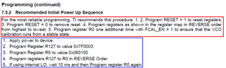
Is the right power sequence as below steps?
- Power On Device.
- Reset = 1, R0<D1> to reset register.
- Reset = 0, R0<D1> to remove reset.
- Program Register R127 to value 0x7F0003.
- Program Register R6 to value 0x 060100
- Program Register R127 to R0 in reverse order
- If using internal LO, wait 10msec.
- Program Register R0 <D3> for FCAL_EN = 1 to ensure that the VCO calibration runs from a stable state.
Q2:
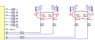
For the IF output from LMX8410L, could TI team advise the value of series capacitor to ADC devices?
The IF frequency will be zero frequency, or close to zero frequency.
Will the 0.01uF be right for Zero-IF architecture?
Thanks.